RECIF Technologies Presents R.PACK Software Suite: The next step in efficiency and control
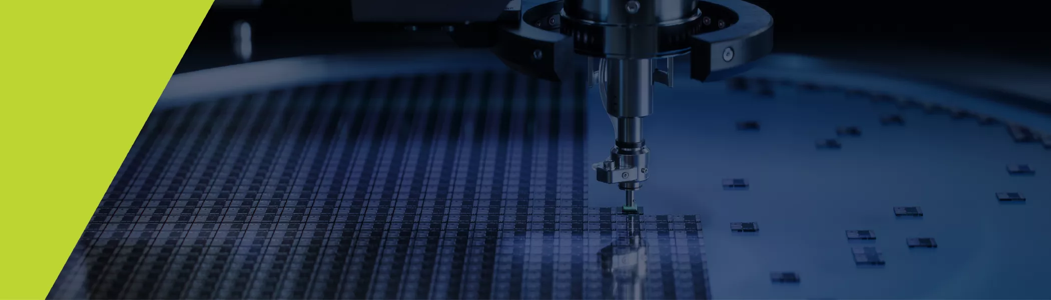
Toulouse, 5 June 2025 – RECIF Technologies is pleased to announce the launch of R.PACK, the next-generation software suite designed for RECIF sorters. With an emphasis on usability, efficiency, and innovation, R.PACK introduces a suite of advanced features aimed at simplifying the management of wafer sorting equipment.
Built for Speed, Designed for Precision
R.PACK enhances operational efficiency for users of RECIF’s COMPACT and SMART sorters, featuring advanced capabilities and a modern interface designed to streamline wafer sorting processes
Key Features of R.PACK:
Refined User Interface: The design of R.PACK makes it easier than ever to create recipes and monitor jobs, ensuring smoother operations and increased productivity.
Seamless Transition: Current users will experience minimal disruption when transitioning to R.PACK, thanks to its intuitive interface that simplifies adoption.
Ongoing Software Enhancements: R.PACK is built on a forward-compatible framework, with updates released annually to deliver new features and performance improvements. The first major update was rolled out in January 2025, with the next release scheduled for Q1 2026 — part of an ongoing roadmap to enhance user experience and expand system capabilities.
Commitment to Innovation and User Experience
The release of R.PACK reinforces RECIF Technologies’ ongoing commitment to providing high-performance solutions for the semiconductor industry. By focusing on a more intuitive and efficient wafer sorting process, R.PACK marks the first in a series of improvements designed to elevate both the user experience and operational efficiency.
"We believe R.PACK will significantly enhance our customers' workflows and performance," said Thomas Brillouet, the R&D Manager at RECIF Technologies. "By providing enhanced features and a modernized interface, we empower our customers with tools that maximize safety, enhance efficiency, and optimize equipment performance with minimal effort."
Availability and Future Updates
The first major update for R.PACK is available now, with additional updates scheduled annually every Q1. R.PACK is compatible with RECIF sorters (COMPACT & SMART) and will fully replace the WISE software by 2027.
For more information on R.PACK, including system requirements and update schedules, visit www.reciftech.com.
In this engaging two-hour Masterclass organized by SEMI, we explore the groundbreaking role of magnetic materials, particularly magnetic nanoparticles (MNPs), in biomedical fields. The session commences with an in-depth review of the physics and synthesis of MNPs, including comprehensive discussions on fundamental theories, synthesis methods, and advanced MNP surface functionalization strategies. Attendees will gain insights into the characterization techniques used to analyze the physicochemical properties of MNPs.
The Masterclass transitions to the applications of MNPs in therapeutic and diagnostic contexts. We will review cutting-edge MNP-based therapies, such as magnetic hyperthermia therapy, targeted drug and gene delivery, and magnetic neurostimulation. In addition, we will discuss various MNP-based diagnostic techniques, including magnetoresistive (MR) sensing, nuclear magnetic resonance (NMR), magnetic particle spectroscopy (MPS), magnetic resonance imaging (MRI), and magnetic particle imaging (MPI). A critical focus of this Masterclass will be on safety and biocompatibility issues associated with the use of MNPs in vivo, examining the toxicity of MNPs, immune responses, and their circulation time in the human body.
The latter part of the session will introduce participants to the innovative field of micromagnetic neural stimulation, an infant yet extremely promising field. We will delve into the design and efficacy of micromagnetic devices, such as the Magnetic Pen (MagPen) and Magnetic Patch (MagPatch) Array, which utilize micrometer-sized coils (μcoils) for targeted neural activation. This is particularly for patients with spinal cord injuries (SCI) and for reducing opioid dependency, with insights drawn from current research supported by the NIH Blueprint Medtech Program. By the end of the Masterclass, attendees will have a comprehensive understanding of the potential clinical applications of MNPs and MEMs-based micromagnetic neurostimulators.
ABOUT THE SPEAKER
Dr. Renata Saha, Senior Scientist, Dupont
Dr. Renata Saha is a Senior Scientist at DuPont located in Wilmington, DE. She holds a PhD in Electrical and Computer Engineering from the University of Minnesota, Twin Cities, which she earned in August 2023. Her undergraduate degree in Electronics & Communication Engineering was obtained from the National Institute of Technology in Durgapur, India. During the summer of 2017, she was an undergraduate research intern at Conseil européen pour la Recherche Nucléaire (CERN), located in Geneva, Switzerland working on the ALICE experiment upgrade.
Dr. Saha is the recipient of 3-year College of Science & Engineering Fellowship, Women in Technology Scholarship 2021-2022 from Cadence Design Systems, and the Graduate Neuromodulation Research Fellowship 2022-2023 from MnDRIVE. She was also elected an iREDEFINE Fellow in 2022 by ECEDHA and was named a Rising Star in EECS. She has published over 30 journal articles, 3 US patents, and 2 book chapters.
Her expertise and research interests involve designing and developing microelectromechanical systems (MEMs) devices for neuromodulation and cardiovascular monitoring, characterizing magnetic nanoparticles (MNPs) for potential biomarkers. Outside of her research and work, Dr. Saha is trained in Indian classical dance form, Odissi, and enjoys performing and choreographing the art form.
In this two-hour Masterclass, Dupont Senior Scientist Renata Saha delves into the biomedical applications of magnetic nanoparticles (MNPs), covering their manufacturing, functionalization as well as therapeutic and diagnostic uses including safety considerations such as biocompatability and toxicology.
Innovations in Magnetic Materials: Application in Biomedical Engineering
Flexible Electronics Master Class #26
10:00 am - 12:00 pm
Off
Add to Calendar2025-10-29 10:00:002025-10-29 12:00:00FEMC #26 Innovations in Magnetic Materials: Applications in Biomedical EngineeringIn this two-hour Masterclass, Dupont Senior Scientist Renata Saha delves into the biomedical applications of magnetic nanoparticles (MNPs), covering their manufacturing, functionalization as well as therapeutic and diagnostic uses including safety considerations such as biocompatability and toxicology. United StatesSEMI.org[email protected]America/Los_Angelespublic
America/Los_Angeles
Watch Now!
The first part of the course provides a brief overview of semiconductor design and fabrication steps, encompassing IC design techniques, all wafer processing steps, assembly, and packaging. It delves into semiconductor jargon in laypeople terms, and various substrate types such as Si, SiGe, FDSOI, GaAs, SiC, GaN. Additionally, it discusses different types of transistors like pMOS, nMOS, Bipolar, BiCMOS, CMOS, FinFets, and GAA and their evolution and what applications they are used in.
The second part of the course focuses on semiconductor business aspects such as silicon economics, wafer processing costs, semiconductor revenue forecasts, driving forces in the industry, top semiconductor IDMs, market competitors based on market share, OEMs, foundries, top tool vendors, and Fabless companies. Addresses the fastest-growing semiconductor markets based on geographic locations and applications, identifies semiconductor competitors/customers, and discusses major semiconductor markets like Automotive, PC, Mobile, Memory, Wireless, Cell phones, Consumer, Gaming, AI, IoT, Digital TV, Radio, Automotive, MEMS, and Emerging Technology & Impact on Industry.
Learning Objectives
Understand the fundamental principles and theories semiconductor technology.
Communicate with other associates and understand wafer processing steps.
Understand semiconductor business aspects such as silicon economics, wafer processing costs, semiconductor revenue forecasts, driving forces in the industry, top semiconductor IDMs, market competitors based on market share, OEMs, foundries, top tool vendors, and Fabless companies.
Review the semiconductor eco-system as it relates to design and fabrication of a semiconductor device.
Gain knowledge of major semiconductor markets like Automotive, PC, Mobile, Memory, Wireless, Cell phones, Consumer, Gaming, AI, IoT, Automotive, MEMS, and Emerging Technology & Impact on Industry.
Demonstrate effective communication skills through written reports, presentations, and discussions related to semiconductor subjects.
Collaborate effectively with peers in group projects or discussions regarding semiconductor subjects.
Analyze and evaluate research literature in semiconductor technology.
Develop critical thinking and problem-solving skills applicable to semiconductor technology.
Who Should Attend
This course is suitable for anyone seeking a better understanding of the semiconductor industry, market leaders, terminology, business, and the semiconductor ecosystem.
See what course participants had to say about this course!
"Denny Frye knows so much about the history of the semiconductor industry that he was able to tie together many different industries and technologies that I have heard about but never knew how they were connected."
"Great overview of the semiconductor industry & market."
"This was a very detailed course on many facets of the industry, would recommend!"
"It was a great mix of technical and overview of the key players in the market!"
"Good blend on technical and commercial topics."
"Excellent introduction to the semiconductor world."
"Great session on the understanding of the semiconductor industry in a nutshell."
Important Information
Note that only the person who registered will receive a certificate of completion. This virtual training will not be recorded. Attendees must be present to access course knowledge.
Can't find the training link day of? After you register, you will receive the link to the live training via the email address you provided. In addition, you will receive email reminders about 24 hours in an advance and an hour before with the same link. Please keep these emails on hand to access the trainings on time. If you do not see any confirmation emails, please check your junk/spam folders before contacting SEMI U for support.
Embark on a journey through semiconductor design, manufacturing, and business in this illuminating course. Explore IC design techniques, transistor evolution, and market dynamics. Delve into substrate types and industry economics, discovering the fastest-growing markets and key players shaping the semiconductor landscape.
Pricing
Early Bird Special - $100 off until May 12th.
Members:$845 $745
Non-Members: $945 $845
* Group pricing for 20 attendees: $9900 Any questions, please contact [email protected]
Understanding Semiconductor Technology and Business
Virtual Training - Europe
8:00 am - 4:30 pm
Off
Add to Calendar2026-05-26 08:00:002026-05-26 16:30:00Understanding Semiconductor Technology and Business (Europe) Embark on a journey through semiconductor design, manufacturing, and business in this illuminating course. Explore IC design techniques, transistor evolution, and market dynamics. Delve into substrate types and industry economics, discovering the fastest-growing markets and key players shaping the semiconductor landscape.PricingEarly Bird Special - $100 off until May 12th. Members: $845 $745Non-Members: $945 $845* Group pricing for 20 attendees: $9900Any questions, please contact [email protected]GermanySEMI.org[email protected]Europe/Brusselspublic
Europe/Brussels
Register Now
Leverage SEMI U learning offerings to wrap up your 2025 professional development journey! Our pledge remains unwavering: providing comprehensive, technical education to equip you with the skills needed for a prosperous journey in the semiconductor sector.
Are you ready to take your semiconductor industry knowledge to the next level? We're thrilled to invite you to our upcoming webinar titled "SEMI University - 2025 and beyond." This webinar promises to be an informative session where you'll gain insights into the latest updates, exciting live trainings at SEMICON West and virtually the remainder of this year and beyond.
During this webinar, you can expect to:
Discover the latest updates and enhancements to SEMI U's course catalog.
Learn about the exciting live, in-person training courses scheduled for SEMICON West.
Review upcoming virtual instructor-led trainings.
Gain access to a special 10% discount on ALL on-demand courses.
Join us to discover our current course offerings, upcoming in-person and virtual trainings, and more. Engage in a Q&A session. Plus, by attending this free webinar, you'll receive a 10% discount code for all on-demand courses and will be entered into a raffle to win a FREE course bundle ($100 value).
8:00 am - 8:30 am
Off
Add to Calendar2025-09-25 08:00:002025-09-25 08:30:00SEMI University - 2025 & BeyondJoin us to discover our current course offerings, upcoming in-person and virtual trainings, and more. Engage in a Q&A session. Plus, by attending this free webinar, you'll receive a 10% discount code for all on-demand courses and will be entered into a raffle to win a FREE course bundle ($100 value). Choose your session:US/EU: 8:00 AM – 8:30 AM PT [Register Now]Asia/US: 5:00 PM – 5:30 PM PT [Register Now]United StatesSEMI.org[email protected]America/Los_AngelespublicRegister Now
TRI and Bosch Partner on AI Solution for MEMS Packaging
Test Research, Inc. (TWSE: 3030), the leading test and inspection systems provider for the electronics manufacturing industry, is proud to announce its successful partnership with Bosch in the development of an AI visual check solution for MEMS packaging.
Bosch has recognized TRI's valuable contribution to their success in MEMS packaging in 2025 with a Certificate of Appreciation. The certificate acknowledges the successful completion of the AI visual check for MEMS packaging, highlighting the strong cooperation and partnership between the two companies.
This collaboration demonstrates TRI's expertise in AI-driven inspection solutions and its commitment to providing valuable solutions for the electronics manufacturing industry. TRI's AI-powered solutions include the AI Defect Detection, AI Smart Programming, AI Verify Host, AI training tool, AI Station, and more.
TRI (TWSE: 3030), offers the most robust product portfolio in the industry for Automatic Test and Inspection solutions. Learn more at http://www.tri.com.tw. For sales and service information, please write to us at [email protected] or call +886-2-2832 8918.
Stanton Chase Welcomes Sundar Rajan Ramalingam as Partner in the Semiconductor Practice
Stanton Chase is pleased to announce that Sundar Rajan Ramalingam has joined the firm as a Partner in North America. His addition strengthens the firm's executive search and leadership consulting capabilities for the semiconductor sector at a time of rapid transformation.
Sundar brings nearly three decades of leadership experience across manufacturing and global technology sectors. He has scaled a multi-billion-dollar global engineering division and supported the growth of several Global Capability Centers (GCCs). Within the semiconductor ecosystem, he has played a pivotal role in building and advising leadership teams across chip design, chip-to-cloud platforms, semiconductor fabs, and foundry operations.
This deep operational and strategic background gives Sundar a unique perspective on the evolving talent needs of semiconductor organizations.
"The semiconductor industry is entering a pivotal era—what I call a 'perfect leadership storm'—driven by generative AI, strategic autonomy imperatives, and breakthroughs like 3nm and advanced packaging," said Sundar. "While these trends are accelerating innovation, the industry also faces a growing talent gap. Companies need capable leaders who can navigate complexity, scale innovation, and build resilient teams. I plan to use my experience in technology and manufacturing to help semiconductor companies find executives who deliver results and foster sustainable growth."
Sundar's career spans both strategic HR leadership and general management with P&L responsibility, offering clients a rare blend of technical insight and leadership development expertise.
"Sundar fits well with our North American team and fills a specific need in our practice," said Mickey Matthews, Managing Director at Stanton Chase in North America and Chair of the Governance Committee. "His time working across borders gives him a genuine understanding of how global teams function. Blending this multicultural understanding with Sundar's deep technology products and services vertical expertise matters a lot to the clients we serve and specifically in the semiconductor space."
Jan-Bart Smits, Managing Partner at Stanton Chase Amsterdam and Global Sector Leader for Semiconductors, added: "Sundar joins us when the semiconductor industry sits at a turning point. Firms in this sector are looking for something different in their executives—people who understand both market forces and engineering details. Sundar knows this world and will further enhance our ability to serve chip makers and their suppliers."
As the semiconductor industry moves into a new chapter—marked by AI-driven demand, geopolitical shifts, and the race toward next-gen nodes—Sundar's appointment signals Stanton Chase's commitment to helping clients lead with confidence and clarity.
Sundar holds an MBA from XLRI Jamshedpur (India) and completed executive education programs, including the Chief Human Resource Officer Program at Wharton, University of Pennsylvania.
He will serve clients from Stanton Chase offices in Baltimore and Raleigh, USA, as well as Bangalore, Hyderabad, and Chennai, India—locations near semiconductor business centers.
Stanton Chase ranks among the top global retained executive search firms with more than 76 offices in 45 countries and a worldwide team of senior consultants. Stanton Chase serves clients across multiple industry specialties and places C-suite executives, senior managers, and board members for companies ranging from global corporations to emerging businesses. Stanton Chase belongs to the Association of Executive Search and Leadership Consultants (AESC), adhering to the highest industry standards of professionalism and ethics.
Join the Leaders of the Semiconductor Climate Consortium Scope 3 Working Group, plus other industry experts, to review the recently released Scope 3 Category 11 GHG Assessment and Guidance for the Semiconductor Value Chain. Compiled with the expert assistance of ERM, with input from all levels of the ecosystem, this document has been designed to align on reporting Scope 3, Category 11, an important step in measuring the impact of reduction efforts across the industry.
Review of the NEW SCC Scope 3.11 Emissions Calculation Guidance
A Webinar for the Semiconductor Ecosystem
8:00 am - 9:00 am
Off
Add to Calendar2025-06-12 08:00:002025-06-12 09:00:00Webinar - Category 3.11 ReviewJoin the Leaders of the Semiconductor Climate Consortium Scope 3 Working Group, plus other industry experts, to review the recently released Scope 3 Category 11 GHG Assessment and Guidance for the Semiconductor Value Chain. Compiled with the expert assistance of ERM, with input from all levels of the ecosystem, this document has been designed to align on reporting Scope 3, Category 11, an important step in measuring the impact of reduction efforts across the industry.Download the Guidance DocumentUnited StatesSEMI.org[email protected]America/Los_Angelespublic
America/Los_Angeles
All sessions are free of charge to Semiconductor Climate Consortium (SCC) and Energy Collaborative (EC) members. Others will be admitted by invitation on a case-by-case basis. Multiple attendees (up to 3) from your company are welcome, but must be invited. Exceptions can be made to the 3 persons limit to have the RIGHT people, with direct responsibility for subjects being discussed.
A gathering of the semiconductor value chain in one place to most efficiently share solutions and tools and workshop solutions, thereby optimizing your time and resources dedicated to addressing the specific challenges we face. The GCS Workshops are co-hosted by SEMI, the Semiconductor Climate Consortium, Apple, and Google.
The Workshops are focused on revealing the right details and data that will support action on decarbonization recommendations. The Workshops will NOT focus solely on the issue and roadblocks, but rather the solutions, including (1) sharing examples of successful paths, (2) provide possible tools you need to help address the gaps, and (3) active workshopping on further solution spacing towards emission reductions. We have identified leaders with the experience and knowledge to move toward answers during each Workshop.
Bring your experience, critical thinking skills, and share with your fellow sustainability travelers.
Workshop Themes and Layout
5/15 – Opening + Facilities Abatement Tours (Tours are now full)
5/20 (AM) - Data & Reporting Alignment – ROI and roadblocks + Closing (PM)
Synergies with the Semiconductor Climate Consortium
Many themes of the GCS Workshops are outcomes of the discoveries in the SCC Working Groups and previous Supplier Day presentations. The GCS Workshops will allow for greater depth of discussions and face-to-face solutioning opportunities. With the right information and the right audience, attendees will depart with tools to operationalize for action. Across the ecosystem, we want to see those benefits show up in our Scope 3 calculations.
Microsoft Offices & Sands Convention Center Singapore Singapore
12:00 pm
-
1:00 pm
Registration & Networking Lunch
Meet and connect with key industry stakeholders, policy leaders, and Microsoft’s sustainability leadership.
1:00 pm
-
1:10 pm
Mousumi Bhat, PhD
VP SEMI Sustainability
SEMI
SEMI Global Climate Summit Workshops: Welcome
1:10 pm
-
1:25 pm
Giorgio Fortunato
Google
Energy in the APAC Region: Outlook & Strategies
1:30 pm
-
1:45 am
Susannah Calvin
Environment & Supply Chain Innovation
Apple, Inc.
Journey to Carbon Neutral - Supply Chain Focus
1:45 pm
-
2:05 pm
Leslie Esparza
Director, Responsible Sourcing
Microsoft
Leo Aspauza
Microsoft
Moderator
Will Hudson
Microsoft
Reflections on Microsoft Supplier Days & Looking Forward
2:05 pm
-
2:15 pm
Mousumi Bhat, PhD
VP, Global Sustainability
SEMI
Overview of GCSW Workshops
2:15 pm
-
6:30 pm
Facilities Abatement Tours
(Tours are full and no longer available to new registrants.)
Workshop 1: Manufacturing Fab Scope 1 Emissions
8:30 am
-
8:50 am
Breakfast and Networking
8:50 am
-
9:20 am
Beth Elroy
Vice President, Global EHS & Sustainability
Micron
Collaborative solutions for emissions challenges
9:20 am
-
9:35 am
Cristal Phwan
APAC Sustainability Team Manager
GlobalFoundries
Fabs Deploying new abatement tech; brownfield retrofits
9:35 am
-
9:50 am
Robin Sim
Facility Manager - Operation & Hookup Program
STMicroelectronics
Innovative ways to complete brownfield retrofits while minimizing fab disruption
9:50 am
-
10:05 am
Dr. Hak Joon Kim
Principal Researcher
Korea Institute of Machinery and Materials (KIMM)
New abatement tech for both greenfield & brownfield fabs
10:05 am
-
10:20 am
Dr. Haein Cho
Samsung
Samsung's journey to net zero & Scope 1 strategies
Workshop 2: Manufacturing Energy Efficiency – fab/subfab interoperability, toolkits and ROI calculations
1:30 pm
-
2:00 pm
Kevin Chan
Lead, Artificial Intelligence
Micron
IDM perspective, state of the art sensor deployment & best practices for energy efficiency
2:00 pm
-
2:15 pm
James Oh
Aveva
Immediate Opportunities around Energy Efficiency
2:15 pm
-
2:30 pm
John Golightly
VP of Sustainability
ASM
ASM Energy Efficiency Story
Net Zero Operations through Innovation and Collaboration
2:30 pm
-
3:00 pm
EE Workshop 1: Sensor Deployment for Equipment
From energy sensor to harmonics & power quality detection and remediation
3:00 pm
-
3:45 pm
Shaun Crawford
Product Manager
Applied Materials
Stefanie Hammer
General Manager
Algorismic
Michael Neel
Director of Marketing
Inficon
Operations Energy Efficiency Opportunities, Process and Recommendations
State-of-the-art Sub-Fab Interoperability
3:45 pm
-
4:15 pm
TBD
EE Workshop 2: Communication & Interoperability
4:15 pm
-
4:45 pm
Slava Libman
FTD Solutions
James Oh
Aveva
Mark da Silva
SEMI Smart Manufacturing
Current Solutions - Data Aggregation & Dashboard: Case Study
4:45 pm
-
5:15 pm
Teh Tiack Ein
Head of Presales, Southeast Asia
Siemens Digital Industries Software
Arul Ambikapathi
Lam Research
Mark da Silva
SEMI Smart Data AI Initiative
Future Solution - Digital Twin (Design, Build, Operate & Maintain a Fab)
5:15 pm
-
5:45 pm
Workshop 3: Data Management & Reporting
5:45 pm
-
6:00 pm
Read out
Workshop 3: Renewable Energy Education & Advocacy – global state-of-play, market breakouts for education and solution short listing
8:00 am
-
8:30 am
Networking & Breakfast
8:30 am
-
9:00 am
Xin Wei Low
Assistant Chief Executive
EMA
The Net Zero Imperative and Singapore's Role
9:00 am
-
9:20 am
Will Hudson
Asia Pacific Sustainability Policy Director
Microsoft
One Goal, One Grid; Unlocking Clean Power Together
9:20 am
-
9:50 am
Ali Izadi-Najafabadi
Head of APAC
Bloomberg NEF
Global state of play on accessible RE
9:50 am
-
10:10 am
Mike Thomas
Managing Director
Lantau Group
Friendly Policies to Renewable Energy
10:10 am
-
10:20 am
Eric Gibbs
Clean Energy Buyers Association
Procurement Hub
10:30 am
-
12:00 pm
Breakouts/Workshop: RE Education & Awareness
Two parallel sessions will be held.
Group A - Room 3111: South Korea (45 min) and Japan (45 min)
Group B - Room 3112: Singapore/Malaysia (45 min) and Taiwan (45 min)
10:30 am
-
11:15 pm
Seiya Miyake
Renewable Energy Promoting Organization, Inc.
Shawn Woo
3 Degrees
How to Procure: Japan
11:15 am
-
12:00 pm
Ousam Jin
CREF
How to Procure: South Korea
10:30 am
-
11:15 am
Henry Eu
Asia Clean Energy Consortium (ACEC)
Gregory Thomassin
Business Development
Total Energies
Mike Thomas
LTG
How to Procure: Singapore/Malaysia
11:15 am
-
12:00 pm
Jung Choi
Regional Manager for Asia-Pacific
CRS
Wei-In Lin
Apala
How to Procure: Taiwan
12:00 pm
-
12:15 pm
Workshop Readout
12:30 pm
-
1:00 pm
Albert Sutanto
Manager SE Asia Markets and Global EACs Sourcin
Mt. Stonegate
Achieving 100% RE in Asia: Market Highlights and Corporate Sourcing
(a working lunch)
1:00 pm
-
1:20 pm
Robbert Slooten
Manager, Renewable Energy and Carbon Advisory
Schneider Electric
Bess Ng
Associate Principle, Sustainability Business
Schneider Electric
How to leverage the power of buyers’ groups for renewable electricity adoption in key markets - Korea, Singapore, and Japan
• Are these the right problems?
• What are 3 solutions that you can commit to working on this year?
• Where do you need help from the consortium or customers?
• What can we collectively commit to for 2030?
Workshop 5: Data & Reporting Alignment – ROI and roadblocks
8:30 am
-
9:00 am
Joe Palaazo
Technical PM - Environmental Sustainability
Google
Big Picture & Objective
9:00 am
-
9:30 am
Claus Cremers
Director Automotive Ecosystems, Siemens, AG
Member of the Board of Catena-X
Industry Case Study
9:30 am
-
9:50 am
Sue Sung
Director - ESG Global Services
Trinity Consultants
Scope 1 Data Audits
9:50 am
-
10:10 am
Slava Libman
FTD Solutions
Scope 2 Reporting
10:10 am
-
10:30 am
Jason Guan
TFS / BASF
Rollinist Li
TFS
The power of collaboration in GHG management
10:30 am
-
11:00 am
Karsten Schischke
Group Manager Policy, Ecodesign and Circular Materials
Fraunhofer IZM
Product Carbon Footprints: Why we need to agree on system-level and component-level calculation and reporting rules
Plan now to attend the Global Climate Summit (GCS) Workshops in Singapore! We invite you - and every leading company in the semiconductor value chain – to identify and send the right people to collaborate with your customers and vendors alike on finding solutions to the sector’s emission challenges. The event will be spread over 4 days to take advantage of 2 other important events: Microsoft Supplier Days and SEMICON SouthEast Asia.
Global Climate Summit (GCS) Workshops - Emissions, Energy & Efficiencies
A series of Workshops over 4 days to share solutions for emissions reduction in the semiconductor ecosystem
8:00 pm - 5:30 pm
Off
Add to Calendar2025-05-15 20:00:002025-05-20 17:30:00Global Climate Summit (GCS) Workshops SingaporePlan now to attend the Global Climate Summit (GCS) Workshops in Singapore! We invite you - and every leading company in the semiconductor value chain – to identify and send the right people to collaborate with your customers and vendors alike on finding solutions to the sector’s emission challenges. The event will be spread over 4 days to take advantage of 2 other important events: Microsoft Supplier Days and SEMICON SouthEast Asia.Microsoft Offices & Sands Convention Center Singapore SingaporeSEMI.org[email protected]Asia/Singaporepublic
Asia/Singapore
This course offers a solid foundation in semiconductor manufacturing, from basic concepts to advanced techniques, providing practical insights into the tools, processes, and technologies driving the industry.
Learning Objectives
Gain a comprehensive understanding of the semiconductor industry and manufacturing process, design, and eco-system of the semiconductor industry
Understand the jargon, tools, and materials used in the design and fabrication of an integrated chip
Effectively be able to communicate semiconductor manufacturing concepts with other associates and industry professionals
Course Topics
Basic Electronics and Microelectronics: Definitions of essential electronic terms/concepts and introduction to microelectronics and integrated circuits
Process Nodes: Process nodes and their impact on device performance and cost
Device Physics and Transistor Operation: Principles of device operation and transistor functionality
Crystal Growth and Wafer Preparation: Crystal growth techniques and wafer preparation processes
Advanced Transistor Technologies: FDSOI, FinFETs, and Gate-All-Around (GAA) transistors and their impact on device performance
Circuit Design and Layout: Introduction to circuit design, layout techniques, and tools
Wafer Processing: Mask Making and Lithography: Techniques and materials used in mask making and various lithographic methods (DUV, Immersion, EUV)
Clean Room Environments: Importance of clean rooms in semiconductor manufacturing and contamination issues
Etching and Cleaning Processes: Plasma and wet etching processes
Ion Implantation and Diffusion Techniques: Methods for doping and controlling diffusion in semiconductor fabrication
Deposition Techniques: RTP, CVD, ALD, and ALE techniques and their effect on device performance
Electroplating and Sputtering: Metal deposition techniques used in manufacturing
Packaging and Testing: Techniques such as wire bonding, die stacking, flip chip, and chiplets packaging, semiconductor testing processes
Metrology and Measurement Tools: Tools and methods used for precision measurement in semiconductor manufacturing
Semiconductor Industry Ecosystem: The major players in the industry
Who Should Attend
Anyone interested in understanding semiconductor manufacturing, including new employees, professionals in related industries, and those seeking to broaden their knowledge of the field.
Note that only the person who registered will receive a certificate of completion. This virtual training will not be recorded. Attendees must be present to access course knowledge.
Can't find the training link day of? After you register, you will receive the link to the live training via the email address you provided. In addition, you will receive email reminders about 24 hours in an advance and an hour before with the same link. Please keep these emails on hand to access the trainings on time. If you do not see any confirmation emails, please check your junk/spam folders before contacting SEMI U for support.
Gain a comprehensive understanding of the semiconductor industry and the integrated circuit (IC) manufacturing process. This course is designed for new personnel in the field or anyone seeking a well-rounded knowledge of the tools, materials, and terminology used in semiconductor manufacturing.
Pricing
Members: $845
Non-Members: $945
* For group orders with 10+ attendees, and for Students/Veterans discounted pricing, please contact [email protected].
Overview of Semiconductor Manufacturing
Virtual Training - Europe
9:30 am - 5:00 pm
Off
Add to Calendar2025-07-29 09:30:002025-07-30 17:00:00Overview of Semiconductor Manufacturing (Virtual Training, Europe) Gain a comprehensive understanding of the semiconductor industry and the integrated circuit (IC) manufacturing process. This course is designed for new personnel in the field or anyone seeking a well-rounded knowledge of the tools, materials, and terminology used in semiconductor manufacturing.PricingMembers: $845Non-Members: $945* For group orders with 10+ attendees, and for Students/Veterans discounted pricing, please contact [email protected].GermanySEMI.org[email protected]Europe/Berlinpublic
Europe/Berlin
Sold Out
Keynote: Low Carbon Energy in the Semiconductor Sector
8:20 am
-
8:45 am
Member Lightning Talks!
Werner Haberstock, Advantest
Robin Connell, Applied Materials
Amanda Shing, Lam Research
Lélia Devinoy, NXP
Clea Edwards, STMicroelectronics
David Sandal, Tokyo Electron
Join the Climate & Social Impact working group in celebrating Earth Month 2025, themed "Our Power, Our Planet"! The webinar will feature an update on the worldwide state of low-carbon energy, and particularly the status of the semiconductor ecosystem in using renewables and other sources of power. In addition, several SEMI members will present a lightning round of their progress and programs in the renewables and social impact space. A great place for gathering ideas on how you as a professional can have an impact.
2025 Earth Month Lightning Talks (Webinar)
Our Power, Our Planet
8:00 am - 9:00 am
Off
Add to Calendar2025-04-24 08:00:002025-04-24 09:00:00Earth Month Webinar 2025Join the Climate & Social Impact working group in celebrating Earth Month 2025, themed "Our Power, Our Planet"! The webinar will feature an update on the worldwide state of low-carbon energy, and particularly the status of the semiconductor ecosystem in using renewables and other sources of power. In addition, several SEMI members will present a lightning round of their progress and programs in the renewables and social impact space. A great place for gathering ideas on how you as a professional can have an impact.United StatesSEMI.org[email protected]America/Los_Angelespublic
America/Los_Angeles