downloadGroupGroupnoun_press release_995423_000000 copyGroupnoun_Feed_96767_000000Group 19noun_pictures_1817522_000000Member company iconResource item iconStore item iconGroup 19Group 19noun_Photo_2085192_000000 Copynoun_presentation_2096081_000000Group 19Group Copy 7noun_webinar_692730_000000Path
Skip to main content
Default Banner Image

Italy


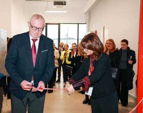
Tirana, November 2025 – Atronix Sh.p.k., Albania’s pioneering Electronics Manufacturing Services company, officially inaugurated in November its new production facility at Tirana Industrial Park. The event marks a historic moment for Albania’s industrial landscape, establishing the country’s first advanced EMS factory with capacity to serve European and North American markets.

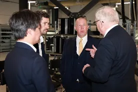
Equipped with the latest generation of JUKI SMT Production line with advanced AOI/X-ray inspection ERSA selective and wave soldering, and fully integrated traceability systems, Atronix introduces advanced technological capabilities. 

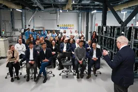
The inauguration ceremony brought together distinguished guests, including leading figures from the European electronics industry Mr. Dieter Weiss, EBRD representatives. Ms. Ekaterina Solovova, Ms. Egla Ballta, JUKI Europe Mr. Kenji Hirohata, Mr. Rui Vidal and Mr. Davor Jakulin international and national business partners, representatives from the Albanian Government, Academia and Universities, etc. 

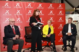
“Our vision from the beginning was clear: to build a factory that stands at the same level with Europe’s most advanced EMS providers,” said Ms. Enkeleda Kuka, Founder & CEO of Atronix. “Today, we are proud to show that Albania can compete in high-precision electronics manufacturing.” During the ceremony, Atronix extended appreciation to its international collaborators, including JUKI Europe, Kurtz-Ersa, and several global clients and advisors who have contributed to the company’s rapid development. 

“In this challenging business climate, it is very good to see a new EMS company being opened in Albania. Eastern Europe will see a strong growth of electronic production in the future and Atronix will participate in this development.” said Mr. Dieter G. Weiss, European EMS industry expert and longstanding supporter of the project. 

This factory sets a new standard for high-value manufacturing in the country and demonstrates how it can transform Albania's industrial landscape. EBRD has supported Atronix through our Advice for Small Business program and looks forward to the future successes of Atronix" said Ms Ekaterina Solovova, Head of Albania, EBRD.

With its inaugural production lines now operational, Atronix is preparing for a strong expansion phase, targeting new partnerships in Electronic Manufacturing and broader industrial integration across Europe and North America. 

“Atronix symbolizes what the next chapter of Albanian industry can look like,” added Ms. Kuka. “We are committed not only to manufacturing high-quality electronics, but also to building trust, reliability, and long-term value for every client who chooses Albania as their production base. 


www.atronix.al[email protected]; Tirana Industrial Park 48, Kashar, Tirana,  Albania

Validation underscores DAS EE’s 35 years of leadership in advanced and sustainable abatement solutions
Dresden, Germany, November 28, 2025 — As the semiconductor industry intensifies its efforts to reach net-zero emissions, the recently published SEMI SCC Whitepaper “Overview of F-GHG and Nitrous Oxide Semiconductor Abatement Technologies” (2024) establishes new industry performance benchmarks for greenhouse gas abatement. The report defines a minimum Destruction and Removal Efficiency (DRE) for CF₄ of >95% and a maximum goal of >99% for process gas abatement systems.

These new reference points represent a significant step beyond the legacy assumptions used in many ESG reports and supplier requirements, which have historically relied on conservative default values for greenhouse gas abatement performance. However, even the upper range of the SEMI SCC targets does not yet represent the full potential of modern technology.

DAS Environmental Expert GmbH demonstrates with its TILIA abatement system that destruction efficiencies exceeding 99.9% for CF₄ and other F-GHGs are both technically feasible and economically advantageous. These systems outperform the benchmarks set forth by the SEMI SCC whitepaper and contribute directly to the industry's carbon reduction goals.

“Systems like TILIA prove that it is not only possible but also economically rational to exceed the current industry benchmarks,” says Stephan Raithel, Chief Operating Officer Gas Treatment at DAS Environmental Expert GmbH. “With rising carbon taxes and tightening sustainability targets, investing in high-efficiency abatement translates directly into operational and financial benefits.”

The global semiconductor industry emits thousands of tons of CF₄ annually, a gas with a Global Warming Potential (GWP) of 7,390. Even a few tons of unmitigated emissions correspond to millions of tons of CO₂ equivalents. While current industry practice aims to meet the SCC-recommended minimum DREs, only systems operating consistently above 99.9% will enable the industry to meet its net-zero commitments.

The SEMI SCC Whitepaper emphasizes that achieving these higher efficiencies is crucial for the industry’s sustainability roadmap and requires broad adoption of next-generation abatement technologies. DAS Environmental Experts’ proven TILIA platform exemplifies this transition – setting a new benchmark for “Best in Class” abatement performance in the semiconductor industry.

About the Company
DAS Environmental Experts Group (DAS Group), headquartered in Dresden, Germany, was founded in 1991 and is now a global organization with subsidiaries on three continents and more than 950 employees worldwide. Over the past three decades, DAS Group has become one of the leading technology and equipment providers for waste gas abatement solutions with a focus on semiconductor industry.
In addition, DAS Group develops advanced process and system solutions for industrial water treatment, with extensive expertise in the recycling and reuse of wastewater from the semiconductor industry.
DAS solutions are engineered to meet the stringent purity requirements of semiconductor manufacturing, helping clients comply with global environmental standards.

New platform delivers ALD film quality at production throughput for Wide Bandgap and other specialty device manufacturing

Espoo, Finland, November 19, 2025 – Beneq, a global leader in Atomic Layer Deposition (ALD) equipment and solutions, today announced Beneq Transmute™, a next-generation ALD platform designed for high-volume semiconductor manufacturing. Engineered for high volume production of Wide Bandgap (WBG) power electronics, advanced RF devices, μLED and other specialty devices, Beneq Transmute™ combines performance, scalability, and cost efficiency in one system.

Atomic precision at manufacturing speed

Beneq Transmute™ extends the performance of the Beneq Transform® XP platform into production environments with Beneq’s proprietary 3-step ALD architecture. By combining plasma pre-treatment, plasma-enhanced ALD (PEALD), and thermal batch ALD, the platform delivers conformal, high-performance dielectric stacks with atomic-level interface control – now at high throughput.

Its flow-uniform 25-wafer chambers, paired with advanced precursor dosing technology, enable rapid cycle times, optimized wafer coverage, and reduced precursor waste – resulting in a low cost of ownership across a broad range of semiconductor applications.

“Beneq Transmute™ represents a major leap forward in making ALD a truly high-volume manufacturing solution,” said Lucas Monteiro, Head of Product at Beneq. “By combining the precision of ALD with throughput and scalability that match production demands, we are giving our customers the ability to produce next-generation Wide Bandgap and RF devices at high throughput and low cost of ownership – with the uncompromised film quality that Beneq is known for.”

Designed for dedicated production requirements

Beneq Transmute™ supports both thermal and plasma-enhanced ALD within a modular cluster architecture that enables dedicated configurations. With up to two transfer chambers and eleven process module slots – including PEALD, Thermal, Buffer, and Preheater – each system can be tailored to match specific customer applications and fab roadmaps while ensuring long-term scalability.

Enabling the next wave of electronics

Beneq Transmute™ directly supports key semiconductor market trends – including the electrification of transport, adoption of renewable energy, 5G and RF communications, data centers and next-generation displays. Its combination of atomic precision and production throughput positions Beneq as a technology enabler for a more efficient, connected, and sustainable future.

About Beneq

Beneq pioneered industrial Atomic Layer Deposition (ALD) with the introduction of the first commercial ALD equipment in 1984. Today, Beneq advances ALD technology adoption and validation with a portfolio that includes Transform®, Transform® 300, and Prodigy™ for specialty semiconductor device fabrication; TFS 200 and TFS 500 for R&D; and innovative spatial ALD platforms such as the C2R™ and Genesis for rolltoroll processing. Beneq’s systems support process innovation from lab to fab, enabling integration of ALD in advanced manufacturing. Headquartered in Espoo, Finland, Beneq operates globally to help customers scale ALD solutions for the future of semiconductors, optics, and functional coatings.

Press Contact:
Charlotte Bärlund
Event and Communications Lead
[email protected]

New SECS-II library helps fabs and OEMs integrate semiconductor tools with the MES in hybrid manufacturing sites, ensuring faster time to market and limiting integration costs

MUNICH, November 18, 2025 – Agileo Automation, a leading provider of control and connectivity solutions for global semiconductor manufacturing, today unveils Agil’SECS-II at Booth #C2518 at SEMICON Europa 2025. This new SECS-II library, featuring built-in SEMI standard communication, enables a manufacturing execution system (MES) to accelerate the integration and validation of hybrid semiconductor and traditional manufacturing tools on production lines, ensuring faster time to market, lower integration costs, and reduced deployment risks. With this connection gateway, users can send and receive any SEMI SECS-II-compliant message as host or equipment for full GEM and GEM300 equipment integration and validation. This product can prove valuable for a variety of customers:

• Pure semiconductor original equipment manufacturers (OEMs) that need a practical way to develop an MES simulator and exercise their equipment under fab-like conditions. For small production lines or multi-tool set-ups exchanging data through SECS/GEM, Agil’SECS-II allows OEMs to design, test, and validate their equipment efficiently before shipping it to fabs.

• Customized, multi-industry, or low-volume production sites that use an MES system to integrate both traditional production machines and semiconductor tools. Agil’SECS-II simplifies integration in mixed equipment environments, especially where the MES cannot use SECS/GEM because most tools rely on protocols such as OPC UA, Modbus, or MQTT, yet semiconductor equipment using SECS/GEM must be integrated within the same MES.

• Laboratories and pilot lines without a full-featured MES that require a driver to collect data from various types of manufacturing equipment, including process, inspection, and metrology tools, to ensure quality and process control as well as complete traceability.

“With Agil’SECS-II, we wanted to provide a flexible tool that can serve multiple types of customers who can benefit from a proven software foundation built on more than 15 years of deployment experience in semiconductor fabs worldwide,” explains Marc Engel, chief executive officer of Agileo Automation. “Our SECS-II driver is especially useful for validating the processes of hybrid fabs that combine semiconductor and non-semiconductor manufacturing equipment, such as silicon carbide (SiC) wafer production lines or advanced packaging lines. It enables product and process traceability with legacy MES and helps OEMs developing equipment for these lines create MES simulators to verify information flow between tools using heterogeneous communication protocols.”

- ends -

About Agileo Automation
Agileo Automation is a trusted partner for equipment manufacturers, helping them build smarter, automated, and more connected machines that integrate seamlessly into advanced semiconductor fabs. Founded in 2010 in Poitiers, France, Agileo Automation helps OEMs optimize control, communication, data acquisition, and testing across their tools through proven software frameworks, applications, and expert support. Its flagship A²ECF-SEMI framework provides a solid foundation for developing equipment controllers fully aligned with SEMI SECS/GEM, GEM300, and EDA standards. As an active member of SEMI and the OPC Foundation, Agileo Automation contributes directly to shaping the standards that drive Industry 4.0 manufacturing. For more information, please visit our website or follow us on LinkedIn.

RENA Technologies marks a new milestone in the semiconductor industry with the launch of Vanguard, a state-of-the-art, fully automated single-wafer platform designed for wet chemical cleaning, etching, and drying of 200mm and 300mm wafers. Engineered for performance, efficiency, and scalability, Vanguard offers new possibilities for advanced semiconductor manufacturing.


Broaden the Possibilities in Wafer Wet Processing

Vanguard is purpose-built to address the rising demands of next-generation semiconductor substrates and materials. Supporting 4 to 8 independent processing chambers within a compact footprint, the system delivers high throughput without compromising cleanroom space. Its advanced chemical cleaning and double-sided processing—handling up to five distinct chemistries—minimizes contamination, substrate damage, and defects, ensuring wafers meet the stringent yield and quality requirements of cutting-edge chip manufacturing.

"With the launch of our new semiconductor wet processing platform, we are entering a new aera in precision, efficiency, and reliability for advanced chip manufacturing. This machine embodies our commitment to innovation—delivering not only superior process control but also the flexibility our customers need to stay ahead in a rapidly evolving industry. It represents a decisive step in enabling the next generation of semiconductor technologies for both high-volume manufacturing lines and R&D fabs." Emphasizes Peter Schneidewind, CEO of RENA Technologies.

Scalable, Modular Design 

Vanguard’s modular architecture grows with customer needs. Fabs can easily adjust chamber count and process configurations to match evolving requirements, from R&D to high-volume production.
The platform integrates internal chemistry preparation for precise formulation control, ensuring consistent process delivery and minimizing chemical consumption. This reduces operating costs and environmental impact—key considerations for sustainable fabs.


Serviceability is also built-in: each chamber operates independently, allowing maintenance without halting production. Combined with AI-assisted process control, and the digital service platform RENA Connect Hub, customers gain maximum uptime and efficiency.


Next-Level Automation and Compatibility

With its digital twin simulation, customers can model system integration, test interfaces, and even simulate throughput with real process data—well before installation. Training and upgrades can be conducted seamlessly during live production.

Fully GEM300 compatible, Vanguard is integration-ready from day one. Operating within a Class 1 mini environment, it guarantees ultra-clean wafer handling, while its advanced drying ensures residue-free, pristine surfaces for downstream processing.


Key Features at a Glance

  • Fully automated wet processing for 200mm / 300mm wafers
  • Scalable from 4 to 8 single-wafer chambers
  • Double-sided cleaning with up to 5 chemicals
  • Internal chemistry preparation system
  • AI-assisted software with predictive maintenance
  • Advanced drying technology
  • Class 1 mini environment for ultra-clean operation
  • Compact footprint with high-throughput capability
  • GEM300 factory-integration ready
  • Low chemical usage for reduced cost and environmental impact 

Availability

Vanguard is officially available as of today. Semiconductor fabs and foundries seeking to modernize their wet processing capabilities now have access to a solution that combines performance, scalability, and sustainability—delivered today for the challenges of tomorrow.

OXFORD INSTRUMENTS PROVIDES COHERENT WITH STATE-OF-THE-ART, FULLY AUTOMATED PROCESSING EQUIPMENT, FOR 6” INP WAFER MANUFACTURING, ENABLING NEXT GENERATION AI APPLICATIONS

Oxford Instruments (OXIG), a leading provider of advanced plasma processing solutions for the compound semiconductor industry, announces the key role it is playing to support the industry’s first fully automated 6-inch indium phosphide (InP) wafer fabrication capability for photonic devices, led by Coherent Corp. (NYSE: COHR), a global leader in compound semiconductors and high-performance optical networking solutions.

Oxford Instruments’ cutting-edge plasma processing equipment is central to Coherent’s groundbreaking achievement of ramping up 6-inch InP fabs in Sherman, Texas, and Järfälla, Sweden. These fabs will play a pivotal role in driving advancements in AI datacentre, telecommunications, and sensing applications. Coherent’s transition to 6-inch wafers is set to deliver significant benefits, including a substantial increase in capacity, lower die cost and more than four times the number of devices per wafer.

Oxford Instruments has supplied fully automated, high-throughput 6-inch InP processing equipment, enabling Coherent to achieve these remarkable productivity gains. This advanced equipment is designed to support the transition from 800G to 1.6T products, a key requirement to meet the growing demands of AI interconnects and optical communications.

“We have been the leading supplier of InP plasma etch equipment to the datacom market, and Coherent, for many years. Our technology, with the quality, throughput and reliability that we have developed alongside excellent service, is ideally positioned to support the current device demand inflection we are seeing with the release of generative AI applications. We are delighted to be partnering with Coherent during this exciting period of market expansion and look forward to continuing to develop and release innovative and valuable plasma processing solutions.” Matt Kelly, Managing Director, Oxford Instruments Plasma Technology.

"Coherent’s move to 6-inch InP wafer fabrication marks a transformative milestone for the industry. Oxford Instruments’ expertise in plasma processing has been essential in enabling our Sherman and Järfälla fabs to reach world-class performance,” said Dr. Beck Mason, Executive Vice President – Semiconductor Devices at Coherent. “Together, we are advancing InP technology to support faster networks, greater efficiency, and the new applications that will define the future of connectivity."

The joint efforts of Oxford Instruments and Coherent have culminated in a manufacturing platform that sets the stage for the next generation of InP optoelectronic devices. These devices are critical enablers for applications ranging from AI datacentres and datacom transceivers to advanced sensing in consumer electronics and automotive technologies.

Belgium France Germany Ireland Italy Japan Malaysia Singapore South Korea Taiwan United States Register Now ripple effect webinar 2 Business Executive
Highlighted content

United States

Sustainability

Join SEMI and the Environment Risk & Mitigation Reporting Working Group to learn how the semiconductor industry and supply chain is assessing Water Risk, and what steps can be taken to mitigate exposure. 

In a collaboration with WaterPlan®, the working group surveyed more than 140 production site and 89 unique water basins to arrive at a water risk assessment for flooding, reputational risk, water quality risk, infrastructure risk and water scarcity risk. The survey found that over 80% of wafer fabrication and 88% of chemical and materials sites face medium-high to high flood risk.

During the webinar experts will provide key insights on key drivers and what is required by risk management teams – both internal and external – for reports and disclosures for:

  • The Global Reporting Initiative (GRI)
  • Disclosure Insight Action (CDP)
  • Task force on Climate-Related Financial Disclosures (TCFD)
  • The International Sustainability Standards Boards (ISSB)
  • Sustainability Accounting Standard Board (SASB)
  • European Sustainability Reporting Standards (ESRS)

Register now to learn more.

8:00 am - 9:00 am Off Add to Calendar 2025-12-11 08:00:00 2025-12-11 09:00:00 Ripple Effects: Water Risk and Resilience Join SEMI and the Environment Risk & Mitigation Reporting Working Group to learn how the semiconductor industry and supply chain is assessing Water Risk, and what steps can be taken to mitigate exposure. In a collaboration with WaterPlan®, the working group surveyed more than 140 production site and 89 unique water basins to arrive at a water risk assessment for flooding, reputational risk, water quality risk, infrastructure risk and water scarcity risk. The survey found that over 80% of wafer fabrication and 88% of chemical and materials sites face medium-high to high flood risk.During the webinar experts will provide key insights on key drivers and what is required by risk management teams – both internal and external – for reports and disclosures for:The Global Reporting Initiative (GRI)Disclosure Insight Action (CDP)Task force on Climate-Related Financial Disclosures (TCFD)The International Sustainability Standards Boards (ISSB)Sustainability Accounting Standard Board (SASB)European Sustainability Reporting Standards (ESRS)Register now to learn more. United States SEMI.org [email protected] America/Los_Angeles public America/Los_Angeles
Event format
Promote in calendar
On

San Diego, CA and Hsinchu, TaiwanOctober 27, 2025 ElevATE Semiconductor, a leader in high-density, low-power, pin electronics (PE) and device power supplies (DPS), voltage/current sources (VI), and parametric measurement units (PMU) solutions, is excited to announce the opening of its first office in Hsinchu, Taiwan. The new location will strengthen support for customers and partners across Asia through localized engineering expertise and closer collaboration. 

The facility will serve as a regional hub for sales, applications, and quality and failure analysis engineering, enabling ElevATE to deliver direct and high-speed support to its growing customer base. ElevATE’s corporate headquarters and production operations will remain in San Diego, ensuring customers worldwide continue to receive the same quality, reliability, and responsiveness they rely on today.  

Located in the heart of Taiwan’s semiconductor ecosystem, the Hsinchu office underscores ElevATE’s commitment to building close relationships with regional customers, accelerating support, and driving adoption of its advanced test IC solutions. 

“Opening an office in Hsinchu is an important step for us,” said Johnny Chung, Asia Sales Manager at ElevATE Semiconductor. “It gives us a stronger local presence and lets us work closely with customers in their time zone. By adding this office to the resources we already have in Asia, we can respond faster and support our partners more effectively.” 

As ElevATE expands its geographic footprint, the company also plans to grow its Taiwan team with key hires in applications and quality and failure analysis engineering. These roles will complement its U.S.-based teams to enhance global coverage and help drive adoption of ElevATE’s next generation test IC solutions worldwide. 

This expansion is part of ElevATE’s long-term strategy to strengthen its global presence and invest in the future of semiconductor test technology, empowering customers to bring next-generation test systems and instruments to market with confidence.  

About ElevATE Semiconductor ElevATE is a leader in high-performance IC design for the automated test equipment (ATE) industry. The company is committed to supporting the semiconductor and system test community by providing advanced integrated circuits (ICs) that address the complex challenges of ATE. With a focus on designing efficient, high-density solutions, ElevATE aims to reduce the overall cost of testing for its customers, both now and in the future. For more information, visit www.elevatesemi.com 

Registration

For questions, please contact [email protected]

Belgium France Germany Ireland Italy Japan Malaysia Singapore South Korea Taiwan United States Vietnam Image Business Training Featured Speakers

Leverage SEMI U learning offerings to accelerate your professional development journey for 2026! Our pledge remains unwavering: providing comprehensive, technical education to equip you with the skills needed for a prosperous journey in the semiconductor sector.

Are you ready to take your semiconductor industry knowledge to the next level? We're thrilled to invite you to our upcoming webinar titled "Kick Start 2026 with SEMI U." This webinar promises to be an informative session where you'll gain insights into the latest updates and course offerings. 

During this webinar, you can expect to:  

  • Discover the latest updates and enhancements to SEMI U's on-demand course catalog.  
  • Upcoming virtual and in-person instructor-led trainings scheduled for the first half of the year.
  • Gain access to a special 10% discount on ALL on-demand courses.  


United States

Headshot of Naresh Naik
Naresh Naik
Director, SEMI University
SEMI
SEMI U Workforce Development

Join us to discover our current course offerings, upcoming in-person and virtual trainings, and more. Engage in a Q&A session. Plus, by attending this free webinar, you'll receive a 10% discount code for all on-demand courses and will be entered into a raffle to win a FREE course bundle ($100 value).

5:00 pm - 5:30 pm Off Add to Calendar 2026-01-21 17:00:00 2026-01-21 17:30:00 Kick Start 2026 with SEMI U - Free Webinar (PM Session) Join us to discover our current course offerings, upcoming in-person and virtual trainings, and more. Engage in a Q&A session. Plus, by attending this free webinar, you'll receive a 10% discount code for all on-demand courses and will be entered into a raffle to win a FREE course bundle ($100 value). United States SEMI.org [email protected] America/Los_Angeles public Register Now
Event format
Promote in calendar
Off

Registration

For questions, please contact [email protected]

Belgium France Germany Ireland Italy Japan Malaysia Singapore South Korea Taiwan United States Vietnam Image Business Training Featured Speakers

Leverage SEMI U learning offerings to accelerate your professional development journey for 2026! Our pledge remains unwavering: providing comprehensive, technical education to equip you with the skills needed for a prosperous journey in the semiconductor sector.

Are you ready to take your semiconductor industry knowledge to the next level? We're thrilled to invite you to our upcoming webinar titled "Kick Start 2026 with SEMI U." This webinar promises to be an informative session where you'll gain insights into the latest updates and course offerings. 

During this webinar, you can expect to:  

  • Discover the latest updates and enhancements to SEMI U's on-demand course catalog.  
  • Upcoming virtual and in-person instructor-led trainings scheduled for the first half of the year.
  • Gain access to a special 10% discount on ALL on-demand courses.  


United States

Headshot of Naresh Naik
Naresh Naik
Director, SEMI University
SEMI
SEMI U Workforce Development

Join us to discover our current course offerings, upcoming in-person and virtual trainings, and more. Engage in a Q&A session. Plus, by attending this free webinar, you'll receive a 10% discount code for all on-demand courses and will be entered into a raffle to win a FREE course bundle ($100 value).

8:00 am - 8:30 am Off Add to Calendar 2026-01-21 08:00:00 2026-01-21 08:30:00 Kick Start 2026 with SEMI U - Free Webinar (AM Session) Join us to discover our current course offerings, upcoming in-person and virtual trainings, and more. Engage in a Q&A session. Plus, by attending this free webinar, you'll receive a 10% discount code for all on-demand courses and will be entered into a raffle to win a FREE course bundle ($100 value). United States SEMI.org [email protected] America/Los_Angeles public Register Now
Event format
Promote in calendar
Off