downloadGroupGroupnoun_press release_995423_000000 copyGroupnoun_Feed_96767_000000Group 19noun_pictures_1817522_000000Member company iconResource item iconStore item iconGroup 19Group 19noun_Photo_2085192_000000 Copynoun_presentation_2096081_000000Group 19Group Copy 7noun_webinar_692730_000000Path
Skip to main content
Default Banner Image

China

FREMONT, Calif. – June 14, 2021 – YES (Yield Engineering Systems, Inc.), a leading manufacturer of process equipment for semiconductor advanced packaging, life sciences and “More-than-Moore” applications, today announced that it has become a member of the Silicon Saxony industry association. YES, which recently established a German presence in Dresden, expects the high-tech networking group to be a valuable resource in marketing advanced process equipment and solutions to an expanding customer base across Europe, particularly in Germany. In addition, the company plans to strengthen communication and alliances with fellow members of Silicon Saxony.

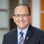
“Silicon Saxony brings together companies that are leading the electronics industry in Europe,” said Dragan Cekic, YES’s Vice President of Sales for Europe and the Americas. “We are excited to join their ongoing conversation about trends and technologies that will affect us all.”
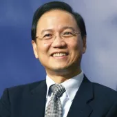
“Change is a given in the markets we serve. The opportunities facing our industry are complex, and the rapid pace of technological developments is unprecedented. We look forward to participating in Silicon Saxony’s high-tech network with the aim of addressing today’s exciting semiconductor roadmaps,” said Rezwan Lateef, President of YES.

About YES
YES (Yield Engineering Systems, Inc.) is a preferred provider of high-tech, cost-effective equipment for transforming surfaces, materials and interfaces. The company’s product lines include vacuum cure systems, chemical vapor deposition (CVD) systems, and plasma etching tools used for precise surface modification and thin-film coating of semiconductor wafers, semiconductor and MEMS devices, biosensors and medical substrates. With YES, customers ranging from startups to Fortune 100 companies can create and volume-produce products in a wide range of markets, including Advanced Packaging, MEMS, Augmented Reality/Virtual Reality and Life Sciences. YES is headquartered in Fremont, California, with a growing presence globally. For more information, please visit www.yieldengineering.com.

About Silicon Saxony
With more than 350 members, Silicon Saxony e. V. is the largest high-tech network in Saxony and one of the largest microelectronics and IT clusters in Germany and Europe. Founded in 2000, Silicon Saxony is a self-financed association linking manufacturers, suppliers, service providers, universities, research institutes, public institutions as well as industry-relevant start-ups. Its focus is on the technological trends of the present and future: artificial intelligence, robotics, automation, Internet of Things, sensor technology, energy efficiency, and neuromorphic and edge computing. As a high-profile information, communication and cooperation platform, the association promotes the regional, national and international networking of its members by participating in and organizing industry events.

IC’Alps Builds a Secure Infrastructure for Ultimate Protection of Customers’ Data

Meylan, FRANCE – June 08, 2021 – In wake of the recently announced partnership with Tiempo Secure for silicon implementation of CC (Common Criteria) EAL5+ grade Secure Element IP, IC’Alps has deployed an infrastructure that complies with the highest security standards.

IC’Alps is a French semiconductor company specializing in the design and supply of exclusive and custom-made ASIC solutions (Application Specific Integrated Circuits). As part of the improvements, the company has set up a secure access management system including premises complementary access control, dedicated and secure design room, and an isolated and secure IT network. This revamp increases the security in IC’Alps’ Head Office as demanded by security-sensitive customers or partners, requiring such a high level of data protection and associated traceability.

IC’Alps successfully passed CC audit of secure room and associated IT infrastructure commissioned by Tiempo Secure, audit performed by a security evaluation labs (ITSEF) licensed by the ANSSI. The audit states that the silicon physical implementation work entrusted by Tiempo Secure to IC’Alps passed the very strict requirements.

“Since the company was founded, IC’Alps has invested significant financial and human resources into IT. We are proud to pass this CC audit for this customer’s project. This is an independent recognition of our commitment to providing the highest level of quality, data security and customer service”, said Jean-Luc Triouleyre, CEO of IC’Alps.

In addition to ISO 13485 (medical) and EN 9100 (aeronautics) certifications, joining an elite group of companies providing a design environment complying with the highest security standards, will strengthen IC’Alps’ business opportunities for silicon implementation of custom chips and hard macros targeted for security-sensitive markets such as, but not limited to, banking, defence, government and implantable medical devices.

ABOUT IC’ALPS
IC’Alps is your one-stop-shop ASIC partner. The company provides customers with a complete offering for Application Specific Integrated Circuits (ASIC) and Systems on Chip (SoC) development from circuit specification, mastering design in-house, up to the management of the entire production supply chain. From its technical centre in France (Grenoble area), IC’Alps supports multiple projects in the demanding medical, industrial, transport, IoT, and mil/aero sectors. The highly qualified engineering teams cover every expertise needed and have a long experience of on-demand analog, mixed-signal and digital integrated circuits on technologies from 0.35 µm down to 16 nm. Moreover, IC’Alps has a proven track record of success with sensor/MEMS AFE interfaces, low power consumption designs, high-resolution converters, signal processing, multiprocessors architectures, hardware accelerators, to name a few. Being a partner of major semiconductor foundries, IP providers, as well as packaging and test houses, IC’Alps is well placed to support customers with full life-cycle solutions. We are proud to be Arm® approved Design Partner, a member of X-FAB’s design and supply chain partner network, as well as an Imec IC-link partner. These accreditations assure that we provide expert support and that we have the design expertise to create highly innovative ASIC designs. IC’Alps is ISO 9001, ISO 13485, EN 9100 certified, as well as Common Criteria ready. More information can be found at www.icalps.com

An opportunity to boost development for Additive Manufacturing & Semicon industry.

Inventec Performance Chemicals, a global provider of Soldering, Cleaning & Coating solutions, acquired PUS (Pure Ultrasonic System) in April 2021. PUS’ main activities are the production of equipment (solder powder atomizers and sieving machines) and the production of solder powders, from its own process.

By acquiring PUS, Inventec saw an opportunity to create a synergy in the additive manufacturing industry. Inventec supplies the 3D market for high-tech application, with its cleaning, particle elimination & finishing products, while PUS provides sieving, recycling and depowdering, to provide a circular economy solution for this fast-developing market.

Furthermore, the addition of PUS will strengthen Inventec’s know-how in metallurgy, for the development of solder pastes, with ultrafine powders and specialty alloys for the semicon industry. Adapting to an evolving industry, this acquisition allows Inventec to innovate and meet worldwide customers’ needs.

ABOUT INVENTEC
INVENTEC PERFORMANCE CHEMICALS is a global provider of soldering, cleaning & coating materials for electronic, semiconductor and industrial applications.

For more than 50 years we have shown leadership in innovation by putting environment & health impact, sustainability and reliability at the core of our product development.

With iso 9001 & 14001 production sites in France, Switzerland, USA, Mexico, Malaysia and China we can guarantee a smooth and cost-effective supply chain. On top of this, all our production facilities are equipped with a cleaning application centre, where customers are invited to test our proposed cleaning solutions.

Inventec supplies to many industries and the excellent performance of our products in applications demanding high reliability, leads us to focus especially on the automotive, aerospace, semiconductor, automation & energy and medical industry.
For more information about Inventec Performance Chemicals, visit https://www.inventec.dehon.com/en/

ABOUT PUS
PURE ULTRASONIC SYSTEMS is a French expert for ultrasonic atomization and ultrasonic sieving. At its creation, PUS first specialized in atomization and sieving equipment, manufacturing devices for ultrasonic atomization of solder powder for electronic assembly. 10 years later, PUS is still innovating to develop new equipment and powders for the Additive Manufacturing Market.
For more information about PUS, visit https://www.pus-net.fr/en/

ESPOO, Finland, 2nd of June 2021 – Picosun Group has pending patent rights for an ALD enabled corrosion protection solution against plasma etch that will bring benefits in semiconductor fabrication processes in terms of throughput, film uniformity and conformality. With PicoArmour(TM) the corrosion protection can be achieved more efficiently compared with the industry solutions commonly used today.

Wafer fabrication process flows include several steps where plasma etching is necessary. An inevitable consequence of using etching chemicals is that the tool itself will be etched. A common industrial solution for reducing the tool damage is applying a corrosion-resistant coating to the etch tool using for example PVD or spray coating with Y2O3. Compared to only using Y2O3, PicoArmour(TM) enables an up to five times faster and a more cost-effective way of producing the coating. Compared to Al2O3, the coating can be five times more durable.* Also, the maintenance interval of etch tools can be increased which also translates to significant reduction of manufacturing costs.

“Picosun’s approach with PicoArmour(TM) is to combine the highly-etch-resistant Y2O3 ALD process with more robust ALD processes. A high performance ALD corrosion barrier combining the speed and convenience of Al2O3 process with the durability of Y2O3 can be achieved by carefully controlling the film composition. With ALD, the protective effect can be achieved with thinner films, which in turn leads to material savings and a more environmentally friendly process”, states Juhana Kostamo, VP, Industrial Business Area of Picosun Group.

To learn more about PicoArmour(TM) and a study Picosun has done related to protective coatings against plasma damage, join Picosun talk at the virtual ALD 2021 conference on June 29 at 10:25 am EDT.
Register here: https://ald2021.avs.org/register/

*Values dependent on deposition and etch parameters

About Picosun
Picosun provides the most advanced AGILE ALD® (Atomic Layer Deposition) thin film coating solutions for global industries. Picosun’s ALD solutions enable technological leap into the future, with turn-key production processes and unmatched, pioneering expertise in the field – dating back to the invention of the technology itself. Today, PICOSUN® ALD equipment are in daily manufacturing use in numerous leading industries around the world. Picosun is based in Finland, with subsidiaries in Germany, USA, Singapore, Japan, South Korea, China mainland and Taiwan, offices in India and France, and a world-wide sales and support network. Visit www.picosun.com.

More information:
Juhana Kostamo
Vice President, Industrial Business Area, Picosun Group
Tel: +358 50 369 9565
Email: [email protected]
www.picosun.com

YES (Yield Engineering Systems, Inc.), a leading manufacturer of process equipment for semiconductor advanced packaging, life sciences and “More-than-Moore” applications, today announced a strategic alliance with SPEC (Semiconductor Process Equipment Corporation) of Valencia, California. Under the terms of the agreement, YES will market, distribute and support SPEC’s cleaning, etching, stripping and plating equipment worldwide. Furthermore, YES plans to expand SPEC’s process expertise by investing in technologists and demo capabilities to help customers implement faster cycles of learning. In addition, YES and SPEC expect to develop a variety of new products drawing on each other’s core technical expertise.

The agreement leverages the strengths of both companies to meet the growing demands of emerging markets such as 5G, autonomous driving, augmented reality, and other computationally-intensive applications.

“In bringing together our two companies’ combined seven decades of engineering and process development expertise, YES will create new process technologies for a variety of semiconductor, life science and optical coating applications, and will offer broader, more complete integrated solutions to our customers,” said Rezwan Lateef, President of YES.

“We look forward to combining our knowledge base with YES’s large and ever-growing repository of process expertise to address customer needs,” said Kevin McGillivray, co- founder of SPEC. “In addition, YES’s established global sales and service network will enable more companies around the world to utilize SPEC’s cost-effective, production-proven automated wet-process solutions.”

About YES
YES (Yield Engineering Systems, Inc.) is a preferred provider of high-tech, cost-effective equipment for transforming surfaces, materials and interfaces. The company’s product lines include vacuum cure systems, chemical vapor deposition (CVD) systems, and plasma etching tools used for precise surface modification and thin-film coating of semiconductor wafers, semiconductor and MEMS devices, biosensors and medical substrates. With YES, customers ranging from startups to Fortune 100 companies can create and volume-produce products in a wide range of markets, including Advanced Packaging, MEMS, Augmented Reality/Virtual Reality and Life Sciences. YES is headquartered in Fremont, California, with a growing presence globally. For more information, please visit http://www.yieldengineering.com.

About SPEC
SPEC (Semiconductor Process Equipment Corporation) is a highly experienced supplier of surface conditioning wet process equipment. Since 1986, SPEC has designed and manufactured wafer-level and device-level wet process equipment for acid and solvent surface modification (cleaning, etching, stripping), electroplating, and electroless (chemical) plating for all industries requiring a high level of process cleanliness. SPEC’s products are used for polysilicon chip, chunk and ingot cleaning; crucible cleaning, cavity cleaning for particle accelerators, chemical mixing and delivery, hard drive component cleaning, and quartzware cleaning. SPEC systems are engineered to match the unique requirements of the end user. For more information, please visit http://www.team-spec.com.

The IOSS WID120 Wafer ID Reader is the latest generation of advanced Wafer ID Readers. It was designed to close the gap between easy usability and highest flexibility. With up to 18 different light modes, the IOSS WID120 decodes OCR, Barcode, DataMatrix and QR-Code markings on any kind of wafer, regardless of the wafer material. Thanks to its fully automatic light control and intelligent configurations handling, the IOSS WID120 is able to tweak itself and improve your read rates drastically. The guided teaching process makes it very easy for everyone to setup the camera. Already known functions as master/slave functionality and database connection are still available with this new model. Picture export via FTP is now also possible.

The Electronic System Design (ESD) Alliance, a SEMI Technology Community, today welcomed back nine members of its Governing Council along with newly elected member Aki Fujimura, D2S’ CEO.

Simon Segars, CEO of Arm, continues as the Governing Council chair.

Returning Governing Council members who will serve a two-year term that runs through 2023:
• Dr. Aart de Geus, chairman and co-CEO of Synopsys, Inc.
• Dean Drako, president and CEO at IC Manage
• Dr. John Kibarian, president and CEO of PDF Solutions, Inc.
• Prakash Narain, president and CEO from Real Intent
• Joe Sawicki, executive vice president of Siemens EDA
• Simon Segars, CEO of Arm
• Babak Taheri, CEO/CTO of Silvaco
• Lip-Bu Tan, CEO of Cadence Design Systems
• Bob Smith, executive director of the ESD Alliance

“It’s a pleasure to welcome back members of our Governing Council and new member Aki Fujimura,” remarks Smith. “We accomplished a great many items on our goals list for the last term and I look forward to completing even more in the new term.”

The current slate of Governing Council members was elected by more than 90% of eligible members companies casting ballots during the voting period that ended May 14.

About the Electronic System Design Alliance
The ESD Alliance, a SEMI Technology Community, is the central voice to communicate and promote the value of the semiconductor design ecosystem as a vital component of the global electronics industry. As an international association of companies providing goods and services throughout the semiconductor design ecosystem, it is a forum to address technical, marketing, economic and legislative issues affecting the entire industry.

Follow the ESD Alliance
www.semi.org/en/communities/esda
ESD Alliance Bridging the Frontier blog
Twitter: @ESDAlliance
LinkedIn
Facebook

All trademarks and registered trademarks are the property of their respective owners.

microCETI™ supports all laser processes in microLED display manufacturing with up to several orders of magnitude higher transfer rates; multiple system orders already received

Chemnitz, Germany, May 12, 2021—3D-Micromac AG, the industry leader in laser micromachining and roll-to-roll laser systems for the semiconductor, photovoltaic, medical device and electronics markets, today introduced microCETI™—the first laser micromachining platform that supports all laser processes in microLED display manufacturing with the high throughput and precision, and low cost of ownership, needed for volume production requirements.

The microCETI platform is available in three different configurations, enabling cost-effective transfer, lift-off and repair of microLED devices. Its high speed enables the transfer of hundreds of millions of microLEDs per hour without having to apply mechanical forces – up to several orders of magnitude faster than other approaches – while the on-the-fly square-beam laser enables transfer of nearly any shape and size of microLED. 3D-Micromac has already received multiple system orders for the microCETI platform from leading microLED chip manufacturers in North America and Asia for laser lift-off and transfer processing.

A Promising Display Technology Enabled By Laser Micromachining
MicroLEDs have the potential to revolutionize the display industry, promising a variety of advantages such as superior viewing angle, high dynamic range with perfect black luminance and high brightness, wide color gamut, fast refresh rates, long lifetime and low power consumption. However, the microLED fabrication process is vastly more complex than LCD and OLED manufacturing, and faces several technical challenges that must be overcome before microLEDs can be readily available in the mass market.

Among these challenges is detaching and transferring the processed microLED chips from the donor or growth (e.g., sapphire) substrate to an intermediate substrate for subsequent testing, allowing the expensive growth substrate to be repurposed for future use. Another challenge is to quickly and precisely transfer the chips to the final glass backplane, which for a typical 4K display involving tens of millions of microLED chips could take hundreds of hours using traditional pick-and-place transfer methods. Technologies are also needed that can detect and repair/replace defective microLEDs during the manufacturing process, since a pixel yield rate of 99.9999 percent is required to produce a full-HD desktop display. The microCETI platform from 3D-Micromac supports all laser processes in microLED display manufacturing, with the ability to address precisely these challenges.

According to Uwe Wagner, CEO of 3D-Micromac, “MicroLEDs have enormous potential for future displays across a wide range of applications and end devices, including indoor and outdoor signage, smart watches, augmented and virtual reality headsets, and automotive heads-up displays. As a leader in laser micromachining, 3D-Micromac has extensive experience applying innovative laser technology to new and emerging applications to support their volume-production requirements. Our new microCETI platform provides a high-throughput, versatile and cost-effective laser micromachining process that is ideally suited for the production of microLEDs. We look forward to working with microLED device and display manufacturers to accelerate the adoption of this exciting and promising display technology.”

The microCETI platform is available in one of three configurations:
• LIFT: unique laser transfer process for nearly every microLED material and shape
• LLO: on-the-fly laser lift-off suitable for customer related microLED material
• REPAIR: Single-die-repair process at every step of the microLED production route

The microCETI platform features a high-precision UV-wavelength laser with high repetition rate and an advanced positioning system for three stages (donor stage, substrate stage and mask stage) and up to 16 axes to transfer every microLED with sub-two-micron positioning accuracy and nanometer-scale repeatability. microCETI supports donor wafer sizes ranging from 50mm (2 inches) up to 200mm (8 inches) as well as intermediate/transfer wafers and backplane substrates up to 350mm x 350mm. In addition to microLEDs, the microCETI platform is also suitable for standard LED and miniLED processing.

Product Availability and Further Information
3D-Micromac is currently accepting orders for the microCETI platform. More information on microCETI, including our latest white paper “Laser technologies for microLED production,” can be found at https://3d-micromac.com/laser-induced-forward-transfer/microceti-lift/.

About 3D-Micromac
Founded in 2002, 3D-Micromac AG is the industry leader in laser micromachining, delivering powerful, user-friendly and leading-edge processes with superior production efficiency. We develop processes, machines and turnkey solutions at the highest technical and technological level. 3D-Micromac systems and services have been successfully implemented in various high-tech industries worldwide including photovoltaic, semiconductor, glass and display industries, micro diagnostics, and medical technology. For more information, visit the company’s website at http://www.3d-micromac.com.

ESPOO, Finland, 19th of May 2021 – Picosun Group has further optimized its PICOSUN® Sprinter ALD system processes successfully for semiconductor, display and IoT component manufacturing lines.

PICOSUN® Sprinter ALD system Al2O3 process results showed excellent thickness uniformity even at low 90 °C deposition temperature. At 300 °C temperature the results were at record-breaking level (About Picosun
Picosun provides the most advanced AGILE ALD® (Atomic Layer Deposition) thin film coating solutions for global industries. Picosun’s ALD solutions enable technological leap into the future, with turn-key production processes and unmatched, pioneering expertise in the field – dating back to the invention of the technology itself. Today, PICOSUN® ALD equipment are in daily manufacturing use in numerous leading industries around the world. Picosun is based in Finland, with subsidiaries in Germany, USA, Singapore, Japan, South Korea, China mainland and Taiwan, offices in India and France, and a world-wide sales and support network. Visit www.picosun.com.

More information:
Juhana Kostamo
Vice President, Industrial Business Area, Picosun Group
Tel: +358 50 369 9565
Email: [email protected]
Web: www.picosun.com

REGISTRATION DETAILS

Registration Includes:

  • Access to recordings and presentations

Member Price: $199

Non-Member Price: $219

Non-Member Price for Government, Military, and Academia: $199 
Contact Michelle Fabiano at [email protected] for discount code. Must have a valid .gov, .mil or .edu or email address

Non-Member Price for Students: $199 
Contact Michelle Fabiano at [email protected] for discount code. Must have a valid student identification card.

Belgium China France Germany Ireland Italy Japan Malaysia Russia Singapore South Korea Taiwan United States Vietnam Register Now Log Into Symposium Medtech main 300w.jpg Business Executive Technical

Media Sponsors

www.healthtechinsider.com
Highlighted content

Bridging the Gap Between Engineering and the Life Sciences

OVERVIEW

The Symposium brought together experts to share their work and identify gaps to accelerating the development of technologies and optimize health outcomes.  Topics covered included using AI in diagnostics and decision-making using AI; data fusion for real time diagnosis; and the impact of these technologies on rural and decentralized healthcare.

Layered on top was the topic of performance augmentation by reading biochemical markers, digital genomics, using new and proposed bio-sensors and wearables.  We heard about tools and technologies available to assess physiological markers that are correlated to health and wellness such as stress, fatigue, chronic disease and cognition. 

The forum focused on bringing together the players across the growing range of industries that are advancing human monitoring applications to:

  • share pre-competitive ideas that may be applied to product development
  • assess roadblocks in bringing human monitoring products to market
  • form partnerships that have become key in overcoming obstacles to successful manufacturing and product development

Symposium Planning Committee

  • Michael Brothers, PhD, UES
  • Dr. Andreas Caduff, Digital Medicine Society
  • Dr. Paul Chao, National Chiao Tung University
  • Caroline Desvergne, PhD, CEA-Leti
  • Doyle Edwards, Brewer Science
  • Dr. Johnsee Lee, Personal Genomics
  • Dr. Yi-Shao Liu, Helios Bioelectronics Inc.
  • Regina Shia, US Air Force Research Laboratory
  • Suren Uswatta, 1st Lt , US Air Force Research Laboratory 
  • Natalie Wisniewski, PhD, Profusa, Inc.
  • Dr. Tsung-Lung Yang, Quality Improvement Center, Kaohsiung Veterans General Hospital

Background on SEMI NBMC

The Nano-Bio Materials Consortium (NBMC) was founded to bring together scientists, engineers and business development professionals from industry, government and universities to collaboratively initiate research and development of electronic technologies to improve human performance health monitoring, diagnostics and performance augmentation. The goal is to proactively build an ecosystem that can drive healthcare and medical electronics innovation towards products that serve society faster. These innovations are laying the groundwork for new products in in digital health and personalized medicine enabling overall health protection.

Download the Agenda

United States

WEDNESDAY, JULY 28, 2021 (CST, CET & PDT) - SESSION 1: REALTIME CONTINUOUS DIAGNOSTICS

10:00 am - 10:05 am
Yi-Shao Liu
MODERATOR
Dr. Yi-Shao Liu
Chief Operating Officer
Helios Bioelectronics

Welcome

MODERATOR
Dr. Yi-Shao Liu
Chief Operating Officer, Helios Bioelectronics, Inc.

Click here for Session 1 Speaker Abstracts & Biographies

10:05 am - 10:35 am
Justin Reggi HumanFirst
Justin Reggi
Head of Partnerships
HumanFirst

Evaluating Digital Measures across Clinical Research and Virtual Care

10:35 am - 11:05 am
Sheng Xu UCSD
Sheng Xu
Principal Investigator
University of California San Diego

Plenty of Room Under the Skin: A Wearable’s Perspective

11:05 am - 11:35 am
Ben Carter B-Secur
Ben Carter
Co-Founder & Chief Commercial Officer
B-Secur
11:35 am - 12:05 pm
Joshua Hagen West Virginia University
Joshua Hagen
Director, Human Performance Innovation Center & Assistant Professor, Department of Neuroscience
Rockefeller Neuroscience Institute at West Virginia University

Human Performance Monitoring and Augmentation: Opportunities for Enhancing Health, Wellness, and Performance

12:05 pm - 12:35 pm

Live Panel Discussion

Chungyuan Standard Time (CST)

MODERATOR:
- Dr. Yi-Shao Liu, Helios Bioelectronics Inc.

PANELISTS:
- Dr. Paul Chao, National Chiao Tung University

Central Europe Time (CET)

MODERATOR:
- Dr. Yi-Shao Liu, Helios Bioelectronics Inc.

PANELISTS:
- Ben Carter, B-Secur
- Paru Deshpande, PhD, IMEC
- Dr. Golo von Basum, von basum consulting
- Dr. Paul Chao, National Chiao Tung University

Pacific Daylight Time (PDT)

MODERATOR:
- Dr. Yi-Shao Liu, Helios Bioelectronics Inc.

PANELISTS:
- Justin Reggi, HumanFirst
- Sheng Xu, UCSD
- Adrian Condon, B-Secur
- Matthew Dalton, Air Force Research Laboratory, Materials and Manufacturing Directorate
- Azar Alizadeh, GE Research

12:35 pm - 12:40 pm

Break for Moving to Breakout Rooms

12:40 pm - 1:00 pm

Breakout Rooms for Smaller Discussion

THURSDAY, JULY 29, 2021 (CST, CET, PDT) - SESSION 2: DECENTRALIZED DNA SEQUENCING & MOLECULAR DIAGNOSTICS

10:00 am - 10:05 am
Yi-Shao Liu
MODERATOR
Dr. Yi-Shao Liu
Chief Operating Officer
Helios Bioelectronics, Inc.

Welcome

MODERATOR
Dr. Yi-Shao Liu
Chief Operating Officer, Helios Bioelectronics, Inc.

Click here for Session 2 Speaker Abstracts & Biographies

10:05 am - 10:35 am
Yi-Shao Liu
Dr. Yi-Shao Liu
Chief Operating Officer
Helios Bioelectronics Inc.

From Analog to Digital: A Portable Semiconductor-based Biosensor Platform for Molecular Diagnosis and Novel Therapy Development

10:35 am - 11:05 am
Hui Tian
Dr. Hui Tian
CEO & Co-Founder
Axbio

Clinical Sequencing with Bio-CMOS Chip

11:05 am - 11:35 am
Johnsee Lee
Dr. Johnsee Lee
Founder & CEO
Personal Genomics, Inc.

Leveraging Semiconductor Technology for Decentralized DNA Sequencing in Clinical Applications

11:35 am - 12:05 pm
Rashid Bashir UIUC
Rashid Bashir, Ph.D.
Dean, Grainger College of Engineering
University of Illinois at Urbana-Champaign

Microfluidics and Nanotechnology for Lab on Chip and Personalized Diagnostics

12:05 pm - 12:35 pm

Panel Discussion

Chungyuan Standard Time (CST)

MODERATOR:
- Dr. Yi-Shao Liu, Helios Bioelectronics Inc.

PANELISTS:
- Dr. Hardy Chan, Helios Bioelectronics Inc.
- Dr. Johnsee Lee, Personal Genomics, Inc.
- Kevin Tan, Axbio

Central Europe Time (CET)

MODERATOR:
- Dr. Yi-Shao Liu, Helios Bioelectronics Inc.

PANELISTS:
- Dr. Hardy Chan, Helios Bioelectronics Inc.
- Dr. Johnsee Lee, Personal Genomics, Inc.

Pacific Daylight Time (PDT)

MODERATOR:
- Dr. Yi-Shao Liu, Helios Bioelectronics Inc.

PANELISTS:
- Dr. Hardy Chan, Helios Bioelectronics Inc.
- Rashid Bashir, Ph.D., University of Illinois at Urbana-Champaign (UIUC)
- Dr. Yun He, Axbio

12:35 pm - 12:40 pm

Move into Breakout Rooms

12:40 pm - 1:00 pm

Breakout Rooms & Networking

WEDNESDAY, AUGUST 4, 2021 (CST, CET, PDT) - SESSION 3: DATA SCIENCE AND INFRASTRUCTURE - AI / DATA FUSION

10:00 am - 10:05 am

Welcome

MODERATOR (Chungyuan Standard Time (CST))
Yu-Chuan Li
Distinguished Professor, Taipei Medical University

MODERATOR (Central Europe Time (CET))
Michael Brothers
Technical Program Manager, UES, Inc.

MODERATOR (Pacific Daylight Time (PDT))
Dr. Andreas Caduff
Strategic Advisory Board Member, Digital Medicine Society

Click here for Session 3 Speaker Abstracts & Biographies

10:05 am - 10:35 am
Paul Chua Becton Dickinson
Paul Chua
CyberSecurity Officer, Greater Asia
Becton Dickinson
10:35 am - 11:05 am
Steve Steinhubl PhysIQ
Steve Steinhubl
Chief Medical Officer
PhysIQ

The Untapped Value of Individual Longitudinal Data: Lesson’s from COVID-19

11:05 am - 11:35 am
Matteo Lai Empatica
Matteo Lai
CEO & Co-Founder
Empatica

Digital Biomarkers and Their Use in Post-COVID Healthcare: A Case Study Example From Empatica

11:35 am - 12:05 pm
Bobby Reddy Jr. Prenosis
Bobby Reddy, Jr.
CEO & Co-Founder
Prenosis

Sparking Precision Medicine for Sepsis and COVID-19

12:05 pm - 12:35 pm

Panel Discussion

Chungyuan Standard Time (CST)

MODERATOR:
- Yu-Chuan Li, Taipei Medical Universtiy

PANELISTS:
- Paul Chua, Becton Dickinson

Central Europe Time (CET)

MODERATOR:
- Michael Brothers, UES, Inc.

PANELISTS:
- Angelos Echiadis, GlaxoSmithKline Pharmaceuticals Ltd
- Andrew Carmody, The Health Data Exchange
- Philipp Tholen, Zühlke Group

Pacific Daylight Time (PDT)

MODERATOR:
- Dr. Andreas Caduff, Digital Medicine Society

PANELISTS:
- Steve Steinhubl, PhysIQ
- Bobby Reddy, Jr., Prenosis
- Matteo Lai, Empatica
- Joseph Jarvis, Airman Biosciences Division (RHB), 711th Human Performance, Air Force Research Laboratory

12:35 pm - 12:40 pm

Breakout Room Instructions

12:40 pm - 1:00 pm

Breakout Rooms & Networking

THURSDAY, AUGUST 5, 2021 (CST, CET, PDT) - SESSION 4: APPLICATIONS IN RURAL & DECENTRALIZED HEALTHCARE IN THE DIGITAL AGE

10:00 am - 10:05 am

Welcome

MODERATOR (Chungyuan Standard Time (CST))
Stephen Lee
Director for Early Innovation Partnering for North Asia, Johnson & Johnson Innovation

MODERATOR (Central Europe Time (CET))
Jerome Mouly
Team Lead Analyst, Sensing & Actuating, Yole Développement

MODERATOR (Pacific Daylight Time (PDT))
Regina Shia
Research Psychologist, Air Force Research Laboratory

Click here for Session 4 Speaker Abstracts & Biographies

10:05 am - 10:35 am
Maulik Majmudar
Maulik Majmudar, MD
Chief Medical Officer
Biofourmis

Digitally Enabled Care: The Time is Now

10:35 am - 11:05 am
Anh Bourcet Johnson & Johnson
Anh Bourcet
Director, ASPAC Market Access & HEOR
Johnson & Johnson

Can Digital Health Technologies Address the Gaps of Healthcare Access Inequity in Remote & Rural Areas?

11:05 am - 11:35 am
Kathleen Quinn PhD University of Missouri
Kathleen Quinn, PhD
Associate Dean for Rural Health, MU School of Medicine & Senior Program Director for Health and Safety, MU Extension and Engagement
University of Missorui

Using Health Care Workforce, Community, and Health Indicators to Inform Policy, Education Methods, and Programming for Rural Providers Through Technology to Improve Health Outcomes in Missouri

Click here for Session 4 Speaker Abstracts & Biographies

- Tracy Greever-Rice, Director, MC Center for Health Policy
- E. Rachel Mutrux, Sr. Program Director, Missouri Telehealth Network & Show-Me ECHO
- Dena Higbee, Director, Russell D. and Mary B. Shelden Clinical Simulation Centers at the University of Missouri School of Medicine, and the Essig Simulation Center, Sinclair School of nursing

11:35 am - 12:05 pm
Jean-Charles DRON Département de la Meuse
Jean-Charles DRON
e-Meuse santé COO
Département de la Meuse

E-Meuse santé, a Large-scale Transformation Project, Rooted in Territories, to Address Major Health Issues of the Population, Thanks to Digital, Organizational and Economic Innovations

12:05 pm - 12:35 pm

Panel Discussion

Chungyuan Standard Time (CST)

MODERATOR:
- Stephen Lee, Johnson & Johnson Innovation

PANELISTS:
- Anh Bourcet, Johnson & Johnson
- Yu-Chuan Li, Taipei Medical University
- Chris Winter, DC Medical
- Ray Zhang, Airdoc

Central Europe Time (CET)

MODERATOR:
- Jerome Mouly, Yole Développement

PANELISTS:
- Jean-Charles DRON, Département de la Meuse
- Lars Grieten, FibriCheck
- Gieri Cathomas, Swisspath Health

Pacific Daylight Time (PDT)

MODERATOR:
- Regina Shia, Air Force Research Laboratory

PANELISTS:
- Maulik Majmudar, MD, Biofourmis
- Tracy Greever-Rice, University of Missouri
- Joseph Devivo, Teledoc Health

12:35 pm - 12:40 pm

Move to Breakout Rooms

12:40 pm - 1:00 pm

Breakout Rooms & Networking

- FlexTech

The Global Smart MedTech Symposium was produced July 28-29, Aug 4-5, 2021, for a global audience with a wide range in international experts and panelists.  Overall focused on bridging the gap between engineering and life sciences.


Each day had a different technical focus, enabling shared roadmaps and direction:

  • July 28 - Realtime Continuous Diagnostics & Monitoring
  • July 29 - Decentralized DNA Sequencing & Molecular Diagnostics
  • August 4 - Data Science & Infrastructure - AI/Data Fusion
  • August 5 - Applications in Rural & Decentralized Healthcare in the Digital Age

Presentations from subject matter experts and the subsequent panel discussions are available for each of three regions:  Asia, Europe and North America.  

Off Add to Calendar Disabled
Event format