downloadGroupGroupnoun_press release_995423_000000 copyGroupnoun_Feed_96767_000000Group 19noun_pictures_1817522_000000Member company iconResource item iconStore item iconGroup 19Group 19noun_Photo_2085192_000000 Copynoun_presentation_2096081_000000Group 19Group Copy 7noun_webinar_692730_000000Path
Skip to main content
Default Banner Image

SEMI News

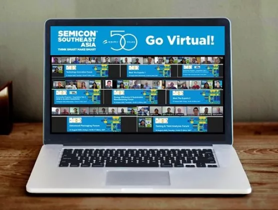
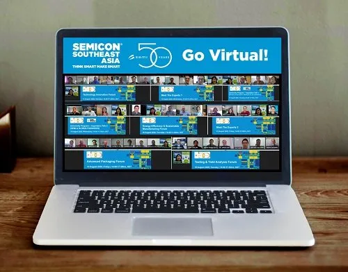
Never before had we expected that SEMICON SEA 2020 would go virtual.The COVID-19 crisis abruptly halted our ability to hold our premier Southeast Asia electronics manufacturing exposition as we typically do – in the physical realm. The pandemic tested our adaptability, challenged our willingness to experiment and, perhaps above all, accelerated not only our own but the world’s digital transformation. We had to change our way of doing business and learn to connect virtually like we had never had before. SEMI continues to believe that virtual interaction is no replacement for face-to-face engagement. But, like the rest of the world, we fast-tracked our digital education and staged the virtual event 20 July to 21 August 2020 to gather supply chain players and help fulfill the tremendous potential of our great industry. For all the suffering the COVID-19 has caused, the pandemic has underscored an important truth – that we need innovation through collaboration now more than ever to help solve the world’s greatest problems. We thank all our event sponsors as we turned what started as a grand experiment into a successful event that drew nearly 3,000 attendees to our webinars, business matching sessions and other online offerings designed to help them uncover new business opportunities. Following are other highlights. Southeast Asia Pavilion at Virtual SEMICON West 2020 In our first collaboration with SEMICON West, our Southeast Asia Pavilion at the event welcomed virtual visitors from around the globe to help them form new connections and grow their businesses. Business Matching Sessions Technical buyers from more than 15 multinational companies along with 141 pre-qualified suppliers attended more than 50 meetings across four online business matching sessions.Technical WebinarsCompany representatives from regions including Malaysia, Singapore, Vietnam, Taiwan, the United States, the UK, Israel, China and Japan shared their expertise and industry insights at SEMICON Southeast Asia 2020 webinars. In addition, experts from leading semiconductor companies such as Micron Semiconductor Asia Operations, ViTrox Corporation Berhad and A*STAR took part in our technical exchange by sharing the latest trends in the rapidly evolving semiconductor industry. Talent Development: Inspirational University Program Talks With building the talent pipeline critical to sustaining growth of Southeast Asia semiconductor manufacturing dynamics, talent champions from Lam Research and GLOBALFOUNDRIES highlighted career opportunities and pathways for young engineers while generating recruiting leads. More than 750 students from Malaysia and Singapore engaged panelists with questions during the sessions. The SEMICON Southeast Asia team extends its tremendous thanks to sponsors and attendees for their support. As we all navigate the pandemic and hope in the near future to awaken to a brighter day, we will continue to connect virtually and, whenever possible, in person as the semiconductor industry evolves and flourishes. The SEMICON SEA 2020 team In the meantime, we will all continue to pull together to support our resilient industry as it outperforms most other manufacturing sectors. Semiconductor capital equipment shipments were up 23% globally in the second quarter of 2020 versus the same period in 2019 and semiconductor chip growth remains in positive territory. Our team has already started planning for SEMICON SEA 2021, scheduled to take place at the Setia Spice Convention Centre in Penang, 18-20 May 2021.We look forward to seeing you again soon as we continue to strengthen the microelectronics ecosystem!Bee Bee Ng is president of SEMI Southeast Asia.
Read More

MILPITAS, Calif. – August 31, 2020 – Staged for the first time in virtual format, MEMS and Sensors Executive Conference (MSEC 2020) will gather industry visionaries and experts October 6-15 for the latest trends and innovations in sensorization for growth markets including medical, entertainment, augmented and virtual reality, the environment, food production, smart cities, ultrasonics and wearables.

MSEC Logo

Themed The Next Wave of Sensorization: Solving our Shared Challenges, the event will focus on solving technology challenges in vital areas such as health and safety while fueling the experience economy with advances in virtual and augmented reality. Components, software, and systems critical to MEMS and sensors innovations will come into sharp focus at the conference. Registration is open.

MSEC Keynotes

Michael Tschanz Photo

Michael Tschanz, Director, Engineering Technology and Analysis

Disney’s extensive use of sensors including for rides, animatronics and sensorization of the world’s largest micro transportation system

Disney Logo
Jens Fabrowsky Photo

Jens Fabrowsky, executive vice president, Automotive Electronics

MEMS market opportunities and technology challenges over the next 10 years

Bosch Logo
Dale Zimmerman Photo

Dale Zimmerman, director for Photonics Devices

MEMS-enabled display for Hololens augmented reality, including applications and market progress

Microsoft Logo

MSEC 2020 will also feature sessions on key industry topics including the following:

  • MedTech Considerations for Resolving the Trouble with Innovative Sensing Applications – Ian Chen, executive director for Medical New Business Development, Maxim Integrated,
  • Opportunities in Biotech and Related Markets Due to COVID-19 –Ross Bundy, co-founder, Cardea
  • MEMS Tug-of-war: COVID-19 vs Emerging Trends – Dimitrios Damianos, technology and market analyst for Imaging and MEMS, Yole Développement,
  • A Wearable Social Distancing Solution Based on Ultrasonic Time-of-Flight Sensors – David Horsley, co-founder, TDK-Chirp Microsystems,
  • tinyML: Massive Opportunity When Machine Intelligence Meets the Real World of Billions of Sensors – Evgeni Gousev, senior director, Qualcomm AI Research
  • AI for Ultrasound Medical Imaging – Janusz Bryzek, executive chairman and CTO, eXo Systems,
  • Future Mobility Enabled by Sensorization – Andreas Breitner, Partner, McKinsey & Company

Premier Sponsors

Event sponsors include Microtech Ventures. 

SEMI MSIG banner

MSEC 2020 is hosted by MEMS & Sensors Industry Group (MSIG), a SEMI technology community. Learn more at Virtual MSEC 2020.


About SEMI
SEMI® connects more than 2,400 member companies and 1.3 million professionals worldwide to advance the technology and business of electronics design and manufacturing. SEMI members are responsible for the innovations in materials, design, equipment, software, devices, and services that enable smarter, faster, more powerful, and more affordable electronic products. Electronic System Design Alliance (ESD Alliance), FlexTech, the Fab Owners Alliance (FOA) and the MEMS & Sensors Industry Group (MSIG) are SEMI Strategic Technology Communities, defined communities within SEMI focused on specific technologies. Visit www.semi.org to learn more, contact one of our worldwide offices, and connect with SEMI on LinkedIn and Twitter.

Association contact

Scott Stevens, Cardinal Communications for SEMI Americas
Phone: 1.512.288.4050
Email: [email protected]

MILPITAS, Calif. – August 24, 2020 – SEMI, the industry association serving the global electronics design and manufacturing supply chain, today released the following statement in response to the new export control rule changes announced by the United States Commerce Department.

SEMI recognizes the role of export control measures to address threats to U.S. national security. However, we are very concerned the new export control regulations issued on August 17, 2020, by the U.S. Department of Commerce will ultimately undermine U.S. national security interests by harming the semiconductor industry in the U.S. and creating substantial uncertainty and disruption in the semiconductor supply chain. On July 14, in public comments on the May 15 regulations, SEMI cautioned that those relatively narrow actions created unique disincentives to purchase U.S.-origin semiconductor equipment and design software and had already resulted in $17 million lost sales of U.S-origin items to firms unrelated to Huawei.

Commerce’s decision to significantly expand these unilateral restrictions will likely lead to more lost sales, eroding the customer base for U.S-origin items. The new restrictions will also fuel a perception that the supply of U.S. technology is unreliable and lead non-U.S. customers to call for the design-out of U.S. technology. Meanwhile, these actions further incentivize efforts to supplant these U.S. technologies.

SEMI respectfully requests Commerce immediately extend to 120 days the savings clause for items in production before August 17, ensure predictable and timely license decisions for all items and significant flexibility for licenses unrelated to 5G items. We also urge the administration to pursue policies with fewer unintended consequences and damage to U.S. technology leadership. Revenue from global sales is a major source of U.S. research and development (R&D) funding in these technologies; lost global revenue will lead to a decrease in R&D, undermining U.S. semiconductor innovation and thereby harming national security.

About SEMI

SEMI® connects more than 2,400 member companies and 1.3 million professionals worldwide to advance the technology and business of electronics design and manufacturing. SEMI members are responsible for the innovations in materials, design, equipment, software, devices, and services that enable smarter, faster, more powerful, and more affordable electronic products. Electronic System Design Alliance (ESD Alliance), FlexTech, the Fab Owners Alliance (FOA) and the MEMS & Sensors Industry Group (MSIG) are SEMI Strategic Technology Communities, defined communities within SEMI focused on specific technologies. Visit www.semi.org to learn more, contact one of our worldwide offices, and connect with SEMI on LinkedIn and Twitter.

SEMI Contact

Samer Bahou/SEMI
Phone: 1.408.943.7870
Email: [email protected]

MILPITAS, Calif. — August 20, 2020 — North America-based manufacturers of semiconductor equipment posted $2.60 billion in billings worldwide in July 2020 (three-month average basis), according to the July Equipment Market Data Subscription (EMDS) Billings Report published today by SEMI. The billings figure is 11.8 percent higher than the final June 2020 level of $2.32 billion, and is 27.6 percent higher than the July 2019 billings level of $2.03 billion.

“The second half of 2020 has started strong with double-digit billings growth for North America-based semiconductor equipment manufacturers,” said Ajit Manocha, SEMI president and CEO. "The strength reflects the semiconductor industry's criticality in today's world and the driving forces in place for long-term industry growth."

The SEMI Billings report uses three-month moving averages of worldwide billings for North American-based semiconductor equipment manufacturers. Billings figures are in millions of U.S. dollars.


Billings
(3-mo. avg.)

Year-Over-Year

February 2020

$2,374.6

27.1%

March 2020

$2,213.1

21.2%

April 2020

$2,281.3

18.7%

May 2020

$2,343.3

13.5%

June 2020 (final)

$2,317.7

14.4%

July 2020 (prelim)

$2,591.9

27.6%

Source: SEMI (www.semi.org), August 2020

SEMI publishes a monthly North American Billings report and issues the Worldwide Semiconductor Equipment Market Statistics (WWSEMS) report in collaboration with the Semiconductor Equipment Association of Japan (SEAJ). The WWSEMS report currently reports billings by 24 equipment segments and by seven end market regions. SEMI also has a long history of tracking semiconductor industry fab investments in detail on a company-by-company and fab-by-fab basis in its World Fab Forecast and SEMI FabView databases. These powerful tools provide access to spending forecasts, capacity ramp, technology transitions, and other information for over 1,000 fabs worldwide. For an overview of available SEMI market data, please visit www.semi.org/en/MarketInfo.

The data contained in this release were compiled by David Powell, Inc., an independent financial services firm, without audit, from data submitted directly by the participants. SEMI and David Powell, Inc. assume no responsibility for the accuracy of the underlying data.

About SEMI

SEMI® connects more than 2,400 member companies and 1.3 million professionals worldwide to advance the technology and business of electronics design and manufacturing. SEMI members are responsible for the innovations in materials, design, equipment, software, devices, and services that enable smarter, faster, more powerful, and more affordable electronic products. Electronic System Design Alliance (ESD Alliance), FlexTech, the Fab Owners Alliance (FOA) and the MEMS & Sensors Industry Group (MSIG) are SEMI Strategic Technology Communities, defined communities within SEMI focused on specific technologies. Visit www.semi.org to learn more, contact one of our worldwide offices, and connect with SEMI on LinkedIn and Twitter.

Association Contact

Michael Hall/SEMI
Phone: 1.408.943.7988
Email: [email protected]

Notes

Next SEMI Billings report is September 17, 2020 at 3:00pm Pacific.
For information on SEAJ Billings Express Report, visit www.seaj.or.jp.


To attract and cultivate new talent across the microelectronics industry, virtual SEMICON West 2020 offered wide-ranging career insights for engineering students seeking that vital first job and young employees embarking on their careers. They learned about overcoming challenges at work and gained a competitive edge by connecting with industry leaders for insider knowledge. These are just some examples of how the SEMI Foundation and the SEMI Workforce Development and Diversity, Equity and Inclusion (DEI) initiatives serve as a springboard to careers in the industry and help close its talent gap.Following are experiences of aspiring engineers at SEMICON West and career lessons presented to help them shape the future of our semiconductor industry.Jump-Starting Careers at SEMICON West 2020More than 600 students from over 50 colleges and universities across the Unites States joined SEMICON West 2020 to jump-start their careers in the semiconductor industry. With free access to SEMI’s first virtual expo, they connected with recruiters and companies in the exhibit hall, and sponged up insights from speakers about digital internships, job opportunities, and key trends shaping the digital future.“It was almost overwhelming,” said Jason Wong, 20, a junior at San Jose State University working toward an advanced degree in mechanical engineering. “It was kind of like an engineering student’s dream for contacts and knowledge all on one platform.”Wong visited about 15 booths in the online exhibit hall to speak with company representatives about his field of interest – microelectromechanical systems (MEMS).“MEMS is a pretty niche area, so it was really surprising how many companies were there in this category alone,” Wong said.Through the expo’s chat tool, Wong made some solid contacts and has followed up with several engineers via email, LinkedIn and Zoom meetings, cultivating what he believes will be “some long-lasting and valuable connections.”“I’m not really looking for a job at the moment, but I hope to get an internship at some point,” Wong said. “With the current (COVID-19) outbreak, a lot of events with opportunities to interact are no longer available, so this was an enlightening and useful experience for me I plan to attend again.”On the other side of the country in Virginia, Devayani Pawar, 23, found it easy to network at SEMICON West. She especially appreciated the free pass for students and practical sessions in the Smart Workforce Pavilion tailored to help early-career job seekers find opportunities, build contacts, and polish resumes.She was drawn to the Smart Manufacturing Pavilion because of her skills and interests in toolmaking and wafers.“I understand manufacturing and it’s a hot field right now,” said Pawar, who recently earned her master’s degree in data science from George Mason University. “It’s interesting to me how such tiny components can do so much powerful work.”“A lot of people my age aren’t very aware of the microchip industry – they’re mostly focused on information technology and companies like Google, Amazon, or Facebook,” Pawar said.After landing an internship at Micron Technology analyzing wafers and working in clean rooms, she was wowed by the potential of nanotechnology. Pawar learned about the strong demand for data scientists in semiconductor manufacturing. After making connections at SEMICON West and absorbing information, she now has a better handle on career opportunities.“The recruiters and other contacts I made have been so responsive, and now I have a better understanding of use cases and what companies are seeking,” she said.A Day in the Life of an EngineerRight after college in 2017, Erika Gabrielle Hansen joined Applied Materials as an engineer. She told management she wanted to travel, learn about the “big picture” behind the company’s products, and work with customers.In her presentation A Day in the Life of an Engineer at the SEMICON West Smart Workforce Pavilion, she recalled a whirlwind of unforeseen opportunities, soul-searching challenges, and the rewards of personal, professional, and community growth. She also candidly shared lessons learned about pride, collaboration, and resilience.Her journey began when she had the opportunity to share her aspirations for her at career at Applied and landed a dual role as a process engineer and customer account technologist.In her job as a process engineer, Hansen puts her materials engineering degree from Cal Poly, San Luis Obispo to good use analyzing data, solving technical problems, developing new processes to meet customer requirements, and working with cutting-edge technologies. At one moment she might be in a clean-room laboratory wearing a bunny suit doing hands-on work with tools. In another, she could be videoconferencing with hardware, software, and systems engineers worldwide, or preparing a report for upper management.“I was very nervous at first as a process engineer,” Hansen said. “I was the only person in my group who didn’t have a Ph.D. and tried to compensate for that by doing things on my own and not asking for help.”After making a few mistakes, she began to turn to her team for their expertise and sharing the results of her work – both good and bad – with them.“Having humility to ask for help and not let pride get in the way was a huge learning point for me,” she said.As a customer account technologist, she has made a dozen trips to customer sites in four countries to implement new processes or resolve technical issues. By seeing tools in action, she now has what she calls a “whole picture” perspective on their effectiveness, while enjoying the camaraderie of colleagues and sampling local cuisines, sites, and scenes around the world.At one point, she was assigned to lead an international team to resolve an issue with a major customer – her greatest challenge yet and her first time in such a role. She struggled to overcome language barriers and eventually told her boss she might not be the best person to lead the project. He promised to provide more support, and her team went on to resolve the customer’s problem.“I picked myself up, reached out to people with international experience, and changed my communication style,” Hansen said. “I learned it’s okay to be uncomfortable, to flex my leadership style, and be resilient, which is a learned skill.”Building a Better Network: Crucial ConnectionsAndrew Carnegie, one of history’s richest industrialists and most generous philanthropists, said 85 percent of a person’s success is based on “interpersonal relationships” and “abilities to be a human being.” Professional skills account for just 15 percent of success.While advancing to her current role as Chief Marketing Officer for FormFactor, Amy Leong found this advice critical to her career trajectory. Just like the challenge of raising a strong family, building a successful career “takes a village… you can’t do it alone,” she said in her Smart Workforce Pavilion presentation Building a Better Network: Crucial Connections.Outperforming expectations might be essential early in one’s career to get promotions, raises, and the attention, but that mindset goes only so far.“As seniority levels increase, people already know you’re a phenomenal performer and expect nothing less,” Leong said. “So, the higher you go the more vital it is to spend almost a disproportionate amount of effort on building relationships.”Building your network isn’t about the quantity of one’s business cards or LinkedIn connections; it’s about building quality relationships with mutual benefits over the long run.“We need to be smart about return on investment when building our professional network,” she said. “You help me, and I help you. It’s win-win horse trading.”And the most important factor in career success? For Leong, a strong family foundation has mattered most.“Family comes first,” said Leong, who has twin teenagers. “Take care of the ones you love. Check in with your family whenever you can. Family relationships are bound by blood. Thanks to my retired parents and a helpful husband, we tough it through.”She reemphasized the importance of mutually beneficial relationships, noting “A rising tide will lift all boats.”Fostering Talent for the Industry’s FutureDeveloping young talent and future leaders in microelectronics stands as a persistent and growing need – and a critical challenge to realizing expected growth. Emerging technologies such as artificial intelligence, quantum computing, and augmented/virtual reality are expected to impact a huge range of markets, leading to projections that the semiconductor industry will double in size in the next 10 to 15 years.The opportunities for growth and technologies that promise to improve the quality of human life worldwide are breathtaking. The industry’s talent pool will need to scale accordingly, magnifying the importance of expanding industry-wide programs such as the Workforce Development and DEI initiatives that the SEMI Foundation are building. Learn more about how you and your company can get involved with these initiatives on the SEMI Foundation website.Shari Liss is executive director of the SEMI Foundation. She oversees SEMI Workforce Development programs from K-12 through re-skilling for veterans.
Read More

HSINCHU, Taiwan – August 18, 2020 –SEMI today announced the formation of a new standards committee that aims to develop global standards for flexible hybrid electronics (FHE) spanning design, materials, manufacturing, packaging and systems and to drive industry growth. Unanimously endorsed by members of the SEMI North America Regional Standards Committee (NARSC) and approved by the SEMI International Standards Committee (ISC), the technical committee is the world’s first to focus on flexible hybrid electronics standards. The SEMI Standards Flexible Hybrid Electronics Global Technical Committee has established its first chapter in Taiwan.
semi logo

“The SEMI Standards Flexible Hybrid Electronics Global Technical Committee sets out to clear development bottlenecks facing the industry and establish unified measurement standards for flexible smart textile, automotive, Internet of Things (IoT) and related devices,” saidTerry Tsao, SEMI Chief Marketing Officer and president of SEMI Taiwan. “The Taiwan chapter looks forward to kicking off the development of international industry standards that help Taiwan's FHE sector promote industry growth by reducing costs and increasing competition.”

Initial work of the SEMI Standards Flexible Hybrid Electronics Global Technical Committeewill include establishing working groups to draft measurement standards; building industry consensus on the need for materials, equipment and manufacturing standards; and developing standards to accelerate the introduction of related FHE technologies into diverse consumer end markets.

“We are very pleased to see the establishment of the SEMI Standards Flexible Hybrid Electronics Global Technical Committee and are proud to be part of the working committee to draft the standards,” said Steve Huang, executive director of Taipei-based AiQ Smart Clothing, an innovator with a significant pool of smart textile IP. “As a pioneer in smart textile applications, we are keenly aware of the challenges posed by an absence of standards and how it stifles mass adoption of new technologies.”

The SEMI International Standards Program is in its 47th year, with the 1,000th SEMI Standard published last year. SEMI Standards cover fields including semiconductors, displays, photovoltaics, microelectromechanical systems (MEMS) and smart manufacturing.

For more information, visit the SEMI Standards web page.

About SEMI

SEMI® connects more than 2,400 member companies and 1.3 million professionals worldwide to advance the technology and business of electronics design and manufacturing. SEMI members are responsible for the innovations in materials, design, equipment, software, devices, and services that enable smarter, faster, more powerful, and more affordable electronic products. Electronic System Design Alliance (ESD Alliance), FlexTech, the Fab Owners Alliance (FOA) and the MEMS & Sensors Industry Group (MSIG) are SEMI Strategic Technology Communities, defined communities within SEMI focused on specific technologies. Visit www.semi.org to learn more, contact one of our worldwide offices, and connect with SEMI on LinkedIn and Twitter.

Association Contact

Irene Huang/SEMI Taiwan
Phone: 886.03.560.1777, ext. 205
Email: [email protected]
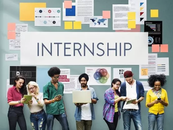
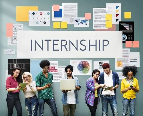
Internships provide a wealth of benefits for students and corporate managers as they work side-by-side in a real-world environment. Students gain practical, hands-on experience and employers get an infusion of fresh energy, diverse ideas and eager talent.The full value of an on-site internship – the ultimate job interview – flowers when it leads to full-time employment.That was before “everything went crazy,” said Tina Revels, university relations manager at KLA, during her Smart Workforce Pavilion presentation The New Reality: Digital Internships at the virtual SEMICON West 2020. Today, amid COVID-19 restrictions, everyone must adjust to a new reality – a virtual reality. Part of this substantial shift has led to internships going digital.“Internships are more important than ever as we shift to a virtual reality,” Revels said, explaining how today’s job seekers and companies alike can make sure digital internships sustain the same mutual benefits as traditional ones.At companies turning to digital internships, managers need to do more upfront planning to re-create real-world experiences that make interns “feel engaged and connected with one another,” Revels said. For prospective interns, digital internships require greater independence, self-management discipline, and responsibility than traditional internships – all critical skills that can lead to permanent employment.Watch Revels’ full presentation below to learn how to get the most out of digital internships. Register for virtual SEMICON West 2020 to access the additional Smart Workforce and Diversity, Equity and Inclusion sessions, which covered dynamic topics such as job searches during uncertain times, creating a culture of inclusivity, supplier diversity, and hiring military veterans. The content is available until September 20, 2020.Learn more about the SEMI Foundation and how its Workforce Development and Diversity, Equity and Inclusion initiatives are helping build the electronics manufacturing and design supply chain’s talent pipeline.Bryson Gauff is program manager for SEMI High Tech U.
Read More

MILPITAS, Calif.– August 11, 2020 – SEMI, the industry association serving the global electronics design and manufacturing supply chain, today launched a new collaborative apprenticeship program to make it easier for companies to offer training and for more workers to pursue careers in electronics. The competency-based SEMI Industry Approved Apprenticeship Program (IAAP) is designed to identify skills gaps and deliver targeted training that efficiently meets industry employers’ hiring needs.

semi logo

SEMI developed the IAAP in partnership with GLOBALFOUNDRIES® (GF®), the largest pure-play semiconductor foundry in the U.S. and the world’s leading specialty foundry. Designed to be scaled to meet industry demand for technicians, the program leverages SEMI’s Unified Competency Model (UCM), which was formed with industry input as a new skills standard and is endorsed by the U.S. Department of Labor Employment and Training Administration (USDOL-ETA). The UCM is posted on DOL-ETA’s Competency Model Clearinghouse.

“GLOBALFOUNDRIES has long been committed to building educational partnerships that benefit both our employees and the region, particularly in developing a highly skilled workforce to ensure our industry and the U.S. remains at the forefront of innovation for years to come," said Ron Sampson, senior vice president and general manager of U.S. Fab Operations at GF. “Through SEMI’s new Industry Approved Apprenticeship Program, we look forward to helping our employees advance their careers, while playing an important role in workforce training and boosting the semiconductor manufacturing talent pool."

“The IAAP is designed to help the microelectronics industry and advanced manufacturers overcome the talent shortage by enabling companies to fill skills gaps more effectively and at lower cost,” said Mike Russo, vice president of Industry Advancement and Government Programs at SEMI. “SEMI will continue to work to ensure the IAAP lays a path for employers to pursue government-registered apprenticeship programs and qualify for reimbursement of related training expenses.”

Hudson Valley Community College (HVCC) will offer the apprenticeship program courses, the first certified under the SEMI Certs program, online.  The course curriculum is aligned with UCM to ensure course curriculum supports the development of skills required by the electronics industry. 

“We are excited to be a partner in this pilot program that is expected to graduate approximately 50 apprentices by the end of this year and more than 100 apprentices by the end of 2021,” said Roger Ramsammy, president of Hudson Valley Community College. “Hudson Valley’s participation in the SEMI Certs program has ensured our courses are aligned with industry requirements and that participants receive college credits to help them pursue related degrees and support career laddering. In addition, we hope the program will ultimately be a New York State Registered Apprenticeship Program, providing access to tuition reimbursement for Required Technical Training.”

Along with GLOBALFOUNDRIES and HVCC, SEMI partnered with SUNY Polytechnic Institute, the Manufacturing Association of Central New York (MACNY) and the Center for Economic Growth (CEG), a nonprofit economic and business development organization that serves as the primary point of contact for businesses interested in growing in or moving to New York’s eight-county capital region, to develop the apprenticeship program. 

The apprentice program marks a milestone in the evolution of SEMI Works™, the first U.S. electronics workforce development program developed under a partnership with the National Science Foundation Advanced Technological Education (NSF-ATE) Program, the USDOL-ETA  and academic partner SUNY Polytechnic Institute in New York. 

About SEMI

SEMI® connects more than 2,400 member companies and 1.3 million professionals worldwide to advance the technology and business of electronics design and manufacturing. SEMI members are responsible for the innovations in materials, design, equipment, software, devices, and services that enable smarter, faster, more powerful, and more affordable electronic products. Electronic System Design Alliance (ESD Alliance), FlexTech, the Fab Owners Alliance (FOA) and the MEMS & Sensors Industry Group (MSIG) are SEMI Strategic Technology Communities, defined communities within SEMI focused on specific technologies. Visit www.semi.org to learn more, contact one of our worldwide offices, and connect with SEMI on LinkedIn and Twitter.

SEMI Contact
Michael Hall/SEMI
Phone: 1.408.943.7988
Email: [email protected]
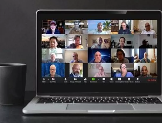
Tracking and quickly diagnosing COVID-19 infections, working from home and telemedicine recently came into sharp focus as technology executives and other subject matter experts from microelectronics heavyweights recently gathered for the first-ever virtual SEMI CTO Forum to explore how the microelectronics industry and their own companies can leverage future technology trends to drive growth. Themed Intelligent Medtech and Wearable Technologies, the forum drew CTOs from ARM, Babblelabs, Brewer Science, Dell, Dow/Dupont, E-Ink, Hewlett Packard Enterprise, Intel, Lam Research, KLA, Microchip, ON Semiconductor, Qualcomm, Tokyo Electron, Ulvac, Veeco and Xilinx. The event is designed as a strategic driver of pre-competitive innovation. Following are key takeaways from the forum. Microfluidics Promises to Speed COVID-19 Diagnosis More than 240 companies worldwide are developing microfluidics solutions to improve diagnosis and treatment of COVID-19 and other conditions, said forum speaker Dr. Kurt Petersen, a member of Band of Angels, Silicon Valley's oldest angel investment group, with an illustrious background1 in technology. And their innovations are bearing fruit. Cepheid, a company founded by Dr. Petersen, has developed a disposable microfluidic cartridge, Xpert Xpress SARS-CoV-2, used by doctors to swab the inside of a patient’s mouth. Highlighting the vital role of MEMS in medical electronics, the tiny powerful devices are behind a test that can detect COVID-19 infection in under 40 minutes. Dr. Petersen also cited a few examples of implantables and injectables under development, including: In vivo chemical sensing: Profusa developed a continuous glucose monitoring sensor via an optical patch. Glaucoma pressure monitors: Injectsense built a silicon chip the size of a grain of rice that is embedded in the eye to measure eye pressure. Retinal implants: Second Sight implanted a 60-electrode array chip that projects images onto the retina to improve vision. Microelectronics Takes Aim at Battling COVID-19 The event’s CTO roundtable, a platform for discussing societal and technology issues, revealed microelectronics technology will likely give rise to solutions for combatting pandemics and new business opportunities both in the short and long run. Areas of the greatest interest included: Tracking and Security: Infection tracking accuracy is key to limiting the spread of viruses yet comes with inherent privacy and security challenges. The consensus view of the executives was that developing trusted hardware capabilities is critical for adoption of accurate infection-tracking technologies. Remote Operation: Executives expect working from home or the use of telehealth to continue building momentum long after pandemic. To give staying power to the remote communications at the heart of these trends, microelectronics ecosystems will need to boost compute performance, both at the edge and in the cloud, while increasing bandwidth to enable applications such as augmented reality/virtual reality (AR/VR), artificial intelligence (AI), machine learning and advanced data analytics. Edge intelligence: The challenge of remote communications spans both people and the Internet of Things (IoT). Questions persist about how hundreds of billions of sensors will connect to the cloud and how much power they will consume. The need to push computing to where data is generated – at the edge – is rising and the necessary underlying technologies will only come by combining various forms of distributed computing and analytics. The microelectronics industry’s ability to seize these opportunities will only be possible with huge strides in innovation, raising concerns among the CTOs about the financial viability of cutting-edge devices because of increasing device complexity and R D costs. Technology partnerships and collaborations – an area where SEMI is contributing and will continue to expand its efforts as it works with the CTO community – will be critical to containing R D costs. SEMI will help the executives identify and mobilize the resources key to future innovation. Improving Home, Work Productivity and Experiences Key to AR Adoption Smart wearables also offer great promise. In just over a decade, AR and VR have grown from science fiction to practical uses such as AR applications for smart contact lenses, said Dr. Mike Wiemer, Co-Founder and CTO of Mojo Vision2. Dr. Wiemer said that while many AR applications remain under development, the technology will only see widespread adoption once it starts to improve productivity and efficiency at home and work and the quality of other experiences. The smart augmented reality contact lens developed by Mojo Vision is a step in that direction. The product’s built-in display gives users timely information about everything they see while remaining invisible by packing 70,000 pixels into a space smaller than a half a millimeter across, making it the smallest and densest dynamic display ever made. The contact lens is powered by an ARM-based processor, with later versions adding an image sensor, eye-tracking sensors and a communications chip. SEMI thanks EMD Performance Materials and Telit for sponsoring the CTO Forum. For more information on the CTO Forum and SEMI’s Smart Data-AI initiative, please sign up on our webpage. 1 Dr. Kurt Petersen is a member of the National Academy of Engineering, an IEEE Medal of Honor winner, and a Life Fellow of the IEEE for his contributions to the commercialization of MEMS technology. 2 Dr. Wiemer also co-founded Solar Junction, where he led technical teams to two world records in solar cell efficiency (43.5% and 44%). He also has patents and papers in Semiconductor Devices Applications, Silicon Photonics, Materials Integration, Lasers, Solar Cells, Solar Systems, and Analog Circuits. Tom Salmon is Vice President of Collaborative Technology Platforms at SEMI. Pushkar P. Apte, Ph.D., is Strategic Technology Advisor for the Smart Data AI Initiative at SEMI.
Read More

MILPITAS, Calif. – August 5, 2020 – With advanced materials a critical enabler of semiconductor growth applications, the stage is set for Strategic Materials Conference (SMC 2020), the premier event offering the latest market insights into drivers of advanced materials in the microelectronics supply chain. A virtual event September 29-October 1, 2020, SMC will highlight opportunities and demand for key enabling materials across the electronics supply chain. SMC registration is now open.

Themed Leading Future Technology Innovations with Materials, SMC will gather top executives and leaders from every segment of semiconductor manufacturing to provide the latest developments in advanced materials including:

  • Economic, Geopolitical and Market Trends
  • Materials Innovation Market Drivers
  • Emerging Materials and Applications
  • Metrology Innovations
  • Advanced Packaging Materials Integration and Challenges
  • Innovative Startup Companies and Venture Capital Investors (New Panel Session)

SMC 2020 Keynotes

Sean Ding, Alibaba

Sean Ding, Chief Technology Officer of IoT
Digitizing the Physical World Enables Digital Transformation

Alibaba
Jun He, TSMC

Jun He, PhD, Head of Corporate Quality and Reliability
A New Era of Supply Chain Collaboration: Driving Socially Responsible Semiconductor

tsmc
Anand Nambiar, Merck

Anand Nambiar, Global Head, Semiconductor Materials
How the Next Decade of Materials Innovation Will Advance Digital Living 

MERCK
John Smythe, PhD

John Smythe, PhD, Advanced Technology Lead DMTS
The Power and Limitations of Materials Solutions

Micron logo

Industry leaders presenting at SMC 2020 include:

  • Alibaba Group
  • AT&S
  • Applied Ventures
  • Ayar Labs
  • BCA Research
  • Carbon
  • El Camino Capital
  • Hilltop Economics
  • IBM TJ Watson Research Center
  • Intel Capital
  • Intel Corporation
  • JSR Micro
  • Kebotix
  • KLA
  • Lyncean Technologies
  • Marvell Semiconductor
  • Onto Innovation
  • OTI Lumionics
  • Samsung Ventures
  • Stanford University
  • TEL
  • TSMC
  • VLSI Research
  • Xilinx

About SEMI

SEMI® connects more than 2,400 member companies and 1.3 million professionals worldwide to advance the technology and business of electronics design and manufacturing. SEMI members are responsible for the innovations in materials, design, equipment, software, devices, and services that enable smarter, faster, more powerful, and more affordable electronic products. Electronic System Design Alliance (ESD Alliance), FlexTech, the Fab Owners Alliance (FOA) and the MEMS & Sensors Industry Group (MSIG) are SEMI Strategic Technology Communities, defined communities within SEMI focused on specific technologies. Visit www.semi.org to learn more, contact one of our worldwide offices, and connect with SEMI on LinkedIn and Twitter.

Association Contacts

Michael Hall/SEMI
Phone: 1.408.943.7988
Email: [email protected]
Scott Stevens, Cardinal Communications for SEMI Americas
Phone: 1.512.288.4050
Email: [email protected]