downloadGroupGroupnoun_press release_995423_000000 copyGroupnoun_Feed_96767_000000Group 19noun_pictures_1817522_000000Member company iconResource item iconStore item iconGroup 19Group 19noun_Photo_2085192_000000 Copynoun_presentation_2096081_000000Group 19Group Copy 7noun_webinar_692730_000000Path
Skip to main content
Default Banner Image

China

Back in 2012, China ranked fifth among seven regions worldwide in IC wafer capacity but surged past the Americas and Japan in 2018 and 2019 to claim the number three position (figure 1). That’s a big deal given that ICs account for the largest share of wafer capacity excluding discrete, opto, MEMS and sensors.China’s IC wafer capacity growth accelerated to tune of 14% in 2019 and 21% in 2020 and is expected to grow at least 17% this year, as we report in the latest update of the World Fab Forecast, published December 3rd by SEMI. Of all regions, Taiwan boasts the second strongest growth rate over the same period at 3% to 4%.Figure 1: Total IC installed wafer capacity for top five regions The report shows that from 2019 through the end of 2021 China will have increased wafer capacity for memory by 95%, foundry by 47% and analog by 29%. Foundry will represent the largest portion of those gains, reaching 2 million wpm (200mm equivalents). Memory will follow at about 1.5 million wpm and then analog at over 120,000 wpm.But Chinese companies aren’t pulling off this feat singlehandedly. Many international companies are contributing to the wafer capacity increases in China (figure 2). Figure 2: IC wafer capacity in China by company origin The share of capacity contributed by Chinese-owned companies and international companies has changed little since 2012, though Chinese-owned companies saw a slight dip in their slice of the pie from 60% to 57%From 2019 through 2021, Chinese-owned companies will add almost 60% capacity for foundries, the most of all sectors. Companies including SMIC, Hua Hong Semiconductor, Nexchip, XMC and Hua Li Microelectronics are driving the increases.During the same period, Chinese-owned companies will ramp up memory capacity from basically zero to 300,000 wpm. Companies such as Yangtze Memory Technology and ChangXin Memory Technologies (CXMT), also known as Innotron, are powering the quick rise with aggressive ramps of 3D NAND and DRAM capacity.Among international-owned companies, TSMC and UMC are driving the largest share of foundry growth, while Samsung, SK Hynix and Intel are powering gains in memory capacity.More information is available in the World Fab Forecast report. The report currently collects information for fab equipment and construction investment, capacities, technologies and product types for over 280 fabs and lines in China alone, including 40 facilities that either began operation in 2020 or will from 2021 through 2024.Christian G. Dieseldorff is senior principal analyst in the Industry Research and Analysis group at SEMI in Milpitas, California.
Read More
If you think the world is flooded with a mind-boggling volume of digital content, then you might be just a amazed to learn about the sheer wealth of information and business opportunities that will be uncovered at this year’s SEMICON Japan as the event goes full digital.To start, more than 160 companies will exhibit their semiconductor manufacturing gear and services on the virtual show floor of Japan’s premier event for the semiconductor manufacturing and design supply chain. Add to that over 80 presentations and panels that feature global industry executives, visionaries and experts offering insights into the latest microelectronics developments, trends and technologies, and it’s easy to see how SEMICON Japan 2020 Virtual is designed to help attendees grow their businesses and the industry drive the next wave of innovations that promise to address some of the world’s greatest challenges across healthcare, the environment, transportation and other industries.Best of all, it will all be available at your convenience from your office or home 24 hours a day, making it safe and easy for you and others from all over the world to attend. Following is what’s in store at SEMICON Japan 2020 Virtual to help lead you into the future.Leading Japanese Securities Analysts to Weigh in What’s Ahead for the Chip Equipment Sector in 2021 For the first time, SEMICON Japan will feature Bulls Bears as Japan’s’ five top securities analysts focus on the 2021 outlook for the global semiconductor equipment sector. The December 17th event will include discussions on the COVID-19 pandemic’s impact on the semiconductor industry, the continuing geopolitical tensions that are forcing the industry to reconfigure its supply chains, the fast-growing China market and cutting-edge applications that are powering industry growth. The perspectives from Japan’s investment community are sure to be compelling as the region supplies one-third of the global semiconductor industry’s chip manufacturing equipment.Moderated by Akira Minamikawa of OMDIA, the panel will include these experts:Three Visionaries to Explore the Digital TransformationPowered by semiconductors, the fourth industrial revolution is driving digitalization globally, remaking societies to bring more efficiencies and conveniences to our work and home lives and help more people prosper. But the flip side of those tremendous benefits is the risk that wealth will be concentrated in the hands of people in positions of power, companies and nations. Democratizing economic development remains a serious challenge worldwide.Addressing this pressing issue, the Opening Panel on December 11 will feature prominent visionaries from political, academic and industrial communities including the following:Sony’s Leading-Edge Electric Car and Nissan’s Driver Assistance System to Highlight Automotive InnovationsCars are becoming more like smartphones on wheels, rapidly filling with more and more semiconductor chips every year with electrification and electronic driver-assisted systems to key drivers of this growth. At the SMART Mobility 1 session on December 14, two pioneering companies – Sony and Nissan Motor – will focus on both areas of semiconductor innovation.Sony’s Vision-S concept car, exhibited at CES 2020, astonished many in the electronics ecosystem and the automotive industry. What is Sony’s vision behind the vehicle? Izumi Kawanishi, Senior Vice President, AI Robotics Business at Sony will share the latest on the initiative.Nissan, maker of the pioneering LEAF electric vehicle, is the first Japanese carmaker to equip a car – its new Skyline – with the ProPILOT 2.0 driver assistance system for hands-off highway driving. Nissan Executive Vice President Asako Hoshino will provide an update on the company’s driver assistance system strategy and plans.Quantum Computing Meets Chip Manufacturing for the First Time at SEMICON Japan In contrast with current computer systems that use bits (binary 0 or 1 state) for computing, quantum computers leverage quantum superposition (0 and 1 states exist at once) to quickly solve highly complex problems that might take traditional supercomputers hundreds or even thousands of years to tease out. American physicist Richard Feynman promoted quantum computer as early as 1982, but it wasn’t until nearly two decades later and long after his death that quantum bit circuits emerged for use in superconductive materials.With quantum circuits and devices requiring state-of-art semiconductor processing technology, The Era of Quantum session on December 15 at SEMICON Japan 2020 Virtual will discuss necessary advances in chip manufacturing technology to enable the next generation quantum computing. The session will be the first time SEMICON Japan connects the semiconductor manufacturing and quantum computing communities.The program will feature the following experts:Strategies for Sustainable Semiconductor Industry GrowthSemiconductors are giving rise to a hyper-connected world that is fueling demand for staggering volumes of chips, pressuring the electronics industry to uncover new ways to increase manufacturing efficiency while reducing power consumption in a bid to help combat climate change. The Grand Finale Panel composed of executives from Japan’s semiconductor supply chain and a supervising ministry will gather for the Grand Finale Panel on December 18 to discuss ways the industry can achieve sustainable growth through innovation with a focus on energy savings and an new process technologies such as extreme ultraviolet lithography (EUV), which promises to enable electronics devices that are more power powerful, cheaper and more energy-efficient.Panelists include the following:Register TodayThe SEMICON Japan 2020 Virtual All-In Pass provides online access to all 80 presentations and panels, which will be available on-demand for replay until January 15, 2021. What’s more, all eight keynote programs will feature English subtitles. For complete information of the exposition, programs and registration, visit the SEMICON Japan website.I look forward to seeing you virtually at the event!Jim Hamajima is president of SEMI Japan.
Read More
The global economy has started down a gradual path to recovery from COVID-19 in recent months as the world continues to combat the virus. Yet one sector – semiconductors – has shown impressive growth powered by a transformation hastened by the pandemic across industries ranging from education and work-from-home to healthcare.Semiconductor sales increased 12% in September to mark a second consecutive month of double-digit growth, and year-to-date semiconductor receipts as of September jumped 5.5% compared to the same period in 2019, according to SIA/WSTS.While this upward trajectory is encouraging, it pales compared to 2020 semiconductor equipment billings growth, with results from SEMI showing worldwide global chip equipment billings in September soaring to a new high of $7.6 billion this year. During the first nine months of 2020, aggregate equipment billings logged a 23.6% rise compared to the same stretch in 2019, surpassing $51 billion. Better still, the total semiconductor equipment market in 2020 is on track to beat the previous high of $64.5 billion set in 2018.Investments in China, Taiwan and Korea are fueling the chipmaking equipment spending surge. With big domestic and international fab projects in the works, China this year is projected to become the world’s largest capital equipment market for the first time, surpassing Taiwan, which will follow at a close second. Korea will rank third in equipment investments. Taiwan and Korea growth will come on the strength of equipment spending for manufacturing leading-edge semiconductors.Equipment billings in North America and Europe declined year-over-year as the automotive and industrial sectors suffered the heaviest blows from COVID-19. Investment momentum in both regions is expected to pick up in 2021 after automotive production recovers to pre-pandemic levels while factory automation will boost industrial demand.For more information about monthly equipment billing trends by region and equipment segment, please see the SEMI Equipment Market Data Subscription.Clark Tseng is director of Industry Research and Statistics at SEMI.
Read More
As the United States government has expanded semiconductor-related export controls, companies in the global electronics manufacturing and design supply chain have had to spend considerable time and effort navigating restrictions and managing significant new uncertainties emanating from recent policies. On November 9, SEMI submitted comments to the Department of Commerce’s Bureau of Industry and Security (BIS) urging the agency to proceed cautiously and adopt regulatory best practices and microelectronics industry recommendations to ensure that its identification of foundational technologies does not restrain U.S. innovation and exports without furthering essential U.S. national security interests. The comments specifically respond to the August 27 Advance Notice of Proposed Rulemaking (ANPRM), Identification and Review of Controls for Certain Foundational Technologies. The Export Control Reform Act (ECRA) of 2018 required BIS identify certain emerging and foundational technology that is “essential” to U.S. national security and requires such technology to be controlled to China and other nations subject to a U.S. arms embargo. Congress did not provide a specific definition for emerging or foundational technology, nor the term essential, further complicating the process to identify such technology.BIS has already implemented or proposed several emerging technology controls and the ANPRM starts the process to identify potential foundational technology controls. The SEMI comments focus on the fundamental question of how to define foundational technology, and are organized into three main sections: Requirements of ECRA Guidance from ECRA Regulatory best practices and industry recommendations Applying the statutory requirements and guidance, together with best practices and recommendations, to the identification of foundational technology indicates that most semiconductor-related technology, particularly semiconductor manufacturing equipment and materials, should be outside the bounds of the foundational technology initiative. In general, most technology related to semiconductor devices, manufacturing equipment, materials and design software is not essential to U.S. national security and, in cases where such technology does present material national security issues, it is generally subject to the U.S. list review process and multilateral controls. This technology is widely available outside the United States and due to substantial foreign availability, unilateral U.S. controls on such technology are likely to be ineffective in limiting its proliferation and harm U.S. development of or threaten U.S. leadership in this technology.While the SEMI comments focus on the effort to identify foundational technology, the recommendations and best practices apply in all export control contexts. Several of the statements pertain to policy in ECRA, including its imposition of controls to further specific essential U.S. national security interests only after full consideration of their impact on the economy.Other statements derive from factors ECRA requires BIS to consider, such as not seeking to control technology that’s already available outside the U.S. and not imposing controls that would harm U.S. technological development or leadership. An additional key factor is not imposing controls before multilateral controls are agreed to, nor when it is unlikely the relevant multilateral regimes will adopt similar controls, as is likely for technology that has been decontrolled by a regime.Finally, regulatory best practices suggest that technology-based controls should not be imposed when more targeted end-use or end-user controls can address national security concerns and duplicative controls in addition to recent, significant expansions of existing controls are unnecessary.SEMI is pleased to work with the U.S. Department of Commerce and other regulatory agencies, providing industry data, trends and perspectives to ensure export controls effectively serve national security interests without undue harm to technological development and leadership in this dynamic, globally competitive industry.Ways to Stay Connected and Learn MoreSEMI is committed to serving the global electronics manufacturing and design supply chain and present the collective voice of members to governments worldwide.The SEMI Global Update weekly newsletter provides updates on advocacy issues and technology trends and is available to all.Additionally, SEMI hosts live and virtual events that offer analysis and insights of geopolitical trends by industry experts, with the next opportunity to participate coming on December 3 with the SEMI CEO Webinar: Analyzing the Impact of the U.S. Election on the Microelectronics Industry.Joe Pasetti is Vice President of Global Public Policy and Advocacy at SEMI.
Read More
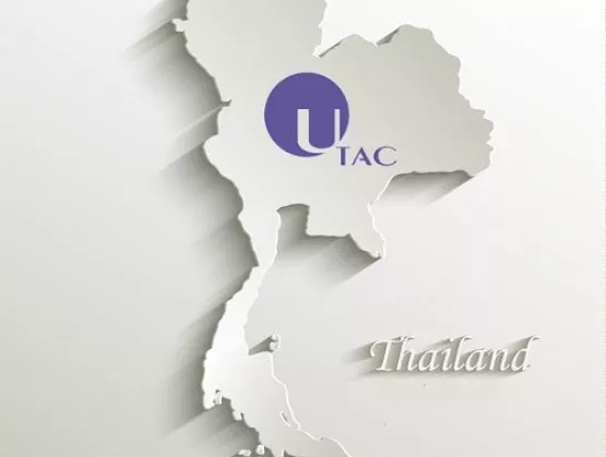
SEMI is pleased to welcome Singapore-based UTAC Holdings Ltd., formed nearly 50 years ago, as a new member. UTAC is a leading independent provider of assembly and test services for a broad range of semiconductor chips, offering a full range of semiconductor assembly and test services across analog, mixed-signal and logic, and memory. Its customers are primarily fabless companies, integrated device manufacturers and wafer foundries. The company has production facilities in Singapore, Thailand, China, Indonesia and Malaysia as well as sales offices in five regions: the United States, Japan, China, Taiwan, the rest of Asia and Europe.I recently spoke with Dr. Nathapong Suthiwongsunthorn, Vice President and General Manager of UTAC Thailand, about UTAC’s smart manufacturing advances, the company’s role in the semiconductor industry’s transformation, and the industry outlook for Thailand over the next year.Ng: How does UTAC Thailand complement your other facilities?Dr. Nathapong: As one of the world’s largest producers of quad-flat-no-leads (QFN), UTAC Thailand has significant capability in assembly and test of advanced leadframe products including power products such as Cu Clip packages as well as MEMS products. We also serve top global IDMs and have the largest share of assembly and test for the automotive market among all UTAC operations. UTAC’s other facilities have expertise in wafer-level packages and system-in-a-package and serves the communication and consumer market not only for IDMs but also for the fabless and foundry companies. The Thailand factory nicely complements the other UTAC facilities both from the standpoint of operational and marketing diversity. Ng: UTAC Holdings Ltd. announced in August this year that it has completed its sale to Wise Road Capital, a global private equity firm. Will this in any way change the operation and business strategy of UTAC Thailand?Dr. Nathapong: I don’t believe it will change the way we operate. However, the acquisition is very positive for us from a financial perspective. With the benefit of significantly reduced debt and interest expenses, we will be able to expand our business to grow with and hopefully beyond the semiconductor market. Ng: To what extent has UTAC adopted smart manufacturing?Dr. Nathapong: UTAC Thailand is leading the way in terms of automation, smart manufacturing and Industry 4.0 with our in-house automation team and unique expertise. For example, we have built our own inspection equipment that is much faster and cheaper than what is commercially available. We also working on many programs such as mobile robot, AGV, auto inspection and office automation to help drive greater production efficiency. We are replicating our manufacturing advances and fanning them out to other UTAC facilities.UTAC Thailand Ng: What are some of the challenges you face in pushing for the industrial transformation in Thailand?Dr. Nathapong: I think the key challenge is to find skilled engineers who can perform hardware- and software-related tasks critical to the industrial transformation. But frankly, we have done a good job in managing this challenge by hiring very smart people, providing them with the required in-house training, and using outside training for new recruits as necessary. We have developed partnerships with capable vendors in this regard as well.Ng: What are the key differentiating elements (e.g. talent, tax, technology, trade, EHS) in Thailand that have been instrumental in supporting the E E ecosystem?Dr. Nathapong: There are two key differentiating elements for us. Firstly, UTAC has been around for over 47 years and is very well-established in Thailand with a positive reputation as an employer. This makes hiring talented people relatively easy. Secondly, and perhaps more importantly, the nature of the Thai people and also the benefits the company provides make it relatively painless to retain key employees. I also believe that we have a significant number of engineers available in Thailand. Finally, labour costs in Thailand are still very reasonable and stable. So we are able to acquire talent at a very competitive rate compared to other countries. Ng: What is the industry outlook for E E industry in Thailand over the next year?Dr. Nathapong: Surprisingly, the current sad predicament of COVID-19 has shown no negative impact for the global semiconductor industry – people seem to be buying more electronics with the lockdown. Our outlook for the Thailand’s E E industry is similarly very positive. Most semiconductor companies including UTAC see significant growth this year and I hope it will continue.Ng: With the recent semiconductor geopolitical and trade tensions, are more customers moving their business to Thailand?Dr. Nathapong: I believe so. We do see some of our key customers move manufacturing out of China and into Thailand. The relocations help them offset or avoid any potential fallout from current geopolitical tensions.Ng: In what areas do you think SEMI Southeast Asia can play a role to help our members companies in Thailand like UTAC?Dr. Nathapong: The semiconductor industry has been in Thailand for a long time. In fact, UTAC Thailand is 47 years old this year! However, I feel that Thailand never really worked with a strong establishment organization like SEMI that can connect various companies together to help drive innovation. I think SEMI Southeast Asia can truly help Thailand to move up to the next level of providing semiconductor solutions globally. We welcome SEMI Southeast Asia’s help in this regard.About Dr. Nathapong SuthiwongsunthornDr. Nathapong Suthiwongsunthorn joined UTAC in 2009 and is currently General Manager of UTAC Thailand, UTAC’s largest operation site. Before taking over the management of Thailand operations, he was Vice President of Research and Development, running UTAC’s global R D group. Dr. Nathapong has more than 20 years of experience in the semiconductor industry. He holds more than 40 international patents and publications in wafer-level and advanced packaging.Prior to joining UTAC, Dr. Nathapong held several key leadership positions in research and development at Schott, STATS ChipPAC and Infineon. Dr. Nathapong has a Ph.D. in Electronics Engineering from Oxford Brookes University, England.Bee Bee Ng is president of SEMI Southeast Asia.
Read More
Never before had we expected that SEMICON SEA 2020 would go virtual.The COVID-19 crisis abruptly halted our ability to hold our premier Southeast Asia electronics manufacturing exposition as we typically do – in the physical realm. The pandemic tested our adaptability, challenged our willingness to experiment and, perhaps above all, accelerated not only our own but the world’s digital transformation. We had to change our way of doing business and learn to connect virtually like we had never had before. SEMI continues to believe that virtual interaction is no replacement for face-to-face engagement. But, like the rest of the world, we fast-tracked our digital education and staged the virtual event 20 July to 21 August 2020 to gather supply chain players and help fulfill the tremendous potential of our great industry. For all the suffering the COVID-19 has caused, the pandemic has underscored an important truth – that we need innovation through collaboration now more than ever to help solve the world’s greatest problems. We thank all our event sponsors as we turned what started as a grand experiment into a successful event that drew nearly 3,000 attendees to our webinars, business matching sessions and other online offerings designed to help them uncover new business opportunities. Following are other highlights. Southeast Asia Pavilion at Virtual SEMICON West 2020 In our first collaboration with SEMICON West, our Southeast Asia Pavilion at the event welcomed virtual visitors from around the globe to help them form new connections and grow their businesses. Business Matching Sessions Technical buyers from more than 15 multinational companies along with 141 pre-qualified suppliers attended more than 50 meetings across four online business matching sessions.Technical WebinarsCompany representatives from regions including Malaysia, Singapore, Vietnam, Taiwan, the United States, the UK, Israel, China and Japan shared their expertise and industry insights at SEMICON Southeast Asia 2020 webinars. In addition, experts from leading semiconductor companies such as Micron Semiconductor Asia Operations, ViTrox Corporation Berhad and A*STAR took part in our technical exchange by sharing the latest trends in the rapidly evolving semiconductor industry. Talent Development: Inspirational University Program Talks With building the talent pipeline critical to sustaining growth of Southeast Asia semiconductor manufacturing dynamics, talent champions from Lam Research and GLOBALFOUNDRIES highlighted career opportunities and pathways for young engineers while generating recruiting leads. More than 750 students from Malaysia and Singapore engaged panelists with questions during the sessions. The SEMICON Southeast Asia team extends its tremendous thanks to sponsors and attendees for their support. As we all navigate the pandemic and hope in the near future to awaken to a brighter day, we will continue to connect virtually and, whenever possible, in person as the semiconductor industry evolves and flourishes. The SEMICON SEA 2020 team In the meantime, we will all continue to pull together to support our resilient industry as it outperforms most other manufacturing sectors. Semiconductor capital equipment shipments were up 23% globally in the second quarter of 2020 versus the same period in 2019 and semiconductor chip growth remains in positive territory. Our team has already started planning for SEMICON SEA 2021, scheduled to take place at the Setia Spice Convention Centre in Penang, 18-20 May 2021.We look forward to seeing you again soon as we continue to strengthen the microelectronics ecosystem!Bee Bee Ng is president of SEMI Southeast Asia.
Read More
The COVID-19 pandemic has inflicted major impacts on manufacturing operations worldwide including in the semiconductor industry. The virus has left millions of people confined to their homes, resulting in a massive shift to virtual work and online engagement. In Singapore, where AEM is headquartered, our management team took proactive measures to protect our workers by implementing best practices ahead of the Singapore Circuit Breakers.AEM is globally deemed an essential service, requiring us to maintain operations and minimize impact to our customers. Business continuity plans that include work-from-home and safe-distancing guidelines are in place. As of the time of this writing, we are very fortunate that all of our employees are safe and that we’ve seen only minimal impacts to our customer commitments. AEM has confined this impact by spreading operational risks across our facilities in Asia, Europe, the U.S. and divisions in Singapore, Malaysia, China, North America, Central America, Finland, France and Vietnam. All told, these facilities employ more than 550 people (Figure 1).Figure 1 – AEM Global Presence As a global leader, AEM offers application-specific intelligent system-level test and handling solutions for semiconductor and electronics companies that serve the advanced computing, 5G communications and artificial intelligence (AI) markets.Leveraging our decade of experience, the latest AMPS solutions provide asynchronous, modular, massively parallel and smart system-level testing to meet the new test challenges of complex ICs. The modularity and scalability of these systems enables customers to scale their existing engineering device validation solutions into high-volume, massively parallel production solutions that increase faults coverage, reduces time to market, and decreases cost of test and ownership (Figure 2).Figure 2 – AMPS System-Level Test Solution In meeting 5G infrastructure test needs, AEM developed a field-deployable fiber optics tester. Called WideOptix SR4, the system was initially developed in collaboration with a world leader to support the 5G fiber infrastructure deployment in China and has now been adopted for some Ethernet standards testing. With our WideOptix SR4 development, we cultivated Silicon Photonics (SiPh) testing expertise that complements our AMPS system-level test capability. As part of our business continuation and risk diversifications plan, we had also set up factories in Penang (5,200m2) and Suzhou (3,600m2). Penang’s rising influence in the Southeast Asia semiconductor industry has prompted AMM (AEM Malaysia) to expand its scope to include value-added services with a Center of SSD Excellence and Center of Photonic Excellence.ASZ (AEM Suzhou) will continue to focus on the domestic market in China for further expansion and penetration with products ranging from cost-sensitive testers to state-of-the-art test measurement instruments. In Europe, AEM is focused on wafer-level test and cost-effective ATE test solutions. Finland-based AFORE specializes in MEMS and application-specific wafer testing with the ability to add physical stimulus. The company's state-of-the-art instruments enable the testing of devices such as diced IMU’s (Inertia and Motion Units) in continuous rotation on a wafer mounting ring. Our process increased test throughput by 3X compared to the traditional pick-and-place methods (Figure 3).Figure 3 – Wafer-Level Test Throughput Advantage A specialist in application-specific wafer handling, AFORE developed its latest design to support quantum computing in collaboration with its partner BLUE FORS. The company’s probing equipment features a handling solution with temperature tolerances to 2K (-270’C) to support cryogenic testing (Figure 4).Figure 4 – Cryogenic Quantum Computing Probing Solution AFORE also gained critical insights into creating total darkness, enabling us to further explore opportunities for dark matter testing. AFORE is currently in talks with a member of the LUX Photonics Consortium funded by the National Research Foundation (Singapore) to provide a dark body testing environment and handling for its IR detectors.In Europe, our acquisition of Mu-TEST in France helps diversify our product and service offerings while spreading our business continuity risks. Mu-TEST enjoys collective test-development experience of more than 320 man-years thanks to various ATE suppliers including Schlumberger and Credence. To help combat rising costs of traditional ATE, Mu-TEST developed cost-effective solutions using FPGA-based instruments supported by a full suite of test development, debug and production test software with links to EDA and standard interfaces. This provides Mu-TEST an agile platform that can be easily re-configured for different customer needs.This Mu-Test acquisition expands AEM’s system-level testing capability to include Functional Test, allowing BIST, SCAN, JTAG to test structural failures and perform other application-level test that interface directly with the DUT using the EVM (Electronics Validation) boards to increase fault coverage within the same test environment. Mu-TEST has also enabled AEM to form the recent partnership with UTAC to develop a cost-effective CIS test solution that addresses UTAC’s test needs and complements its CIS advanced packaging solutions. Our U.S. headquarters based in Chandler, Arizona has expanded its capabilities to provide application engineering.In summary, AEM has been expanding its global footprint while managing risk and has been fortunate to be positioned to manage the recent COVID-19 excursions. While each geographical location specializes in core technologies, all sites have access to one another’s manufacturing facilities in times of need and a pool of IP available to address new opportunities. We believe this risk diversification positions us well to serve the needs and interests of our customers worldwide.Lo Wee Tick is Director, Business Development, and Stuart Pearce is Senior Director, Field Marketing, at AEM Holdings Ltd.
Read More
Data recently collected by SEMI points to only a moderate slowdown in the industry’s pursuit of talent, illustrating the growing and significant need for attracting workers at all levels of the organization. With COVID-19’s devastating impact on many sectors of the economy, the time is ripe to sharpen the industry’s focus on attracting and training a new wave of workers to meet the growing talent needs across our industry.To help illuminate the state of microelectronics industry hiring during the pandemic, following are three takeaways from recent workforce development data. Key Takeaway 1 – Emsi Hiring Data and Analytics ReviewIn a May 5 SEMI webinar on the Future of Work, presenter Andrew Crapuchettes, CEO at Emsi, a labor data analytics firm based in Moscow, Idaho, revealed that the U.S. semiconductor equipment and device manufacturing sectors posted 199,326 total jobs (32,022 unique positions) from March through June 2020 with an advertised median annual salary of $68,500 – the highest posting intensity for all other occupations and companies in the U.S. Crapuchettes noted that “although the job postings number was actually down from the previous quarter, some of the large companies have shown flat or growing postings during this period. At Emsi, we are evangelists for more accurately establishing the requirements for the job to more closely match the skills actually being sought.”He pointed to a gap between the skills employers list in job postings and those employees itemize in their resumes. Today’s use of algorithmic resume analysis, however, may reveal false gaps in hiring. Emsi is working with several Fortune 500 companies in the electronics sector to help them analyze their job postings. The goal: to better understand if they have identified the right skills for their business and the recipe for attracting top talent. Emsi supports programs such as the SEMI Works workforce development initiative that are out to more closely align job seekers and curriculum development with the skills needed for microelectronics design, development and manufacturing.During COVID-19, Crapuchettes sees companies across all industries doubling down on employee training. For many organizations, a business slowdown is an opportunity to identify and work to fill employee skill gaps and prepare companies to emerge stronger once the pandemic has passed. Key Takeaway 2 – SEMI COVID Impact SurveyIn March, April and June, SEMI surveyed members to evaluate the impact of COVID-19 and help inform SEMI’s response. Among the questions in the June survey was “How has COVID-19 impacted your hiring plans?” Of the more than 300 respondents, just 13% reported a hiring freeze and 55% said their hiring plans remain unchanged.Figure 2: Data from SEMI COVID-19 Impact Survey All SEMI regions show a similar pattern. Japan, Korea and China reported little to no slowdown in hiring as shown in Figure 2. Differences across regions were notable with more cautious approaches to hiring adopted by North America, Europe and Taiwan, with some companies slowing hiring for certain positions.Key Takeaway 3 – SEMI Survey of Workforce Development Advisory CouncilSEMI relies on members for industry insights we use to build, evolve and prioritize our programs. A June survey of SEMI America’s Workforce Development and Diversity Inclusion Advisory Council showed that, while some member companies have delayed hiring until the pandemic’s impact of the industry is clearer, most respondents see this period as an opportunity to attract talent to the electronics industry and maintain hiring programs to meet the growing demand for talent the digital revolution is fueling. The survey data, as shown in Figure 3, is consistent with Emsi’s results and a larger SEMI member survey. Our June survey also illustrated the strong desire by the Council for SEMI to support diverse communities and lead efforts to connect talent from these groups with career opportunities in electronics. All survey respondents urged SEMI to place the highest priority on promoting Diversity Inclusion in the workforce, with 57% ranking university outreach as a high priority. Visit the Workforce Development Pavilion at Virtual SEMICON West 2020 for More InformationThe microelectronics industry is making a huge impact in the COVID-19 era – from developing the tools to run algorithms for companies working on a vaccine, to keeping the internet humming for home workers and online ordering for homebound seniors. But these services will only continue to evolve at a rapid clip with the right talent. SEMI programs remain laser-focused on pursuing and developing that talent.Thank you to all members who responded to the surveys and Emsi for contributing to understanding of the workforce need in the current climate. We invite all members to connect with SEMI Workforce Development activities. We need your help to align skills to curriculum (SEMI Certs), presenting at our workforce development events and donating to the SEMI Foundation, which provides financial support for much of our work.Learn more about how you can help the industry grow its talent pipeline at the SMART WorkForce Pavilion at the virtual SEMICON West – July 21-23! Checking out the pavilion is free, but there’s a modest fee for the content. Register now for a discounted all-in pass to enjoy blister- and COVID-free access to the first virtual SEMICON West ever. Shari Liss is Executive Director of the SEMI Foundation. She oversees the development and success of all programs from K-12 through re-skilling for veterans.
Read More