downloadGroupGroupnoun_press release_995423_000000 copyGroupnoun_Feed_96767_000000Group 19noun_pictures_1817522_000000Member company iconResource item iconStore item iconGroup 19Group 19noun_Photo_2085192_000000 Copynoun_presentation_2096081_000000Group 19Group Copy 7noun_webinar_692730_000000Path
Skip to main content
Default Banner Image

China

The march of innovation in semiconductor microfabrication technology over the past 60 years has produced electronic devices and information systems that have transformed industries and lives around the world. And while advances in chip technology continue to make it possible to collect, transmit, store and process more data for a rapidly growing universe of applications, the pace of innovation is now facing strong headwinds. Powered by chip innovation, data centers have become massive centers of information processing but, on the downside, enormous consumers of electricity. Today, the power-hungry hubs account for five percent of the world's electricity usage, a proportion that is growing every year, raising important questions about sustainability. Compounding the challenge, the pace of Moore's Law, for decades the engine of electronic device and information system innovation, has slowed. While the research and development of state-of-the-art semiconductor fine processing technology remains robust, developing the advanced manufacturing technology for mass-producing more sophisticated electronics devices is becoming harder, as is ensuring business profitability."It has become difficult for semiconductor technology to continue to evolve as it has in the past," said Akira Minamikawa, Research Director of Technology Research at IHS Markit, who moderated the Semiconductor Executive Forum – View by Top Two in the Era of Digitalization on opening day of SEMICON Japan 2019 at Tokyo Big Sight. Held at the SuperTHEATER, the forum featured Terushi Shimizu, representative director and president at Sony Semiconductor Solutions, and Atsuyoshi Koike, president at Western Digital Japan, two industry powerhouses that could figure heavily in the future of digital technology. SuperTHEATER, the main stage at SEMICON Japan 2019 Image sensors evolve to become eyes of AIImage sensors are becoming eyes of artificial intelligence (AI) and intelligent systems that monitor people and events worldwide, collecting data that one day could help puzzle out growing social challenges such as energy conservation and traffic congestion. With 51 percent market share on the strength of its industry-leading technology, Sony Semiconductor Solutions dominates the image sensor market. Despite last year’s global semiconductor industry slump, the company’s “business continues to enjoy strong growth and we are very busy,” said Shimizu, who attributed the company’s robust performance to the rising importance of the social role of image sensors and the expanding number of applications they support.The success of the company’s image sensors can also be traced to its division of the image sensor market into two application categories: "Imaging" focuses on capturing beautiful image data, while "sensing" aims to collect data that accurately describes the state of a subject and its surroundings."In 2019, sales of imaging products for smartphones grew rapidly,” Shimizu said in his market overview. “This is due to the average annual 15 percent growth rate of multi-camera smartphones, with some phones today featuring seven cameras, and an average annual growth rate of 20 percent in sensor size to produce higher image quality."But Shimizu cautioned that Sony Semiconductor Solutions doesn’t expect the smartphone sensor market to maintain that fast growth rate."The imaging market is expected to grow until 2022, but after that, the sensing market will drive market growth,” he said, adding that the company’s “capital investment plan is based on this scenario."AI will be key in catalyzing growth of the sensor market as integrations of AI processing engines and sensing images grow in sophistication to capture images undetectable by the human eye, Shimizu said. AI will extract insight from captured image data. For its part, Sony will apply its layer stacking technology to sensing products."By stacking an AI processing engine, we want a significant portion of the recognition processing done within the sensor chip," Shimizu said.One sensor the company already offers collects in-depth information for indirect time-of-flight (ITOF) 3D ranging for new user interfaces relying on autonomous or gesture control for robotics. The sensor “was first used in smartphones in 2018 and saw widespread adoption in 2019," Shimizu said.Sony Semiconductor Solutions plans to focus on developing new sensors for integration with their ultrasonic cousins. Aided by optical deflection technology, the sensors will be used for product quality inspections during manufacturing.With the company’s growing strengths in sensor technology, it hopes “to increase sales of sensors from a few percent of the company’s total sales in 2018 to 30 percent in 2025,” Shimizu said, pointing to its goal "to capture 60 percent share of the image sensor market by 2025."Data as one way to spread happinessAt the heart of consumer devices such as smartphones and computers and also cloud servers, NAND flash has made it possible to process vast troves of data anytime, anywhere. In recent years, the technology has enjoyed stronger adoption for use as the storage medium of choice for edge computing, stationed between end devices and the cloud to help streamline data utilization. But the technology isn’t merely about making smarter use of bits and bytes."We would like to promote the technology development that can support the use of data to bring happiness to people around the world," Koike of Western Digital Japan said. The company calls data that contributes to individual happiness and helps solve social issues "data for good" and, like the Sony Semiconductor Solutions bifurcated classification of the image sensor market, categorizes information into “big data” and “fast data.”For example, big data can leverage AI to drive dramatic improvements in the interpretation of test data and, ultimately, the diagnostic accuracy of mammography for breast cancer screening, aiding in early detection to help save lives, Koike said. Fast data can be harnessed to analyze data collected from a manufacturing equipment line in real time to improve production efficiency. The company’s plant in Yokkaichi, Mie Prefecture, which the company operates in cooperation with Japanese memory manufacturer Kioxia, already uses fast data to bolster production.More NAND flash innovation and greater supply capacity are critical to developing "data for good," Koike said. "It is difficult to expand clean rooms at the same pace as data usage grows. In order to continue to advance technology and enhance supply capacity, we need to adopt new ideas for building production lines. We need a smaller equipment footprint, shorter cycle time and higher throughput."Semiconductor market shows signs of recoveryIn their discussion of the short-term outlook for the semiconductor market, Shimizu and Koike pointed to the importance of strengthening the talent pool of Japan’s semiconductor industry as global competition heats up with China’s pursuit of semiconductor independence and the industry pulls out of the 2019 slowdown fueled by weak memory prices. While Sony’s business has been buoyed by strong image sensor demand for smartphones, the devices “did very well, but other applications didn't," Shimizu said. Even the image sensor market stagnated.Despite the 2019 slump, market conditions and capital investments by semiconductor manufacturers have been on the upswing."In the second half of 2019, the Chinese market showed signs of recovery triggered by 5G,” Shimizu said. “In 2020, this movement is going to be in full swing around the world and we will be busier than last year."Koike agreed: "The semiconductor market for data centers will recover with 5G. The hard disk shortage is already an indication of a recovery, a turnaround that will undoubtedly extend to solid state drives (SSDs). In addition, advances in autonomous driving technology will ensure continued growth of the automotive semiconductor industry.”Japan should embrace international competition, not fear China's pursuit of chip independenceIt's no secret that China is investing heavily in its semiconductor development capabilities to move up the microprocessor value chain. Minamikawa posed the question: How should Japanese chip companies navigate the shifting regional balance of power? "It is natural for China to strive to establish domestic procurement of semiconductors that are fundamental technologies for various industries,” Koike said, “I think the efforts of Chinese companies are outstanding in that they are not pursuing short-term results, such as improving yields in the near future, but are making efforts with an eye to achieving results in 10 years. Japan has a variety of options including working with China to create joint ventures and competing head-on. Regardless of which choice we make, however, it is imperative for the survival of domestic companies that Japan maintains its technological competitiveness to remain ahead of China."Shimizu said that Sony’s “Chinese customers are quick to take action and study extremely hard. We often have opportunities to share our roadmap with them and explore innovation opportunities together. Before, they were passive and relied on us for insights into new technologies, but now they are more assertive and I sense that they will start to drive innovation.”Koike added that "although Japanese companies often talk about business globalization, neither Chinese nor American companies say much about it. While global expansion is a major requirement for business, I think Japanese companies need to focus more on the Japanese market overall, not just when they think about the growing competitiveness of Chinese companies." L-R: Akira Minamikawa, Research Director of Technology Research at IHS Markit; Atsuyoshi Koike, president at Western Digital Japan; Terushi Shimizu, representative director and president at Sony Semiconductor Solutions Talent key to bolstering competitiveness of Japan’s semiconductor industryMinamikawa of IHS Markit didn’t mince words in describing the talent shortage in the Japanese semiconductor industry as “grave,” saying that “the workforce challenge is not endemic to the electronics industry as evidence grows that the number of people obtaining doctorates in Japan is falling and the educational level of the Japanese population as a whole is in decline.”Three years ago, Shimizu interviewed professors on Kyushu island for insights into Japan’s talent shortfall. He came away feeling that “Japanese semiconductor companies were not sufficiently communicating the industry's talent and innovation needs to professors. To help professors and students better grasp the appeal and potential of the industry, we have started to send frontline engineers to universities to educate students and instructors about their work and careers. Expecting corporate HR departments to alone solve the talent shortage won’t work.”"In Japan, if you advance to a doctoral course, you will have a hard time getting a job, which is a strange situation,” Koike said. “Companies and universities need to work together more closely to better understand how to attract and hire doctoral graduates."Minamikawa said companies must have strong leaders with clear missions to attract the right talent, but Koike pointed to the drawbacks: "The image of a company with a strong leader seems to be cool, but it also has a downside because engineers stop thinking for themselves and wait for instructions from the top. I believe it is important for company leaders to have ongoing discussions at all organizational levels and lead the way in times of confusion."Shimizu agreed, citing his own company as an example."Thankfully, our company is very busy right now,” he said. “However, some employees are starting to request more time to think about how to improve the quality of their work. To maintain and strengthen our competitiveness and continue business growth, I believe it is important to cultivate an environment that encourages each employee to take more time to think for themselves."Motoaki Ito is the CEO of Enlight, Inc. and a reporter for SEMI. Mayumi Amagai is a marketing manager at SEMI Japan.
Read More
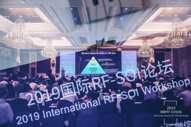
The SOI Consortium’s China 2019 event ran for two days, and it’s taken four (!) posts to cover all the presentations. In this final post we cover the afternoon RF-SOI sessions, which were dedicated to the China RF-SOI ecosystem and the RF value chain. In case you missed them, our previous posts recapped: 1. major keynotes from both the FD-SOI and RF-SOI days; 2. the FD-SOI presentations; 3. the morning sessions of the RF-SOI day; and 4. (this post) the RF-SOI day afternoon sessions. As we noted in Part 1 of our RF-SOI coverage, there were over 500 attendees for the RF-SOI day. And impressively, the room was still packed right through to the very end of the afternoon. Read on! SESSION 2: CHINA RF-SOI ECOSYSTEMSuzhou HunterSun Electronics: Super Opportunity for Integrated RFFE (“Jacky” Yujun Ding, COO)This talk had two parts. First, how is 5G changing the world, and second, what are the RFFE opportunities? He cited IHS data indicating that 5G will create tens of millions of jobs. New products include NB IoT, cellular V2X, as well as traditional PC/tablets and smart phones. But you still need to cover 2/3/4G with 5G. Major growth will happen in 2025-27. In terms of opportunities for RFFE, you've currently got 550mm2 going for $8; in 5G, you'll need 600mm2, but it will cost $16. You need RFSOI for filters and antenna switches, which are in high demand. Parts of the supply chain have no China players. Revenue for BAW is higher than SAW, but there's more SAW. He sees the industry moving heavily into integrated FEM (versus chip-on-board). He finished by itemizing different parts of the RFFE, indicating where the opportunities are (citing some data from Yole), with a special emphasis on integrated products for Chinese companies, with continued investor confidence. SmarterMicro: RF-SOI: Key Technology of Smart Connection (Yangyang Pen, Director) RF-SOI is an enabler of smart connections. However he sees GaAs as better for power, so SmarterMicro has a solution combining RF-SOI and GaAs. They've developed the world's first mMTC RFFE for high-performance upgrades on a single die and software reconfigurable. He notes that for IoT, lifetimes will be longer than 10 years, and that terminals are becoming more powerful. CanaanTek: Critical SOI CMOS Blocks in the 5G NR Sub-6GHz RF Front-End Architectures (Wayne Ni, CTO Board Chairman) CanaanTek is a fabless company working in consumer markets, with switches, tuners and LNAs in SOI-CMOS. He wants to capture 10% of the market with a focus on sub-6. The antenna/tuner is a must, and they've developed solutions for switches here. The figure of merit is RonCoff. He showed a product roadmap on SOI-CMOS. Xpeedic: Innovative EDA Solutions to Enable Differentiated RF-SOI Designs (Feng Ling, CEO)RF-SOI is growing, but there are still design challenges in process, models, filters and packaging. To design a good front end, you need better models and filters. People think passives are easy, but you need accurate models here. Xpeedic has developed design flows that include the effects of packaging early in design. Their products include IRIS, iModeler and Metis (for packaging). They've also introduced substrate modeling in partnership with CWS in France. The product is called SiPEX: it can address linearity in switch or PA designs. You need accurate substrate models to do this. Customers indicate they're seeing big improvements as well as reductions of 25% in chip area. IDP filters is another place they're working, to provide RF filters to fabless IC or module companies. No single filter technology can fit all the needs – IDP is one of them, so they have a broad portfolio of IDP filter technologies. He closed by saying that especially in China, the SOI ecosystem is really growing. SESSION 3: RF VALUE CHAINTowerJazz: Specialized RFSOI Foundry Technology to Support Rapid New Product Development (Paul Hurwitz, Director of RF Technology Development)This presentation gave a full overview of what TowerJazz offers in terms of RF-SOI foundry services with its fabs in Isreal, the US and Japan. What's new in 2019 is a diversifying of 200mm and 300mm. 200mm is best for power handling (for infrastructure/basestation antenna tuners and switch power handling, for example). 300mm is best for SW and LNA integration and higher digital densities. They've got new SOI models for the latest technology generations, and physics-based modeling of RF breakdown for accuracy. With more die being flipped, they needed new substrate modeling. For LNA and switch integration in 300mm, they invested in RF modeling. They also have an in-house MPW (multi-project wafer) program. He noted that customers in China are moving quickly in response to their customer requirements. Okmetic: Tailored Silicon Substrates for RF Applications (Atte Haapalinna, CTO)Okmetic Oy is a niche player in the substrate materials market, with specialties in sensors and MEMS, where they are the market leader. Now part of China’s NSIG group, they are expanding their manufacturing facility in Finland. In this presentation, their CTO talked about their current offerings as well as what they have under development. They do 150-200mm wafers, with a special emphasis on thick SOI. In terms of silicon substrates for RF, ultra-high resistivity is key. Their wafers are also used in IDP – integrated passive devices – for RF and acoustic filters. They are continually improving their high resistivity Magnetic Czochralski (MCz) silicon wafers, and are developing substrates for RF passives for automotive V2X. For RF beyond 6 GHz, they are looking at customized high resistivity silicon wafers for mmWave with researchers and customers. For sensors, they do SOI wafers with built-in cavities. Incize: RF SOI Ecosystem – History Challenges (Mostafa Emam, CEO)The world is exceeding expectations in terms of data usage. While the CAGR for devices is 27%, for data it’s 46%. Therefore each device needs to be faster and more power efficient. Incize recognizes RF as an art, with each piece hand crafted. But artists need to see the whole picture: at Incize, they help 17 companies – including wafer suppliers, foundries and fabless – see that big picture, especially in measurement, characterization and modeling for RF. For wafer suppliers, they do very high-power and very precise on-wafer testing to determine things like intermodulation distortion and substrate interference. For foundries, their specialty is in RF switches, for whom they do harmonics testing and thermal noise management. With those insights, Incize foundry customers have drastically increased the performance of the RF chips they’re manufacturing on trap-rich, high-resistivity SOI wafers. Meanwhile, Incize is also preparing PDKs for future potential substrate generations including GaN-on-Silicon, silicon-on-porous, and new contactless testing techniques for piezoelectric-on-insulator (POI – used in filters in 4/5G). “There’s a really big business opportunity for RF-SOI,” concluded Emam, “and room for everyone.” Cadence: SOI Technology in Intelligent and IoT/Vision/AI Systems (Jonathan Smith, Senior Director)Cadence does SOI enablement at advanced nodes. Smith shared three recent success stories. First, there’s the Musca-S1 test chip they did with Arm, Samsung and Sondrel this past spring. Second, there’s the Tensilica DSP for automotive vision on GlobalFoundries’ 22FDX, which uses 1/10th of the power of existing solutions and was demonstrated at CES. And finally there’s the i.MX line from NXP. In recent news, there’s a new version (18.1) of Virtuoso RF. Though it’s been on the market for 30 years, they’ve added advanced methodologies so that system design and analysis are on the same platform. They’ve also announced National Instruments’ analysis solver, the Clarity 3D solver for next-gen 3D solutions, the integration of multiple electromagnetic (EM) solvers, and advance SiP options. Silvaco: Xena-IP Management Infrastructure for the SOI Ecosystem (Babak Taheri, CEO)Every multi-core SoC today has as many as 200 IPs, if not more. How do you manage that? Tracking and traceability of IP is complicated but important. For IP providers, how do they track where its being used? And for IP consumers, they need to know what they’ve used and where. What’s required is an IP management system to keep track of the different functions and different concerns. Today’s tracking systems don’t talk to each other. Silvaco’s Xena IP management solution organizes all IP data, accounts, products, contracts, devices, support, compliance and reporting. For compliance in particular, they do IP “fingerprinting” and “DNA analysis”, which they’ve patented. The fingerprint is a digital representation of the IP: it’s not just software. It is secure, and can’t be reverse engineered. It’s not a tag: a tag is inserted into the IP, whereas fingerprints are extracted. DNA analysis flags discrepancies and quickly identifies where they are and which files to look in. Xena works in the cloud, enterprise systems or hybrids. The SOI ecosystem will be hearing a lot more about this. ~~ Please note that the China event presentations are all available on our website to anyone whose company or organization is a member of the SOI Consortium.
Read More
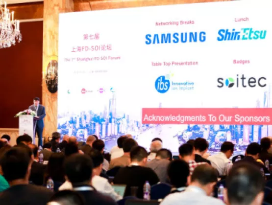
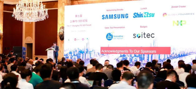
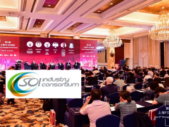
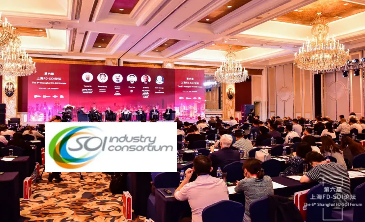
The first day of the SOI Consortium’s recent China event – the 7th Shanghai FD-SOI Forum – was full to bursting in every way: the room, the networking, the level of expertise, the in-depth presentations and the overall energy. We covered the Samsung and GlobalFoundry keynotes in our previous post (if you missed it, read it here).This post will recap the rest of the presentations given during the day. (If your company or institution is a member of the SOI Consortium, you’ll be able to access the full presentations online.)International Business Strategies (IBS) – Impact of AI on Automotive and IoT, and Opportunities in China (Handel Jones, CEO) When it comes to deep insights on China + tech + analytics, and especially with a thorough understanding of FD-SOI markets, Handel Jones is arguably the world’s leading expert. Here are some of the observations he shared. Though the chip industry will see declines across the board in 2019 (he sees 13.5%), he sees a return to growth in 2020. By 2030, he sees it as a trillion dollar market, of which China will have half. AI is a key driver – and will become more prevalent at the edge. Major drivers will include preventative medicine, gaming, NB-IoT and 5G. At the chip level, FD-SOI has a lower cost/chip compared to bulk – you’ve got small chips and high yields. Sensors – especially image sensors – are a key area, and this is another place where FD-SOI is better than bulk. He sees chip shortages in the 2022-24 time frame (as opposed to the current oversupply), so now is the time that China should be establishing large FD-SOI capacity.NXP – Automotive, Industrial and IoT Solutions Leveraging FD-SOI (Ron Martino, VP GM) In terms of power consumption, computing is easy but data transmission is hard, Ron Martino reminded the audience at the onset. That’s why you need the edge. This is where FD-SOI comes in, and if you want to have leadership, you should be leveraging body biasing, he said. In terms of machine learning, a lot can happen at the edge on the smallest devices. NXP is now shipping a very wide range of products based on FD-SOI, including the i.Mx7 and 8 families and the new RT crossovers. The latest announcement is the i.Mx RT 1100 MCUs, a very low-cost processor solution for high volumes. The i.MX7 ULP is in mass production for wearables, with record low leakage and high performance. The i.Mx8 and 8x are going into a broad range of applications – from retail solutions for automated checkout to pasta makers, and automotive applications for full cockpits with vision detection, as well as things like parking, V2X and in-vehicle monitoring.Sony Semi – Low Power IoT Products with FD-SOI eMRAM Technology (Kenichi Nakano, GM) Chips built on FD-SOI with eMRAM are in production, said Kenichi Nakano. In GNSS/GPS, Sony is the #1 in lowest power consumption worldwide, thanks to FD-SOI, he continued. They’ve had 70 remarkable design wins, giving them over 50% market share in the sports and health watch markets, he said with a tip of the hat to the FD-SOI ecosystem and SOI Consortium. In GNSS, performance is very important – and now they can do it in water, which is huge. Development cycles are shorter than ever – for the latest chip it started in February 2018 and was in production by the spring of 2019, achieving decreases of 20% in power, 30% in area and 10% in cost. Integrating eMRAM was easy in terms of the design flow and manufacturing, with production yield of 97-100%. So with the GXD5605GF they’ve got the first GNSS chip with FD-SOI/eMRAM/RF in the world and it’s on 28FDS/eMRAM technology. It’s very reliable and very good, he concluded.Rockchip – Challenges of AIoT Chip (Feng Chen, SVP) At the beginning of this year Rockchip announced the launch of their RK1808, a low-power AIoT solution with built-in high performance (3TOPS) NPU fabbed in GlobalFoundries 22FDX, said Feng Chen. Their clients were very happy that Rockchip delivered the real power and performance numbers they’d promised. Because of the power/performance it delivers, FD-SOI (both 22 and 28nm) is very well suited for AIoT chips, he said. It’s very cost-effective in terms of NRE and die, and there’s room for further savings. While the ecosystem needs a unified push, FD-SOI is good for the market in China, and China has the volumes FD-SOI needs. Rockchip sees particular potential in retail and smartphones.Panel – Verticals Driving FD-SOI VeriSilicon CEO Wayne Dai moderated the first panel, asking first why China should adopt FD-SOI. Soitec CEO Paul Boudre said because it is a big, dynamic market (noting that Sony’s first FD-SOI GPS win was in China). Handel Jones said that at the wafer level, there was cost parity, but with FD-SOI chips are smaller and higher yield. The main reason it’s taken so long to get going was IP, but that’s changing now, he added. Dai’s next question was about the top application fields the panelists predicted for 2020. Sony’s Kenichi Nakano said wearables with connectivity, low power consumption, small size and high levels of integration; Rockchip’s Feng Chen agreed. NXP’s Ron Martino said FD-SOI for automotive, machine learning and edge computing was shipping now, with wearables ramping.VeriSilicon – Low Power IoT Connectivity IP Design Based on FD-SOI (Yi Zeng, Director, IoT Connectivity Platform) The “value” of IoT data is not yet being generated, noted Yi Zeng but AI can help here. The IoT industry needs innovation for both chips and networking. SiPaaS – which stands for Silicon Platform as a Service – as offered by VeriSilicon can help lower the barrier to entry. [In the SiPaaS model, VeriSilicon has its own IP-based core. Based on the company's advanced chip design capabilities and mass production service experience, it has created a variety of silicon-proven chip design platforms that can significantly reduce the customer's chip design cycle.] They have FD-SOI IP for NB-IoT, BLE, GNSS and sub-1 GHz. The BLE (Bluetooth) RF IP is a complete offering optimized for low power on GlobalFoundry’s 22FDX. The NB-IoT IP is also optimized on their 22FDX ZSPNano, an energy efficient general purpose MCU+DSP core on 22FDX. And they’ll have results of test chips for GNSS RF IP on 22FDX by the end of this year.Secure-IC – AIoT Embedded Security Using FD-SOI (Hassan Triqui, CEO) While AI enables products and services, it’s important to plan for security early in the design cycle, said Hassan Triqui. Software is not enough to protect edge-to-cloud. Secure-IC’s hardware security module, Securyzr, is an IP block that can be embedded into every device to answer security functionalities such as root-of-trust and key management. In sleep-mode/tunable cryptography, FD-SOI allows the creation of physically secure systems. (Note that designers are leveraging FD-SOI’s unique body biasing for ultra-low-power deep-sleep modes.) Because safety and privacy require a combined solution, Securyzer is particularly well-suited to IoT chips built on FD-SOI, he concluded, so that IoT adds value to AI, and not just the other way around.Soitec: FD-SOI – The 5th Gear for mm-Wave Radio (Michael Reiha, GM FD-SOI Business Unit) There are four key areas to 5G, explained Michael Reiha: coverage, number of antennas, frequency and traffic density. 5G mmW access architectures are currently inefficient in terms of power and performance, but FD-SOI is ready for 5G access as both an analog and hybrid beamformer. For MU-mMIMO (massive MIMO), the RF front-end modules (FEMs) and transceiver will fully exploit FD-SOI. Sensing, calibration and control enabling hybrid beamforming and multiple users is easy in FD-SOI. The adaptive body biasing on the horizon will reduce power of FEM mixed-signal circuitry, and be a disruptive technology.STMicroelectronics – Automotive MCUs in 28nm FD-SOI for ePCM NVM (Shan-Lin Liu, Automotive Marketing Manager) As a leader in the automotive market, ST has seen that increased data flows in automotive are driving demand for higher performance and bigger memory in automotive MCUs, said Shan-Lin Liu. ST has taken a unique approach to NVM with embedded PCM (phase change memory) on 28nm FD-SOI. This gives them energy-efficient, high-performance cores with larger NVM memories, and it’s already qualified up to auto grade-0. PCM (vs MRAM) is BEOL. It uses two cells, so it’s more reliable and is good at high temperatures, he said. With FD-SOI, they can go up to 165o, and it’s soldering compliant. The preliminary results of the first MCU chip are excellent. It’s now running in a car, replacing the previous generation 40nm eFlash product.Leti – Advanced FD-SOI for Edge AI (Emmanuel Sabonnadiere, CEO) To fully run artificial intelligence on the edge, research powerhouse Leti is working on an unsupervised learning neural network using advanced FD-SOI and a mix of other technologies. These include embedded non-volatile memory (NVM), 3D integration, and new design tools. Sabonnadière said this new approach is expected to exceed the performance levels of current digital deep learning with neural networks that are capable of handling time-domain signals, sound and speech—and may produce a first "killer app" for advanced SOI. AI will require compact and power-efficient circuits for the inference phase, when neural networks infer things based on new data they receive, close to the end user. The combination of FD-SOI, 3D integration, and NVM opens a path towards dedicated circuits with major performance improvement within the limited power budgets of distributed electronics. In Europe, he noted, privacy concerns are driving the move from the cloud to the edge. On the Leti roadmap, they’ve broken through the 10nm limit for FD-SOI, using strain and body biasing to compensate for transistor mismatch. Also of note: since 2016 Leti has had an ongoing collaboration with SITRI, the Shanghai Industrial μTechnology Research Institute, an international innovation center focused on globally accelerating the innovation and commercialization of More than Moore technologies to power IoT.GlobalFoundries – GF Fab 1 Dresden: Delivering Differentiation with FDX for the Future of Automotive (Thomas Morgenstern, SVP GM Fab 1) Dresden Fab 1, Thomas Morgenstern reminded the audience, is the biggest in Europe, where it is part of the Saxony ecosystem. GF is moving advanced mask-making to Dresden, which is the lead site and Center of Competence for FD-SOI. With the “pivot”, GF is providing platforms. Fab 1 is automotive certified for 22FDX (GF’s 22nm FD-SOI technology), with automotive tapeouts in 2019. “Automotive is a journey,” he said, of continuous improvement, and a mindset: it’s a zero defects culture. The ramp to volume production is well underway, with 26 tapeouts of 22FDX products this year – almost double that of last year. He showed high yield data of about a dozen products, adding that since the beginning of the year every tapeout was first-time right with decreased cycle time. The key specifications for 22FDX with eMRAM for Auto Grade-1 have all been demonstrated, and customer feedback has been excellent.Next: Shanghai International RF-SOI Workshop recap As you can see, it was a packed day for the FD-SOI part of the SOI Consortium’s Shanghai event. In fact the room was still packed at the very end of the day. Several hundred VIPs then headed out for the ever-popular and festive evening riverboat dinner cruise, where the non-stop networking continued.A big shout-out to our sponsors and supporters: VeriSilicon, Simgui, SIMIT, Soitec, Samsung, IBS Ion Implant, ShinEtsu, GlobalFoundries and NXP.The next day of the event was devoted to RF-SOI. That will be the subject of our next post.
Read More
The ESG MarketElectronic Gases represents the largest percentage of the spend on chemicals and materials by semiconductor producers. Taken altogether, the spend on Electronic Gases was almost $6 billion worldwide in 2018. Recent critical shortages of key gases have impacted the industry tremendously and, in some cases, has also limited output. The Electronic Specialty Gas (ESG) market, while a small segment of the global gas market, is one of the most complex and least understood market segments of the electronic chemicals and materials landscape. Linx Consulting estimates that the ESG market totaled nearly $3.4 billion in 2018, up from roughly $3.1 billion in 2017 with a growth rate of 10 percent last year. Growth was driven by rising demand and the increasing use of higher-value products in applications such as etch and specialized deposition. ESGs are used in the manufacture of electronic devices that are subsequently assembled in systems and in a variety of processes such as film deposition, film etching, substrate doping and chamber cleaning. The devices – semiconductors, LEDs, and displays – are processed on larger substrates, and then separated before assembly.Key differentiators for ESGs are not only the technical complexity of the gases and mixtures supplied, but the purity and consistency demands placed on the gas supply. Product purity and consistency, often at the limits of analytical capability, must go hand in hand with rigorous application of statistical process control in manufacturing and absolute delivery reliability. ESGs include fluorocarbons, hydrocarbons, deposition precursors, dopants, corrosives (halides/hydrates) and rare gas mixtures.The key end-use markets for ESGs include semiconductor wafer fabrication, flat panel display (FPD) manufacture, compound semiconductors / LEDs production and Photovoltaics cell manufacture, as illustrated below in Figure 1. Figure 1 - ESG Market by End-Use Applications Source: Linx Consulting The semiconductor industry is the largest user of ESGs and has the most diverse ESG requirements in terms of products, package sizes and purity requirements. The semiconductor industry uses all the different specialty gases produced. Purities are typically 4N and above and the packages can range from small cylinders to tonner/Y packages to tube trailers. The ESG market is global, with key demand centers in China, Europe, Japan, Korea, Southeast Asia, Taiwan and the United States. The Flat Panel Display (FPD) community is the second largest user group for ESGs. However, the breadth of ESG products used in FPD fabs is much more limited than in the semiconductor industry. Key product applications include silicon sources, dopants, oxidation and nitridation sources, chamber cleans, and etchants. ESG use has grown with the development of the FPD industry across both TFT-LCD segment and AMOLED segment, with many large end users in Korea, China, Taiwan, and Japan. Korea and China boast large ESG supply infrastructures geared towards serving the FPD industry. Early on, these countries targeted the development of the FPD industry and the associated value chain, so there has been large-scale development of required ESG products such as NF3 and silicon precursors. When we review the markets in aggregate, coupled with the geographic intensity of the electronics industry in Asia, it is unsurprising that a vast majority of the ESG market would be in Asia, as illustrated in Figure 2, below.Figure 2 - ESG Market by Key RegionSource: Linx Consulting Key ApplicationsThe applications for ESGs can be readily tied to major thin film fab processes that are commonly used in the microelectronics industry. The processes include dielectric and metal etch, dielectric deposition, metal deposition such as titanium or tungsten, deposition of non-silicon materials such as hard masks etc., dopants for thermal diffusion methods and ion implantation, reactor chamber cleaning; as well as some other specialty applications. This is illustrated in Figure 3 below. Figure 3 - Applications for ESGsSource: Linx Consulting Clearly there is a close tie-in for ESGs into thin film deposition (CVD and chamber cleaning) and etch processing. In the future, the industry will increase its use of ESGs with novel deposition and etch processes. New applications may include lower temperature deposition, high deposition rate processes, flowable CVD films for high aspect ratio structures, and high selectivity deep etching with greater uniformity. All these processes improve device performance and will rely on ESGs and rare gases as enablers. Outlook for ESGsOverall, we believe that the ESG market will grow at a compound rate of about 6 percent over the next five years. Currently the largest six suppliers – Versum Materials, SK Materials, MTG/TNS, Air Liquide, Linde/Praxair, and KDK – control about half of the overall market, with about 50 suppliers accounting for the other half of the market. We anticipate that as the industry continues to grow, we will continue to see changes in the supplier base with both continuing consolidation and new regional suppliers emerging as unique technologies and value-added capabilities enter the market.For More InformationThis article is based on insights and analysis from Linx Consulting’s Electronic Specialty Gas report. The annual report is considered the leading industry source for comprehensive information about demand for specialty gases used in the electronics industry. We track more than 60 different ESG products used across the global semiconductor, flat panel display, solar and compound semiconductor industries.For more information, please contact [email protected], or Mike Corbett at +1 973 698 2331, Mark Thirsk at +617 273 8837, or Andy Tuan + 886 952 111222, or visit Linx Consulting.Interested in engaging with the electronic materials supply chain? The Electronic Materials Group (EMG) is a SEMI technology community representing SEMI member companies that provide substrates, polymers, metals, organic and inorganic materials, chemicals, and gases developed for electronics manufacturing. Linx Consulting has been a longtime member and supporter of the SEMI Electronic Materials Group.Mike Corbett is managing partner and Andy Tuan is managing director, Asia, at Linx Consulting.
Read More
The recent SOI Consortium’s FD-SOI and RF-SOI events (Shanghai, September 2019) were record-breakers, with attendance approaching 1000 over the two days. The event was extensively covered in the China tech press, which often cited the opportunities SOI-based technologies offer for technology leadership. Indeed, as SOI Consortium Executive Co-Director Carlos Mazure noted in a follow-up press conference, the SOI technology drivers dovetail perfectly with the semiconductor industry’s top growth drivers*: IoT, 5G/smartphones, AI/ML and automotive. Here are the takeaways he cited from the China events:SOI for AIoT, consumer and automotive: the FD-SOI ecosystem is in place (substrate supply, foundry offering, EDA and design IP). The 1st wave of adoption is ramping at NXP, STMicroelectronics, Sony, Rockchip, Synaptics, Renesas and more Fast followers are lining up, with the number of tape-outs increasing at Samsung and GlobalFoundries SOI for 5G: development is driven by the need for low cost, low latency and high data throughput the SOI ecosystem for 4G/5G technologies is in place with a strong market pull RF-SOI, the reference FEM 4G technology, will extend its benefits to sub-6Ghz: low power consumption, high linearity, low insertion loss, co-integration of RF components. 5G mmWave requirements are addressed by multiple SOI platforms (RF-SOI, PD-SOI and FD-SOI) enabling integrated analog mixed signal solutions at low power consumption. Two RF-SOI luminaries were honored at a post-event dinner sponsored by China wafer purveyor, Simgui. Jim Cable, Chairman and CTO of pSemi, a Murata Company, and Herb Huang, CEO and GM of Ninbo Semiconductor received awards for their contributions to the advancement of RF-SOI (more on this later). There’s an enormous amount to tell you about from the conferences, so this will be the first round-up post of several.Gitae Jeong, SVP, Samsung Electronics (Courtesy: VeriSilicon live.photoplus.cn) But briefly, in his talk entitled, "IoT Platform with FDSOI", the main points made by Gitae Jeong, SVP, Samsung Electronics were: 28FDS is fully mature. It has the same design rules as bulk, has an integrated security key, a wide range of packaging options for IoT, and a design guide that makes back biasing easier and simpler with complete IP solutions. 18FDS development is on track for this year, with 14nm BEOL and a 35% increase in performance, a 55% decrease in power (!) and a 35% decrease in area compared to 28nm. 1st products are now shipping with eMRAM on 28FDS with yields over 90%, operating temperatures have been extended to 125C for automotive, and a 1Gb version has been demo’d. 1st 5G products mmWave products on 28FDS are now available Americo Lemos, SVP, GlobalFoundries (Courtesy: VeriSilicon live.photoplus.cn)In his talk, "Leading Industry Innovation by Differentiated SOI-based Solutions", key takeaways made by Americo Lemos, SVP, GlobalFoundries included:They have leadership in RF-SOI, with over 50 billion chips shipped 22FDX (FD-SOI) is in production. Last year they had 14 tape-outs, this year they had 26 – half of which are for companies in China. By the end of this year they’ll have shipped 100 million good dies to customers, marking the full transition from ramp to volume. In the ecosystem, they’ve got 285 IP titles from providers worldwide, with more announcements coming soon. Work continues on 12FDX – more to come on this. Edge AI is the next growth engine for IoT, combining vision + voice + audio, with China coming in strongly with ultra-low-power design for home connectivity, industrial, personal and medical applications. The RF-SOI day was lead off by the reading a letter from Dr. Xi Wang. The leading proponent of SOI in China for over a decade as head of the Shanghai Academy of Sciences, he’s now the country’s Vice-Minister of Science Technology. Until this year, he’s always had the first keynote at the SOI Consortium events in China, but this time he was in a meeting with the VP of Russia. However, his warm letter confirmed his support for the SOI ecosystem, especially the role of SOI-based technologies for China in the 5G era. Danni Song, China Mobile Project Leader. (Courtesy: Simgui live.photoplus.cn) This was followed by a talk by the ever popular and insightful Project Leader Danni Song of China Mobile, the largest of the operators there. China issued 5G licenses in May 2019 as the country gears up for 5G commerce. By next year, 5G will be deployed in all cities above the prefecture level. For now, it’s all about sub-6GHz. The challenge, she noted, is in power consumption, which is 2-3x that of 4G in base stations and devices. They see two development spaces: one for consumer and one for verticals, and have teamed up with Sprint on a 5GS (S being for Superior) module. They released a basic modem chip and dongle in June, and a smart chip is coming. She suggests people consult the China Mobile white paper on 5GS for more info. We’ll cover the many other presentations over the next few weeks – so stay tuned! --------*as cited in a 2019 CEO survey by KPMG/GSA.
Read More
Despite market saturation and stagnation saddling many business sectors, MEMS remains a shining star in the semiconductor industry. Opportunities in automotive, consumer electronics, mobile, medical are rising. What is supporting this industry growth? Who are the big players on the horizon?SEMI spoke with Dimitrios Damianos, Technology Market Analyst, Photonics, Sensing and Display division at Yole Développement, about MEMS market dynamics and future trends. Damianos shared his views ahead of his presentation at SEMI MEMS Imaging Sensors Summit, 25-27 September, 2019, at the WTC in Grenoble, France. Join us at the event to meet experts from Yole and many other key industry influencers. Registration is open.SEMI: MEMS and sensors is one of the healthiest industries not only in Europe but globally. Despite a global economic slowdown, the MEMS and sensors is still growing. What is fueling this growth?Damianos: The value of the global MEMS and sensor market will almost double from $48 billion in 2018 to $93 billion in 2024. In 2018 the MEMS and sensor market represented more than 10% of the total IC market, as more and more MEMS devices and sensors, such as MEMS, image sensors, and RF filters, are integrated in end products in consumer and automotive. In particular, the value of the MEMS-only market reached $11.6 billion in 2018, with consumer applications accounting for more than 60% of the total market. From 2019 to 2024 the MEMS market will grow 8.3% annually in value driven by pressure (for TPMS), RF (for V2X 5G communications), inertial (for ADAS) and future MEMS (such as pMUT for ultrasonic fingerprint) (Source: Status of the MEMS Industry report, Yole Développement, 2019). SEMI: How are MEMS shaping the semiconductor industry today? Damianos: MEMS have a make-smarter enabling capability. They are providing context for new applications and services in transportation, mobility, health, and security. Large companies such as Alibaba and Google are considering MEMS as a critical element in their business solution domains covering the upcoming smart home, smart campus, smart city and smart industry applications. MEMS have key features that correspond to these companies’ criteria for accuracy, small size (without performance degradation), low power and always on (e.g. microphones). Furthermore, with the advent of sensor fusion and edge computing, more sensor data can be processed, maximizing the qualitative and useful information about us and our surroundings. This has a huge impact in all markets, especially consumer.SEMI: MEMS foundries performed well thanks to the boom in industrial and medical applications. Who are the big players right now?Damianos: During 2018, all foundries saw their revenue increase. STMicroelectronics, Teledyne Dalsa, Silex, IMT, Micralyne and Philips Innovation Service are important MEMS foundry players that offer services for various MEMS devices used in medical and industrial markets, among others. On one hand, medical applications were driven mostly by microfluidics, flowmeters, pressure and inertial MEMS. On the other hand, industrial applications were driven by inkjet heads, microbolometers and pressure MEMS. The market prospect, however, is huge for RF MEMS and oscillators that will be used in next-generation 5G infrastructure. SEMI: What is the current status of MEMS for automotive applications? What are the related market drivers? Damianos: In automotive applications, accelerometers and pressure sensors still account for the lion’s share in units. Pressure sensors will grow at more than 8% with Tire Pressure Monitoring System (TPMS) implemented in Chinese vehicles in the near future. After 2019 and 2020, with the new Chinese standard, GB 2614, TPMS will become compulsory: 100% of all new vehicles will have TPMS. Also, automotive MEMS could grow quicker than the corresponding car market (currently at approximately 3%). The reason is a higher number of many different MEMS devices that are being integrated in cars, such as MEMS inertial measurement units (IMUs), TPMS, environmental MEMS for gas and particle monitoring in-cabin and microphones for hands-free voice commands.SEMI: After years of decline, the inkjet heads industry is growing again. What other segments are benefiting from MEMS technology applications? Can you name two examples?Damianos: RF MEMS (BAW filters) is also benefiting from applications in smartphones and will continue to benefit with the arrival of 5G. 5G means additional high frequency sub-6 GHz bands that can only be addressed by BAW filters. Moreover, new infrastructure approach using active antennas will create an expanding market for BAW.Another segment is inertial sensors. Inertial MEMS already have a high potential in wellness and fitness wearables and are gaining support for medical wearable applications to monitor patient activity, with the aim to prevent seizure in cases of epilepsy and other mental disorders. Compared to other types of sensors, MEMS is the golden technology for inertial sensors integrated into medical wearables. They are used for rehabilitation systems, activity trackers and assistance living/fall detection. Specifically, the IMU market will continue to grow for consumer and automotive applications as their price and form factor continue to shrink and they replace traditional standalone MEMS accelerometers and gyroscopes. However, the inertial sensor market will mostly grow for smartphone applications (mostly 6DOF, with 9DOF volumes being comparatively low).SEMI: Give us one prediction about the opportunities offered by the MEMS technology. Damianos: Sensor fusion is becoming more and more relevant since billions of MEMS sensors are made every year. The upcoming 5G revolution will make connectivity easier than ever, creating exponentially more data. To make these data meaningful, data processing is mandatory. Big data is an industry born of recent advancements in AI and machine learning, built upon and fueled by a wealth of new data from ever-expanding sensor applications. An upcoming trend is edge computing, with sensors and MEMS driving a new age of technology. Sensors are digitizing the human experience, and as the real and virtual worlds move closer together, it will be sensors that bind them, enabling new experiences for users everywhere. Running AI at the edge, coupled with sensor fusion, will open new applications for MEMS in audio, motion, olfactometry, and imaging. We also expect that new MEMS devices (microspeakers, ultrasonic fingerprint, pMUT) and piezoelectric MEMS technology could rejuvenate the MEMS market. SEMI: What are your expectations for SEMI MEMS Imaging Sensors Summit and why would you invite your peers to attend? Damianos: SEMI is organizing another very successful event, gathering experts from the Imaging and MEMS industries. We are at a turning point of innovation, with many technological advancements in AI, IoT, AR/VR, biometrics, and other areas where Imaging and MEMS technologies are paramount. Yole is excited to hear the thoughts of many high-profile experts on existing activities and future prospects within their organizations. If you are too, then it is an event that you shouldn’t miss!Dimitrios Damianos, Ph.D. is a Technology and Market Analyst in the Photonics, Sensing and Display division at Yole Développement (Yole). Damianos is a member of a Yole team that produces technology and market reports on the imaging industry including photonics and sensors. Damianos holds a MSc degree in Photonics from the University of Patras (Greece). After his research on theoretical and experimental quantum optics and laser light generation, Dimitrios pursued a Ph.D. in optical and electrical characterization of dielectric materials on silicon with applications in photovoltaics and image sensors, as well as SOI for microelectronics at Grenoble’s university (France). He has also authored and co-authored several scientific papers in international peer-reviewed journals. Learn more! Join the webinar on 5th September 2019. Registration is open! Serena Brischetto is a marketing and communications manager at SEMI Europe.
Read More
Flexible hybrid electronics (FHE) is innovation and modern technology at their best, giving rise to lighter, more malleable sensors that better conform to the human body while breeding new applications across a number of markets. For the semiconductor industry, FHE technology is enabling the development of a new generation of chips with the high performance, light weight, scalability, softness and flexibility usually seen in printed electronics. The technology is a boon to chipmakers, giving them novel ways to innovate for the Internet of Things (IoT) market.“The global printed electronics market is expected to garner 14.9% GAGR from 2018 to 2023,” said Stanley Wong, Director of Asia Business Development, Brewer Science, said in his presentation at FLEX Taiwan 2019 in late May. Representatives from industry, government, academia and research institutions gathered at the event in Taipei to explore flexible electronics innovation and growth opportunities.One shining star of FHE innovation is the foldable smartphone. So bright is the future of the bendable devices that not even recent trade tensions between the United States and China have dimmed prospects for the fledgling industry.“While the US-China trade war might slow down shipments of Huawei’s phones, the industry remains bullish on foldable phones,” said Stacy Wu, Principal Analyst at IHS Markit. “When the first generation of flexible AMOLED displays was launched in 2016, the rolling radius was 3mm and it could be folded 200,000 times.”For foldable phones, the 200,000 mark was a major milestone – the industry’s consensus standard for foldable phone display reliability. The industry reasoned that phones capable of being folded and unfolded 200,000 times without distorting color or images or the display itself cracking was a safe bet for consumer adoption. Earlier this year, both Samsung and Huawei announced foldable phones using the thin-film-display technology, ushering in the era of mass-market availability of the devices. Steve Chiu, Division Director for Electronics, IC package, Industrial Technology Research Institute (ITRI), believes that breakthroughs in the next generation of flexible AMOLED technology will allow thin films to be folded 100,000 times with a rolling radius up to 30mm and electric resistivity of less than 10 percent. The rolling radius of 30mm, 10 times higher than today’s phones, will give foldables a higher bending radius, while the lower electric resistivity will help maintain the brightness of the AMOLED panel after tens of thousands usages and extend the service life of foldable smartphones.The biggest challenge facing the foldable phone industry remains developing new materials that are flexible yet durable, stressed Francesco Lemmi, Business Development Director, Flexible Display, at DuPont. Today, the prevailing practice is to layer polyimide (PI) and hard coating on the display module. These stacked protective films replace traditional glass panels but present technical challenges related to impact resistance and the durability of the display as it is folded and unfolded over time.Smart clothing market is another hot market, with 33 percent global growth annually and revenue expected to reach US$ 3.26 billion in 2026. Yet for all the promise of smart clothing, reliability and accuracy remain a big challenge chiefly due to a lack of industry standards. Another gap is the unanswered question of whether consumers will embrace light and energy-efficient products.FLEX Taiwan 2019 speaker Satoshi Maeda of Toyobo is confident they will, pointing out that in the future consumers will enjoy a wide selection of comfortable smart clothing products and applications. The industry is still working to better understand how to develop human-machine interfaces, the essential seam between the human body (the outer layer of skin) and electronics, said Dr. Reinhold H. Dauskardt of Stanford University. Still, he sees great promise in an innovative somatosensory communications platform involving human skin. Human-computer interactions have historically been defined by human touch and vision (for example, typing at a computer keyboard and checking our monitor for the accuracy of our inputs). Dauskardt believes that, in the future, electrical impulses from the skin (conductance) will interact with signals from electronic devices to establish a more intimate human-machine interface that could be adapted one day to extend the visual and auditory abilities of humans.David M. Yeung, co-founder and CEO of Lionrock Batteries, pointed to another challenge in wearables: battery size. Today, large and heavy batteries account for 50 percent to 70 percent of the space in wearable devices, making many of the products too cumbersome to wear. Nanofiber lithium-ion batteries now under development can be as small as ultra-thin 2mm with a rolling radius of up to 20mm in radius and support for high electrical currents, significantly lightening their weight and improving comfort.Nardev Ramanathan, Lead Analyst, Digital Health and Wellness at Lux Research, predicts that, of all flexible electronics products, smart watches will win the largest market share and with the fastest rate of adoption. The devices will get a boost when they shrink as flexible batteries are integrated with the bands. The next wave of smart wearables will feature devices for exercise or medical monitoring. Already, FHE materials have led to advances in medical devices. One example is that smaller hearing aids are now possible thanks to flexible electronics and dressings used to promote skin regeneration, reduce wrinkles and remove scars.Gillian Ewers, VP Marketing at PragmatIC, sees fertile ground for FHE applications in IoT solutions. As FHE manufacturing costs drop, she believes IoT technologies will significantly deepen their penetration into a broad range of industries. For example, the number of electronic tags used in convenience stores worldwide will exceed 100 billion in 2025. Thinner than human hair and more durable than traditional wafers, these tags are expected to spawn a host of new business opportunities. FLEX Taiwan attracted more than 270 attendees from more than 30 fields including smart healthcare, e-paper, displays, system integration, automotive electronics, textiles, wearables, and avionics. On the first day of the event, industry, academia and research center representatives from the United States, Japan, China, Singapore and Taiwan gathered to discuss common goals on a range of FHE-related issues and deepen cross-regional cooperation. Like the FHE industry itself, SEMI-FlexTech remains focused on the future by strengthening cross-border cooperation to help manufacturers find killer applications and test profit-making models. For Taiwanese companies, the event will continue to provide insights on market trends, equipment, materials, advanced manufacturing technologies, product applications and new business opportunities, helping the organizations hone their competitive edge in the global market.Emmy Yi is a marketing specialist at SEMI Taiwan.
Read More
The U.S. on September 1 will levy a 10 percent tariff on $300 billion (List 4) worth of Chinese goods that until now were exempt from duties, President Trump said today. The trade action makes good on the U.S. president’s commitment to impose the new round tariffs in response to China’s failure to deliver on promises to buy more U.S. farm goods and to stop the flow of the painkiller fentanyl into the U.S. The 25 percent tariffs already in effect on $250 billion in goods will remain in place.The new list includes items used in the electronics industry but also encompasses retail products spanning the U.S. economy including clothing, toys and cell phones, exacting a more direct hit to U.S. consumers. A meeting between China and U.S. trade officials in Shanghai this week apparently did little to ease trade tensions. Both sides plan to meet again in September, though expectations for meaningful progress toward resolving their trade differences then are low.The U.S. believes China backtracked from commitments to changing its practices related to forced technology transfer and intellectual property theft. China denies making the pledges and insists on the removal of all tariffs as part of a settlement.The U.S. actions risk backlash from China including non-tariff barriers to trade such as licensing delays, more stringent business-related inspections, and an accelerated rollout of its unreliable entities list, China’s response to the U.S. decision to blacklist telecommunications giant Huawei. The list includes foreign companies, other organizations and individuals that China sees as national security threats or risks to China’s economy.SEMI will continue to urge both nations to reach an agreement consistent with its 10 Principles for the Global Semiconductor Supply Chain in Modern Trade Agreements. The principles encourage free and fair trade, open markets, and respect of IP among all players in the global electronics manufacturing supply chain.SEMI member companies impacted by the new U.S. tariffs or facing any new non-tariff barriers in China should contact Jay Chittooran, public policy manager in SEMI’s Global Advocacy Office, at [email protected] Russo is vice president of Global Industry Advocacy at SEMI.
Read More
2019 will be a busy fall for the SOI Consortium and our members.First off are the SOI Consortium events in Shanghai and Tokyo, which are very popular indeed. We now have the dates locations locked in, so you’ll want to mark your calendars:Shanghai: 16 17 September 2019, FD-SOI Forum / RF-SOI Workshop. Both days will be held at the Pudong Shangri-La Hotel in Shanghai. The first day will focus on FD-SOI. The second day is all about 5G and RF-SOI. These are huge events – to get an idea of the magnitude, you can read our coverage of the 2018 event. Tokyo: 30 31 October 2019, Japan SOI Design Workshops. This year both days of workshops will take place in the Yokohama Landmark tower. The first day will be devoted to FD-SOI; the second day turns to More-Than-Moore – especially photonics and MEMS. Last year’s workshops were packed with excellent presentations and panel discussions, which we covered here. The SOI Consortium and members will also be giving talks at Semicon Europa, which is being held 13 – 15 November 2019 in Munich, Germany. The programs are currently being finalized. As soon as they’re ready, we’ll be sure to let you know so you can register and/or share the news with your colleagues and clients. But in the meantime, make sure you save the dates.Would you like to check out the presentations given at Consortium events in previous years? If you hover your cursor over the Events tab at the top of our home page, you’ll get a drop-down menu of events for the last five years (we’re working on adding more – we’ve been doing these events for over a decade!). Click through to any past event and you’ll land on a page where you can download most of the presentations that were given there. Of if you’re looking for past presentations given by any particular company, use the search engine at the bottom of any page on our website. S3SYou’ll also find many of our members at the IEEE/EDS S3S Conference in San Jose, CA, October 14 – 19th. S3S (formerly known as The SOI Conference) has been running in various forms for over 30 years. They always have an excellent line-up of speakers, plus it’s a great opportunity for networking with researchers from across the worldwide SOI ecosystem. BTW, while the deadline for general paper selection has already closed, papers of exceptional merit are currently being accepted for their Late News Sessions. See the 2019 Call for Papers for more information – those Late News papers need to be received by 23 August 2019 for consideration. Also, IEEE S3S Conference will once again host a full-day short course and a half day tutorial. These are very popular. The short course this year will be on SOI Design and Technology for Analog and Mixed Signal. As of this writing, the program is still being finalized, but more will be announced in the next few weeks, so check back on their website soon for updated information.Member EventsAnd finally, don’t forget to learn more about the offerings from and in support of the SOI ecosystem at our members’ events around the globe, including: GlobalFoundries – GTC | Samsung Foundry – SFF | ST – Technology Tour | Synopsys – SNUG | Cadence – CDNLive | Silvaco – SURGE | Arm – TechCon | NXP – Tech Days | Leti – Events | imec -Events |
Read More