downloadGroupGroupnoun_press release_995423_000000 copyGroupnoun_Feed_96767_000000Group 19noun_pictures_1817522_000000Member company iconResource item iconStore item iconGroup 19Group 19noun_Photo_2085192_000000 Copynoun_presentation_2096081_000000Group 19Group Copy 7noun_webinar_692730_000000Path
Skip to main content
Default Banner Image

China

Korea is on track to top all other regions in fab investment, spending $63 billion between 2017 and 2020, with powerhouses Samsung Electronics Co. and SK Hynix leading the way, according to latest World Fab Forecast Report by SEMI. Samsung Electronics increased fab investments $770 million to $12 billion this year, and SK Hynix upped its spending a significant $2.8 billion to $7.25 billion in 2018.Korea's investment companies anticipate continued growth for both companies in the second half of 2018.Under this halo of extraordinary investment, nearly 380 SEMI Korea members and industry analysts gathered for 2018 SEMI Korea Members Day on September 13 to share insights on semiconductor market trends and new technologies that could help members bolster their competitiveness. Following are key takeaways from the event. Korea semiconductor market to grow 16% in 2018That’s according to IDC Korea VP Kim Soo-kyung, who noted that data center, memory and Internet of Things (IoT) are becoming key growth drivers for the semiconductor industry. He encouraged semiconductor companies to closely track development of automotive technology and the industry semiconductor market, both key growth areas. SEMI Korea president H.D. Cho opens SEMI Korea Members Day 2018 Continuing fab investment will lead to oversupply, but display will shineMarket entry by Chinese companies will also spur the oversupply, said Jeong Won-Seok, an analyst at HI Investment Corp. He noted that the oversupply will force Korea into stiffer competition with other regions. However, with OLED used for a wide variety of devices and the display industry seeing rapid growth, the sector will remain ripe for growth among Korean companies.Interconnecting various applications is a big semiconductor industry trendThe need for these interconnections will stand out in the mobility and high-performance computing (HPC) markets, said Park Sung-Soon, principal research fellow at Amkor Technology Korea, who addressed trends in packaging technology. He also emphasized interconnection cost efficiency as key to maximizing competitiveness.Smart Manufacturing is driving mass customizationAs semiconductor industry growth continues, production methods are shifting from ‘mass production’ to ‘mass customization,’ increasing the importance of Smart Manufacturing in driving greater production efficiency, noted BISTel VP Jeon Kyeong-Sik. Building a Smart Manufacturing platform to support large-scale production of specialized database and artificial intelligence (AI) chips will boost production efficiency, reduce costs and improve risk management. Virtual simulation will be a key enabling technology. SEMI analyst Clark Tseng presenting at SEMI Korea Members Day 2018 Surge in data volume and technology advances to drive long-term semiconductor industry growthThese key industry drivers will continue to power fab investment growth, with spending focused on 3D NAND, DRAM, and foundry, said Clark Tseng, director of Industry Research and Statistics at SEMI. China alone will see eye-watering growth with the region’s investments in domestic companies surging 46% from 2018 to 2019 and fab investment by Chinese domestic companies outpacing spending by foreign companies in China, Tseng predicted. SEMI membership rises with industry growthCulminating the event, SEMI Korea president H.D. Cho said, "With the growth of the semiconductor market, the number of SEMI members is gradually increasing, and we will help member companies grow with various activities such as Korea Members Day.”Jaegwan Shim is a marketing specialist at SEMI Korea.
Read More
Tensions between the U.S. and China have reached fever pitch as the Trump administration imposed higher tariffs on $200 billion of Chinese goods last Monday, adding to the $50 billion in goods hit with higher duties earlier this year. Bloomberg News reported that “the combined $250 billion in products facing levies is almost half the value of imports from China last year.”China countered by meting out stiffer tariffs on $60 billion in U.S. goods, on top of the $50 billion already levied, and canceling planned trade negotiations with the Trump administration.Days before the sharp escalation of the trade conflict, SEMI president and CEO Ajit Manocha joined SEMI China president Lung Chu in hosting a closed-door round table with 16 senior semiconductor industry executives in Shanghai. The goal: An update from the China semiconductor sector on its needs as the chip industry braces to weather the conflict. Manocha and Chu then met with influential China media outlets including Semiconductor Manufacturing, China Integrated Circuit, Silicon Semiconductor and IC Café to reiterate SEMI’s position on trade.“The basic principles of SEMI are free and fair trade, open markets, cooperation for mutual benefit, and protection of intellectual property rights,” Manocha told the reporters. “Tariffs and trade frictions are bound to harm the industry’s development.”Manocha highlighted efforts over the past few months by the SEMI advocacy team to educate U.S. policymakers on the impact of tariffs on the development of the semiconductor industry. Last month, the office of the U.S. Trade Representative (USTR) held a hearing in Washington, D.C. to solicit public comment on then-proposed tariffs on $200 billion of Chinese imports to the U.S. Testifying on behalf of the semiconductor industry, SEMI stressed that tariffs on more than 100 tariff lines covering items critical to semiconductor manufacturing “will harm companies in the semiconductor supply chain by increasing business costs, introducing uncertainty, and stifling innovation.” SEMI had testified twice before this year – the first time in May, opposing levies on $34 billion in Chinese goods, and the second in July to speak out against higher duties on $16 billion worth of Chinese products.SEMI China president Lung Chu made clear the consensus of China’s semiconductor sector: The trade war will profoundly impact the global semiconductor industry. He also stressed that SEMI, as a global industry organization linking the global electronic semiconductor industry chain, will continue to promote win-win cooperation between the U.S. and China.Manocha reaffirmed SEMI’s longstanding commitment to promote cooperation among nations and policies that foster industry growth.“For the growth of the semiconductor industry, SEMI is focused on four important factors, and we call them the 4 T’s, namely Tax, Technology, Talent, Trade,” Manocha told the media. “All are indispensable for the development of the industry.” SEMI president and CEO Ajit Manocha and SEMI China president Lung Chu host press conference in Shanghai.Because the semiconductor industry is international, with key features spread across a number of regions, cross-border cooperation is an eternal theme, Chu told the gathering. To maintain the vitality of China's semiconductor industry, the region must deepen its integration with the international semiconductor ecosphere. He acknowledged that there will be no quick answers to easing trade tensions between the U.S. and China but that SEMI would continue to press ahead in efforts to help improve relations. Despite the conflict, the industry remains optimistic about the growth of China’s semiconductor industry, he said."However, we need to face up to the fact that there is still a certain gap between the domestic semiconductor industry and that of international advanced level,” Lu said. “Therefore, international cooperation is the key to industry growth."Of the four cornerstones of the semiconductor industry – design, manufacturing, testing and equipment materials – China in recent years has narrowed the gap with its international counterparts in testing capabilities, Chu said. For China’s semiconductor industry to flower, the region must build strengths in design, manufacturing and materials too.“The semiconductor industry needs long-term investment, persistence and patience, and also needs win-win cooperation, continuous innovation and product applications across the entire industry,” Chu said. “Money is not the only incentive.”Manocha emphasized the theme of international cooperation, with the global semiconductor industry working in harmony.“The global semiconductor industry chain is inseparable, and each region has its own advantages,” Manocha said. “So, we will continue to work hard to create a win-win, inclusive global industrial atmosphere.”For its part, SEMI China is focused on becoming the best partner for China to realize its semiconductor dream by continuing to provide services that encourage international cooperation. That role will grow in importance with SEMI’s expansion into application areas such as smart manufacturing, smart transportation, smart data and smart automotive – all requiring tighter integration of the electronics industry supply chain.Cherry Sun is a marketing manager at SEMI China.
Read More
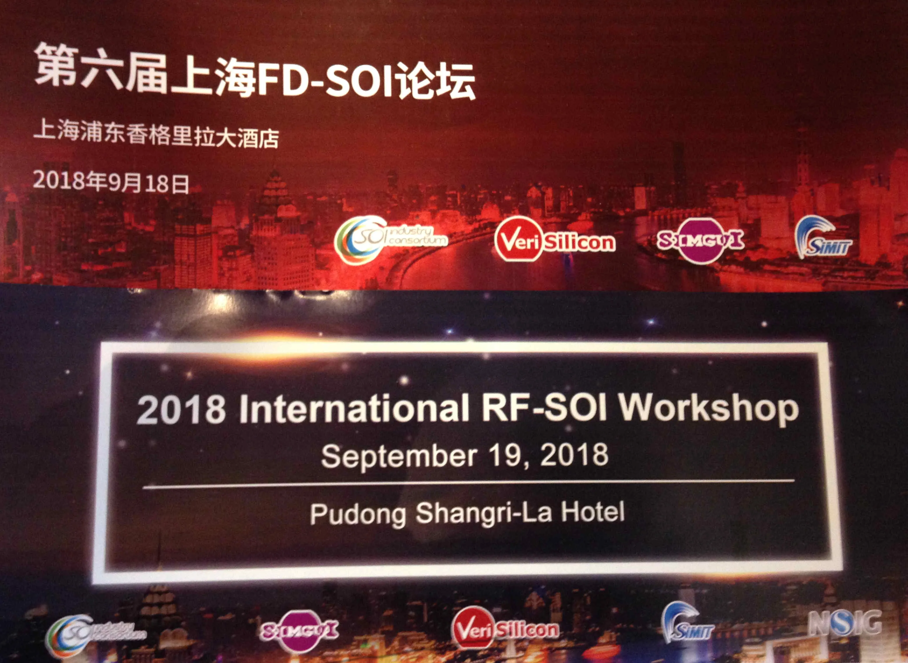
Excellent news and exciting applications made headlines at the recent FD-SOI and RF-SOI events in Shanghai. During the FD-SOI day, Amazon/Blink and Intellifusion shared news about their new chips, and we got updates from GF and Samsung. The RF-SOI day featured a great talk with details about China Mobile's 5G plans, and peeks at Nokia's groundbreaking approach and Qorvo's outlook. [caption id="attachment_12354" align="alignright" width="300"] (Photo courtesy: Verisilicon)[/caption] The hall was absolutely full – with over 300 people attending each day. The FD-SOI event was by invitation only, and there were far more people wanting to attend than there was room for, even given the big room in which the events were held. The events got excellent coverage in the China tech press. For example, EEWorld started with an overview article and added five supporting pieces zooming in on key presentations and companies: one on GlobalFoundries, one on Samsung, one on Verisilicon, and two on Soitec (CEO and top exec interviews). These pieces are in Chinese, but just open the links through your favorite translation site. Many of the key slides are captured in these articles, so if you can't wait for the ppts to be posted on the SOI Consortium website, you can get some quick previews now. The Verisilicon PR folks also wrote up highlights of the FD-SOI event in real time with lots of great pictures – you can read that here. Many thanks to that team, too, for flagging the coverage in the China press and posting it on their WeChat account. On the RF-SOI side, the Simgui folks wrote that up – you can read it here. They also sponsored a gala dinner with awards given to Qorvo and SmarterMicro – you can read about that here. Most of the presentations will be posted on the SOI Consortium website over the next few weeks, at which point we'll cover them in-depth here at ASN. But for now, here's a quick round-up of some of the highlights. FD-SOI Highlights [caption id="attachment_12347" align="alignright" width="300"] (Courtesy: Blink, Verisilicon)[/caption] Boston-area based Blink, which makes very popular home security systems, was recently bought by Amazon (see their current product page here). They just taped out a new chip on Samsung's 28FDS FD-SOI technology, and they're really happy about it. “I believe for battery powered devices at home, FD-SOI is the way to go,” said Yantoa Jia, Head of ASIC China Ops at Blink. Their goal in the move from 55nm bulk to 28nm FD-SOI was to double battery life, add features and control costs: and they did it. Even adding two more CPU cores and lots more features, “The power drop is fantastic,” he said. Design was no problem, he continued, and there was plenty of IP. Once the new generation is officially announced, he promised to sit down with ASN and give us more details. Attendees also heard about a new chipset from Intellifusion, which is putting its face recognition technology onto GlobalFoundries' 22FDX FD-SOI with design house Verisilicon. CEO Nin Chen gave an impromptu talk about how their technology is used to find missing people and property. The new chip, which is especially designed for use in cities, is network-to-cloud leveraging AI. For his part Thomas Morgenstern, GlobalFoundries SVP and GM of the Dresden Fab 1, said they're seeing high yields and increasing capacity for 22FDX. The marketing and manufacturing ecosystem has been built around the fab in Europe. Now, he said, the key is to build an FD-SOI ecosystem in China. The market needs of China largely parallel those of Europe, he noted, for performance and efficiency at the right cost point. The ecosystem enables fast time-to-market and 1st-time-right. [caption id="attachment_12343" align="alignleft" width="300"] (Photo courtesy: Cadence)[/caption] Samsung SVP Gitae Jeong sees their FD-SOI technology as the right solution for the 4th Revolution, which includes everything from energy harvesting to self-driving cars. They've just taped out their first 5G mmWave cellular chip on 28FDS, he revealed. eMRAM is looking very good, only requiring three additional masks and getting stable yields from -40o to 105oC. 18FDS is on schedule, with PDK 0.5 now being released, and 1.0 on track for release in March 2019. They expect a very fast ramp, and are looking at a 35% area reduction, power cut in half and performance up 22% compared to 28FDS. RF-SOI Highlights [caption id="attachment_12350" align="alignright" width="300"] China Mobile, Project Manager Danni Song (Photo courtesy: Simgui)[/caption] When China Mobile talks, the world listens. Project Manager Danni Song presented again this year (she gave a great talk last year, too). China has a very ambitious 5G project underway, and under two years in which to roll it out. The biggest challenges are power consumption and cost (a problem made worse by the additional power amplifiers needed for MIMO). Can RF-SOI help solve these challenges, she asked? One thing she did clarify during the panel discussion was with respect to the mmWave part of the 5G puzzle. Their initial 2020 rollout will only focus on sub-6GHz, with mmWave following a year or two later. Michael Reiha, Head of RFIC R D at Nokia Mobile Networks clarified the worldwide 5G rollout during the panel discussion. Different locations on the planet have different histories and needs, so will rollout 5G in different ways. For historical reasons (and a lack of choice), the US will lead with mmWave, he said. Europe, meanwhile, will focus on 24GHz to meet the needs of automotive radar. In his presentation, Reiha described Nokia's approach to power amplifiers (PA), which is very different from what others are doing. With RF-SOI, he said, you can add sensors and logic for a level of preventative care, so you can gauge and protect your equipment using AI. He believes this disruptive approach will put them two years ahead of the industry, enabling massive MIMO to be deployed in dense urban areas with 60% lower power consumption and 50% savings in material costs. Go read about their Reefshark tech, he urged, which he says will beat GaAs. “The future is very bright with RF-SOI,” he concluded. “I can state that with confidence.” [caption id="attachment_12351" align="alignleft" width="300"] Julio Costa, Director of Technology Development, Qorvo (Photo courtesy: Simgui)[/caption] Julio Costa, Director of Technology Development at Qorvo sees it differently. Traditionally a GaAs house, all their RF-SOI work is fabless. While RF front end modules (FEMs) are loaded with RF-SOI, he said, and are a big winner for antenna tuning, Qorvo still sees GaAs for high-efficiency amplifiers and envelope tracking. But, he said, it will be a battle. GaAs wins in terms of area and power consumption he contends, but adds that SOI wins in terms of cost. Power levels, he predicts, will be the determining factor. So that's the quick overview – we'll drill down into the presentations as they're posted, so stay tuned!
Read More
Outsourced Semiconductor Assembly and Test (OSAT) service providers experienced strong growth in 2017, but will this growth continue? In the last few years, OSAT growth has been driven by shipments for packages found in smartphones, but this market is slowing. What will replace it? Growth in power devices is strong and electronic content in vehicles is increasing. Will OSATs participate in this growth? Many OSATs have plants dedicated to automotive package assembly and will see continued growth. Growing demand for connectivity everywhere, called IoT, is generating large amounts of data, creating the need for more servers and datacenters. The adoption of Artificial Intelligence (AI) across a broad range of applications is driving demand for high-performance packages, but will this assembly take place at the OSATs or foundries? In the third and fourth quarters of 2017, growth in cryptocurrency provided unanticipated revenue for a number of OSATs. Given that the most well-known crypto mining companies and the biggest mining pools are all based in China, several OSATs, including major Taiwanese and Chinese service providers, experienced revenue growth in 2017 directly attributed to the assembly of ASICs in flip chip scale packages (FC-CSPs) and GPUs in flip chip ball grid arrays (FC-BGAs) for the cryptocurrency market. However, the first and second quarter of this year has seen decreased demand for GPUs and ASICs for this application. The assembly of packages for cryptocurrency slowed considerably in the first half of the year and therefore can’t be counted on to add as much to the revenue base as in the previous year. Going into the latter half of the year, the demand for Crypto ASICs is expected to pick up as new generation of 7nm chips will drive new investment and replacement cycle while crypto-mining GPU will see a further decline. Three of the top 10 OSATs, Jiangsu Changjiang Electronics Technology (JCET), Tianshui Huatian Technology (Huatian), and Tongfu Microelectronics (TFME), are based in China. China’s share of the top 10 OSATs’ revenue increased from slightly less than 23 percent in 2016 to more than 25 percent in 2017, and this trend is expected to continue. Crypto-related packaging and test business has certainly contributed a big portion of the share gain. Major OSATs such as TFME and Tianshui Huatian plan expansion in their plants and they expect to fill this added capacity in a broad range of packages. Huatian’s new Nanjing plant will include assembly for memory packages. TFME plans to set up a plant in Xiamen, Fujian Province to provide bumping, wafer level packaging, and system-in-packaging (SiP) services. Tracking the capabilities of OSATs is increasingly important. SEMI and TechSearch International have introduced a new Worldwide OSAT Manufacturing Site Database that provides listings of OSAT facility locations and package and test options in each factory. This database indicates the specific packages offered at each location. Finding plants that offer automotive qualified assembly is also possible with the database. Companies that offer bumping and wafer level packaging are identified. Over 120 companies and 300 facilities are tracked in this database covering both OSAT packaging and test facilities. For additional information about this informative database, please visit https://discover.semi.org/osat-database-registration.html E. Jan Vardaman is president of TechSearch International, Inc., and Clark Tseng is director of Industry Research and Statistics at SEMI.
Read More
U.S. Government Imposes Tariffs on $200 Billion of Goods and China Retaliates on $60 Billion of GoodsEarlier this week, the U.S. Trade Representative (USTR) released a 10 percent tariff on $200 billion in imports from China, including more than 90 tariff lines central to the semiconductor industry.The 10 percent tariff will take effect on September 24, 2018, and rise to 25 percent on January 1. These tariff lines will cost SEMI’s 400 U.S. members tens of millions of dollars annually in additional duties. However, counting the products included in the previous rounds of tariffs, the total estimated impact exceeds $700 million annually. China has already announced that it will respond with tariffs on $60 billion worth of U.S. goods. In his notice, President Trump said the U.S. will impose tariffs on $267 billion worth of goods if China retaliates. The U.S. government removed 279 total tariff lines, including three lines that impact our industry: silicon carbide, tungsten, and network hubs used in the manufacturing process.As we’ve noted, intellectual property is critical to the semiconductor industry, and SEMI strongly supports efforts to better protect valuable IP. However, we believe that these tariffs will ultimately do nothing to address the concerns with China’s trade practices. This sledgehammer approach will introduce significant uncertainty, impose greater costs, and potentially lead to a trade war. This undue harm will ultimately undercut our companies’ ability to sell overseas, which will only stifle innovation and curb U.S. technological leadership.Product Exclusion Process – List 2USTR formally published the details for the product exclusion process for products subject to the List 2 China 301 tariffs (the $16 billion tariff list). If your company’s products are subject to tariffs, you can request an exclusion.In evaluating product exclusion requests, the USTR will consider whether a product is available from a source outside of China, whether the additional duties would cause severe economic harm to the requestor or other U.S. interests, and whether the product is strategically important or related to Chinese industrial programs (such as “Made in China 2025”).The request period ends on December 18, 2018, and approved exclusions will be effective for one year, applying retroactively to August 23, 2018. Because exclusions will be made on a product basis, a particular exclusion will apply to all imports of the product, regardless of whether the importer filed a request.More information, including the process for submitting the product exclusion request and details what information should be included in your submission can be found here. Please let me know if your company plans on filing an exclusion. SEMI has prepared a document that includes guidelines for your exclusion filing, an explainer on how to submit, and links to official government info. SEMI is glad to assist your companies file exclusion requests for your products. SEMI will continue tracking ongoing trade developments. Any SEMI members with questions should contact Jay Chittooran, Public Policy Manager at SEMI, at [email protected].
Read More
SEMI Releases latest update to World Fab Forecast with adjusted semiconductor revenue consensus for second-half 2018 and 2019 Global semiconductor revenue in 2018 is now expected to reach $473.8 billion and clock a growth rate of 15 percent, a significant upward revision from the 7.5 percent expansion (to $442.9 billion) forecast at the start of the year by six research and investment forecasts tracked by SEMI Industry Research and Statistics (SEMI IR S). Data center growth will remain robust in the coming quarters, fueling demand for memory devices. In addition, cloud computing will continue to spur strong CPU, GPU, networking, ASIC, and DRAM and NAND demand through 2019, driving a consensus 3.63 percent year-to-year growth to reach the semiconductor revenue of $491 billion in 2019. Fab equipment spending (new and used) for 2018 is expected to increase by 14 percent to a record high of $63 billion, according to the last data from the SEMI World Fab Forecast, published by SEMI IR S. For 2019, fab equipment spending (new and used) is expected to increase 8 percent to another record of just under $68 billion. Memory continues to be the biggest swing factor in fab spending in 2018 and is expected to lead growth into 2020. 3D NAND will see the most capacity added in 2018 and 2019 with growth of 41 percent in 2018 and 27 percent in 2019, according to the SEMI World Fab Forecast. DRAM investment will see even stronger growth in 2018 and 2019 driven by new capacity addition as well as the continued technology shrink towards 1y/1z nm. For the first half of 2018, global spending for semiconductor fab equipment continues its growth momentum from 2017. Though we expect some softness in the second half of 2018, the outlook for 2019 remains robust with a fourth consecutive year of growth – the first such run since the 1990s. This prolonged growth cycle has been propelled by memory and will be extended by significant investment in China in 2019. Although a potential slowdown in 2020 is a concern, the overall outlook for semiconductor demand remains solid due to broad-based growth trends in data center, artificial intelligence (AI)/machine learning (ML), automotive, and industrial segments. Following are other SEMI forecasts for fab spending. Installed Capacity 3D NAND will see the most capacity added in both 2018 and 2019 with growth of 41 percent in 2018 and 27 percent in 2019. Foundry capacity growth is steady at 3 percent in 2018 and 6 percent in 2019, driven by both leading-edge and trailing-edge capacity buildup. 200mm fab capacity will increase 4 percent in 2018 and 3 percent in 2019, fueled by demand for MCU, sensors, PMIC, MOSFET and Driver IC. New Facilities / Construction Spending In 2018, there are 72 construction projects with investments totaling $15 billion, a year-over-year increase of 23 percent. Construction spending will reach all-time highs with China continuing its lead at US$7 billion in 2018, shattering its own record of $6.3 billion investment in 2017. Most construction spending in 2018 will be for Memory (just under $9 billion), primarily for 3D NAND followed by DRAM. Foundry will log second place in construction spending at just under $5 billion. Fab Equipment Spending Fab equipment spending (new and used) for 2018 is expected to jump 14 percent to a record high of US$63 billion, flat from the forecast issued in June 2018. Equipment spending (new and used) for 2019 is expected to increase 8 percent to another record of just under US$68 billion, a downward adjustment from +9 percent published in June 2018. We believe equipment spending will remain healthy, driven by solid, broad-based demand and predictable technology investments on top of constructive SEMICAP equipment fundamentals. Activity Report The August report features 1,265 records including about 300 Opto- and LED-related facilities. We have made 223 changes related to 216 fabs/lines. The modifications include the addition of new records, changes to existing records, the deletion of records since the February 2018 World Fab Forecast report. We are tracking 103 future facilities/lines with various probabilities that will start volume production in 2018 or later. Download a sample report Not a subscriber? Please review SEMI fab databases listed below. Our databases deliver the latest forecast and a complete analysis of front-end fabs and foundries worldwide. They are ideal resources to empower your market research. Eugenia Liu is a Senior Product Marketing Manager at SEMI.
Read More
The presentations from the SOI Consortium sponsored workshop held during Semicon West are now posted and freely available on the website – click here to see the full agenda with links to the presentations. The workshop, entitled 4G/5G Connectivity: Opportunities for the SOI Supply Chain, was well-attended and generated excellent discussions. If you don't have time to look at all of the ppts, here are quick overviews. Market Overview and FD SOI Opportunities, by Handel Jones, CEO, IBS. Handel Jones is an industry veteran, China expert and longtime follower of the SOI ecosystem. High performance with low power consumption are the key requirements for the continued growth in the semiconductor industry, he said, making FD-SOI the right choice for a wide range of products. Here's how he sees it: [caption id="attachment_12312" align="alignleft" width="300"] (Courtesy: IBS and SOI Consortium)[/caption] He estimates the yearly TAM (total available market) for FD-SOI based products in the range of $46 billion over the next 10 years, largely driven by needs for ultra-low power and RF integration. He goes on to break out volumes by applications (including ISPs – image signal processors; and CIS – CMOS image sensors), foundry markets by feature dimension and to map out technology trends. Mobile Radio Transformation in the Age of 5G: A Perspective on Opportunities for SOI, Peter Rabbeni, Vice President, Globalfoundries. Peter Rabbeni is an RF expert par excellence, having overseen the shipping of over 35 billion RF-SOI products to date. In his presentation, he details how 5G NR (New Radio) sub-6GHz frequency band specifications significantly increase frequency range and channel bandwidth, and how new band support and MIMO complexity and die size per handset are driving complexity in RF FEMs. Furthermore, 5G/mmWave phased arrays are driving a paradigm shift in the approaches that can be taken, he explains, so greater integration is needed. Here's a great slide showing where GF's two main SOI technologies come into play: [caption id="attachment_12311" align="alignleft" width="1000"] (Courtesy: GlobalFoundries and SOI Consortium)[/caption] Empowerment of 5G with SOI-Based Technologies, Emmanuel Sabonnadière, CEO, Leti-CEA. [caption id="attachment_12310" align="alignleft" width="300"] (Courtesy: Leti and SOI Consortium)[/caption] Working in partnership with industry leaders around the world, Leti has been the research powerhouse behind all things SOI since the early 1980s. In fact Reuters ranks them #2 in their most recent list of the World’s Most Innovative Research Institutions. This presentation reviews the key technical benefits of FD-SOI for IoT and IMT (that's international mobile communications, btw). Engineered Substrates – at the Foundation of 5G, Thomas Piliszczuk, Executive Vice President, Soitec. This presentation really puts the context around engineered substrates. Here are two excellent and useful slides here that identify which engineered substrates go where in the 5G world, and the engineered substrates that Soitec provides. Check these out: [caption id="attachment_12309" align="alignleft" width="1000"] (Courtesy: Soitec and SOI Consortium)[/caption] [caption id="attachment_12308" align="alignleft" width="1000"] (Courtesy: Soitec and SOI Consortium)[/caption] Ultra-thin Double Layer Metrology with High Lateral Resolution, Bernd Srocka, Vice President, Unity GmbH. [caption id="attachment_12307" align="alignleft" width="300"] (Courtesy: Unity and SOI Consortium)[/caption] In case you're not familiar with them, Unity provides a wide range of solutions in metrology and inspection. Both the top silicon layer and BOX layer of wafers for FD-SOI applications have draconian requirements that have required new approaches in metrology to ensure the thickness and homegeneity control of these very thin layers. China 5G Plan and SOI Ecosystem, Jeffrey Wang, CEO, Simgui. Shanghai-based Simgui partners with Soitec, using SmartCut™ technology for the production of RF-SOI wafers. It is doubling its capacity to reach 400K over the next year, and expanding into 300mm. China is aggressively working on 5G and plans to deploy 5G commercialization in 2020. Jeff Wang's is a terrific presentation detailing the rollout. (BTW, in addition to the massive funding effort underway, the government created the National Silicon Industry Group (NSIG) to support the semiconductor material ecosystem in China. You'll want to keep up with what's going on here). Here's the slide that summarizes the SOI ecosystem in China – the presentation then goes on to detail who does what. [caption id="attachment_12306" align="alignleft" width="1000"] (Courtesy: Simgui and SOI Consortium)[/caption] Inspection and Metrology Relevance in SOI Manufacturing, Jijen Vazhaeparambil, Vice President General Manager, KLA-Tencor. [caption id="attachment_12305" align="alignleft" width="300"] (Courtesy: KLA-Tencor and SOI Consortium)[/caption] K-T has played a strategic role in the SOI story going back for decades (and in fact they wrote a piece for the third edition of ASN back in 2005!), ensuring metrology innovations for things that hadn't previously need detection and measurement. With each new set of requirements, they rose to the occasion with wafer metrology solutions that helped increase quality and decrease costs. This presentation recaps some of them.
Read More
The China IC Ecosystem Report, a comprehensive report for the IC manufacturing supply chain, reveals that front-end fab capacity in China will grow to account for 16 percent of the world's semiconductor fab capacity this year, a share that will increase to 20 percent by the end of 2020. With the rapid growth, China will top the rest of the world in fab investment in 2020 with more than $20 billion in spending, driven by memory and foundry projects funded by both multinational and domestic companies, according to the new report released today by SEMI.The report also shows that IC Design remained the largest semiconductor sector in China for the second year in a row with $31.9 billion in revenue in 2017, widening its lead over the long-dominant IC Packaging and Test sector. The ascent of China’s IC Design sector comes as the region’s equipment market is expected to claim the top spot in 2020 for the first time on the strength of the continuing development of its domestic manufacturing capability. China’s maturing domestic fab sector is also benefiting domestic equipment and materials suppliers. Both groups continue to see gains in their product offerings and capabilities, particularly in silicon wafer production. The China IC Ecosystem Report is produced by SEMI, the global industry association and provider of independent electronics market research.The more than RMB140 billion (US$21.5 billion) accumulated by the National IC Fund, a critical component of the 2014 National Guideline to address China’s semiconductor trade deficit, has spurred rapid gains throughout the region’s IC supply chain. Semiconductors are China’s largest import by revenue. Phase 2 of funding aims to raise another RMB150-200 billion ($23.0-$30.0 billion).Encouraged by the National Guideline and favorable policies, skilled overseas talent is returning to China, triggering an explosion of domestic IC Design start-ups that are benefiting from access to investment and favorable policies, the report shows.Other highlights from The China IC Ecosystem Report include: Currently 25 new fab construction projects are underway or planned in China. 17 - 300 mm fabs are being tracked as part of this investment and expansion activity. Foundry, DRAM and 3D NAND are the leading segments for fab investment and new capacity in China. China’s IC Packaging and Test industry is also moving up the value chain by enhancing its technology offerings through mergers and acquisitions and building advanced capabilities to entice international integrated device manufacturers. China’s IC materials market, currently dominated by Packaging materials, became the second largest regional market for materials in 2016, a position it solidified in 2017. China’s materials market is expected to grow at a 10 percent CAGR from 2015 to 2019, driven primarily by the region’s new fab capacity ramp in the coming years. Fab capacity will expand at a 14 percent CAGR during that period. The China IC Ecosystem Report covers the latest semiconductor supply chain and market developments including the rise of China’s IC industry, national and local government policies, public and private funding, and their implications for China's IC supply chain. The report also compares key domestic companies and their international peers segment by segment. To learn more and get a sample of the report, visit http://www.semi.org/en/china-ic-ecosystem-report.Eugenia is a Senior Product Marketing Manager at SEMI.
Read More
In testimony today before a U.S. government interagency panel considering tariffs on $200 billion worth of Chinese goods, SEMI called for the removal of nearly 100 tariff lines, all of which cover items critical to the semiconductor manufacturing process, including materials and machines.Jonathan Davis, global vice president of advocacy at SEMI, explained in his testimony that while SEMI strongly supports efforts to better protect valuable intellectual property (IP), tariffs will not help address Chinese trade practices, and will ultimately have significant and unintended consequences. SEMI asserts that these tariffs will harm companies in the semiconductor supply chain by increasing business costs, introducing uncertainty, and stifling innovation. Collectively, SEMI estimates that this round of tariffs will cost its 400 U.S. members more than tens of millions annually in additional duties. All told, SEMI estimates that all U.S. and Chinese retaliatory tariffs will cost members nearly $700 million in annual duties. SEMI’s full written comments note that these tariffs, on top of those already in force and the retaliatory tariffs, will hamstring the industry. The tariffs seem to target U.S. firms for simply operating in China. Given that tools and materials are extremely complex, precise, and difficult to manufacture, it is unreasonable to believe that a constituent component can simply be replaced with a part from another source. Further, this U.S. government approach does not take into account that many items subject to these tariffs are not available, at sufficient quality and cost, from domestic sources, or even non-Chinese sources. We stand steadfast in our belief that this trade action will raise prices, put thousands of high-paying and high skill jobs at risk, and curb growth.Over the past four months, SEMI submitted written comments and offered testimony on the two previous rounds of tariffs, citing the damaging impact tariffs would have on the U.S. semiconductor industry. The first round of tariffs – on $34 billion worth of Chinese goods – took effect July 6, and the second round – targeting $16 billion in Chinese imports – will be imposed on August 23. The tariffs hit machines and tools central to the semiconductor industry, including equipment used to manufacture wafers, boules, and chips as well as test, inspection and sensing equipment. We urge SEMI members to review the $200 billion U.S. tariff list to determine the level, if any, of impact. We also strongly encourage members to review Chinese retaliatory lists as well. Any SEMI members with questions should contact Jay Chittooran, Public Policy Manager at SEMI, at [email protected].
Read More