downloadGroupGroupnoun_press release_995423_000000 copyGroupnoun_Feed_96767_000000Group 19noun_pictures_1817522_000000Member company iconResource item iconStore item iconGroup 19Group 19noun_Photo_2085192_000000 Copynoun_presentation_2096081_000000Group 19Group Copy 7noun_webinar_692730_000000Path
Skip to main content
Default Banner Image

Smart Manufacturing

read more

The SEMI Smart Manufacturing Initiative collaboratively crafted this whitepaper with industry members to offer insights from a recent workshop, presenting a comprehensive view of Digital Twin technology in semiconductor manufacturing for achieving AI-driven autonomous factories, covering industry definitions, taxonomy descriptions, and challenges in development and deployment.

Smart Manufacturing White Paper English
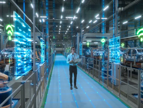
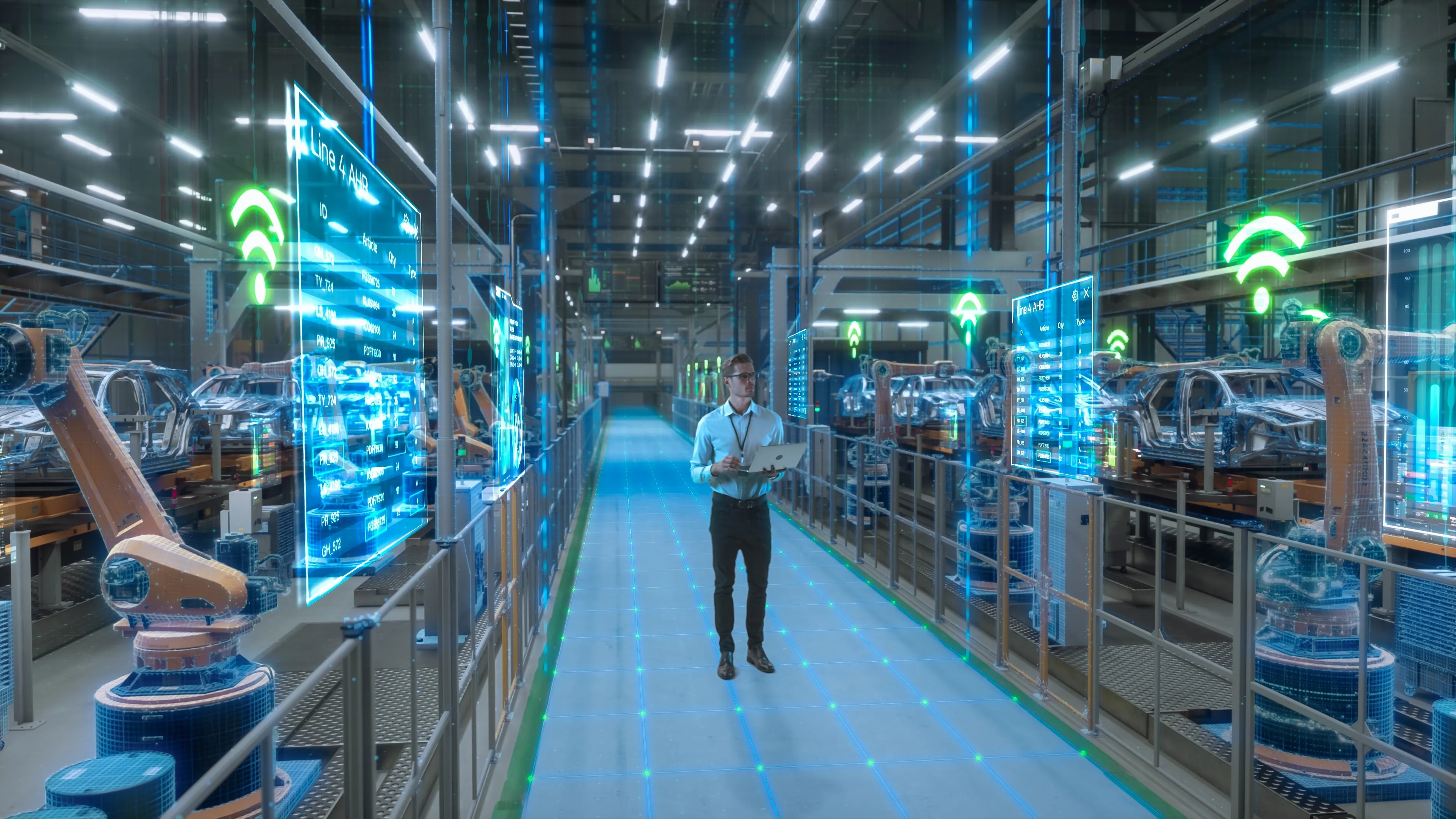
The semiconductor industry is hitting a structural inflection point: explosive AI‑driven demand, rapidly rising manufacturing complexity, and stringent sustainability expectations are converging at once. In this context, edge AI deployed directly on tools, sensors, and local controllers, is shifting from experimental to essential, particularly in fabs where milliseconds matter. SEMI’s timely workshop, Smarter Sensors, Smarter Fabs: AI at the Edge in Semiconductor Manufacturing, taking place March 18–19, 2026 in Milpitas, CA, will address this important topic.From sparse sensing to dense instrumentationTwo decades ago, most process tools relied on dozens of sensors per chamber. Today, leading etch, deposition, CMP, and lithography systems routinely integrate hundreds of sensing channels spanning pressure, flow, RF power, optical endpoint, vibration, and chemistry. At 3 nm and 2 nm, process windows are so tight that yield hinges on multivariate understanding of chamber conditions and tool state rather than a few independent alarms. Sensor proliferation has turned fabs into rich data environments—but also exposed the limits of traditional, centrally managed control.Why edge AI is displacing cloud‑only controlConventional architectures push heavy analytics to centralized servers or the cloud, with supervisory systems periodically updating recipes, setpoints, or dispatch rules. Across manufacturing, measured cloud round‑trip times commonly range from 800 to 2,400 ms, whereas edge systems co-located with equipment can respond in 15–45 ms, roughly 50–160× faster. For safety‑ and yield‑critical loops in semiconductor manufacturing, that latency gap is often unacceptable.At the same time, new generations of low‑power neural processing units (NPUs) and edge accelerators deliver tens of trillions of operations per second (TOPS) at single‑digit watt budgets, making always‑on inference viable inside tools, cameras, and controllers. The result is a decisive move toward edge‑native architectures: models execute where data is produced, while cloud resources are reserved for retraining and fleet‑wide learning.Edge AI on the line: control, inspection, and maintenanceIn process control, edge AI is enabling a shift from univariate threshold checks to multivariate models that understand the joint dynamics of sensor streams. Platforms today embed deep‑learning and statistical models directly at or near the tool, performing real‑time endpoint prediction and anomaly detection from high‑dimensional time series. Similar approaches are emerging in lithography and CMP, where local inference helps keep focus, overlay, and removal rate within spec before wafers drift out of control.Inspection and logistics are undergoing a similar transformation. Vision systems with embedded NPUs classify defects at line speed, often above 100 parts per minute, eliminating the need to ship large image volumes to a central cluster. Robots and autonomous mobile robots (AMRs) use local intelligence for short‑horizon planning and collision avoidance, while higher‑level systems focus on global scheduling and optimization.Predictive maintenance is one of the most mature applications: vibration, acoustic, temperature, and pressure data are analyzed locally to detect anomaly signatures hours or days before conventional thresholds trip. Reported benefits include reductions in unplanned downtime, longer component life, and lower maintenance costs when these models are integrated into manufacturing execution systems (MES) and maintenance workflows.Digital twins and agentic AI on top of edge dataDigital twins build on this sensing and edge‑analytics foundation. By maintaining virtual, live‑updated models of tools, lines, and entire fabs, they enable scenario testing, debottlenecking, and root‑cause analysis without putting WIP at risk. Vendors and early adopters report that such twins can shorten process‑node ramps and facility bring‑up by enabling thousands of “what‑if” experiments before physical changes are made.​Agentic AI is now emerging as the orchestration layer above these twins. In semiconductor case studies, agents connected to MES, advanced process control (APC), and planning systems have delivered double‑digit improvements in throughput, cycle time, and tool utilization by autonomously adjusting routing, batch sizes, and scheduling in response to live fab conditions. Other agents mine unstructured engineering notes and fault reports to accelerate root‑cause analysis, turning hard‑won lessons into repeatable, codified behavior.Sustainability as a first‑class requirementSustainability pressures are reinforcing this stack. Semiconductor manufacturing is energy‑ and resource‑intensive, and regulators and customers alike are demanding more transparency and improvement. Edge‑connected monitoring of energy, utilities, and emissions has already helped some fabs cut energy‑related costs by around 20 percent through tighter control of HVAC, process gases, and idle modes. Research initiatives such as imec’s Sustainable Semiconductor Technologies and Systems (SSTS) program are using virtual fab methods and detailed life‑cycle assessment to guide process and equipment choices for lower environmental impact.Strategic takeaways and where to learn moreThe trajectory is clear: fabs that combine dense sensing, edge AI, digital twins, and agentic AI are building toward continuously learning, self‑optimizing operations. Architectures will need to be edge‑first rather than cloud‑only. Simply adding sensors without local intelligence will not deliver competitive advantage, and environmental KPIs are likely to be optimized with the same rigor as yield and cycle time.For practitioners who want to translate these trends into roadmaps, the Smarter Sensors, Smarter Fabs: AI at the Edge in Semiconductor Manufacturing” workshop (March 18–19, 2026, Milpitas, CA) spearheaded by the SEMI Manufacturing Coalitions* will bring together experts in sensing, edge architectures, digital twins, and agentic AI to share concrete deployments and architectures tailored to semiconductor fabs.*The SEMI Manufacturing Coalitions include Smart Manufacturing, Fab Owners Alliance (FOA) MEMS and Sensors Industry Group (MSIG), Advanced Packaging Heterogenous Integration (APHI) and Semiconductor Components, Instruments, and Subsystems (SCIS). Anshu Bahadur is Senior Program Manager, Technology Communities at SEMI. Mark da Silva is Senior Director, Manufacturing Coalitions at SEMI.
Read More
In recent years, SEMI has been increasing its attention to sustainability within the global semiconductor industry. With the formation of the Semiconductor Climate Consortium (SCC) within the SEMI Sustainability Initiative, member companies have joined hands to collaborate and collectively tackle the challenge of meeting the industry’s ambitious sustainability goals.The SEMI Smart Manufacturing Initiative is a global effort focused on the future of manufacturing in electronics that helps microelectronics manufacturers enable business value by facilitating awareness and problem-solving to reduce barriers and realize timely ROI for critical Industry 4.0/5.0 technology deployment.Addressing the Industry’s Sustainability Inflection Point The Initiative’s Accelerating Sustainability with Smart Manufacturing Task Force formed in the summer of 2023 is a pivotal effort that collaborates with the SEMI Sustainability Initiative. The task force provides the “how” to the “what” of corporate sustainability goals, focusing on a bottom-up approach that leverages various sensing technologies, at the cleanroom, sub-fab and facilities levels for both greenfield and brownfield device-making facilities, to enable predictive analytics.The task force is designed to be a driving force to encourage the industry’s shift from a fragmented, top-down approach – which does not address the increasing usage of carbon as device-making becomes more complex – to a more integrated, bottom-up strategy. The task force has created a roadmap based on three pillars comprising connecting, sensing, and predicting technologies, which are meant to be cumulative and could dramatically reduce the carbon footprint for making microelectronics like semiconductors. The task force participants believe this to be the first industry roadmap to address all areas of fab processing, leveraging Industry 4.0/5.0, including AI for the purpose of enhancing the sustainability of operations.The task force’s roadmap is comprehensive and includes a variety of sensing technologies, digital twin methodologies, and machine learning/AI techniques for reducing Scope 1 (direct, process-based) and Scope 2 (indirect, energy-related) greenhouse gas (GHG) emissions, water usage and material waste. Once the roadmap is completed, factory management can prioritize the implementation of best practices based on the quantified impact factors of specified use cases. The roadmap outlines methodologies for brownfield and greenfield fabs separately based on practical capex and implementation recommendations.The task force has finalized its assessment of practical solutions for reducing Scope 1 and Scope 2 emissions, and it is now addressing water usage best practices before addressing material waste later this year and into 2025. SEMI will publish separate white papers regarding Scope 1 and 2 as a precursor to offering the roadmap as a customized tool for fabs.The semiconductor manufacturing industry stands at an inflection point from a sustainability perspective. Consider this: U.S. CHIPS Act funding is set to support 19 greenfield fabs, which collectively will consume the equivalent of 11 Empire State Buildings’ worth of steel. That’s a monumental environmental impact. Additionally, the Q2 2024 SEMI World Fab Forecast is tracking approximately 104 new fabs worldwide coming online between 2023 and 2027. Each of these fabs requires significant amounts of concrete, steel, and construction equipment, all with their own GHG footprints. This all represents a challenge that the industry must grapple with head-on.Furthermore, there is the energy-intensive nature of large semiconductor fabs, the cost implications of renewable power acquisition, and the substantial water usage by medium and mega-sized fabs. The main mission of the task force is to create an industry roadmap—a practical blueprint—for device makers to invest in sustainability, following a systematic, bottom-up approach.Accelerating Sustainability with Smart Manufacturing at SEMICON West At the Smart Manufacturing Pavilion at SEMICON WEST 2024 , a special session centered around the key components of the Accelerating Sustainability with Smart Manufacturing Task Force roadmap. Task force leaders helped coordinate a unique session to showcase the roadmap findings and detailed case studies for Scope 1 and 2 emissions. The session included speakers from Deloitte, Linkan Engineering, Micron, Solvay, Spectrum Environmental Services, and ULVAC.Accelerating Sustainability with Smart Manufacturing Session at SEMICON West 2024The opening keynote by Adeline Tay of Micron covered the company’s pioneering efforts to improve sustainability in semiconductor manufacturing. Tay highlighted how to enable a net-zero transition sooner via smart manufacturing technologies including digital twins, real-time power monitoring and optimization, lower global warming potential gas usage, and emission data visibility.The next presentation by Brian Coppa (Task Force Co-Chair) of ULVAC [1] revealed the findings of the SEMI task force roadmap, which described the most critical technologies to reduce Scope 1 and 2 emissions and quantified them with respect to impact level to help fab managers prioritize budget allocation for meeting related sustainability goals at the cleanroom, sub-fab and facilities levels. Coppa provided estimates on the substantial decreases in emissions that can be achieved (see Figure 1) using the compilation of recommended technologies (i.e. predictive analytics such as AI, machine learning and predictive maintenance) that are outlined in the task force roadmap. Figure 1: Task force roadmap estimates for the emissions reduction potential for Scope 1 and 2, respectively.Jake Townsend of Deloitte [2] followed and underlined the industry’s sustainability challenge with regards to chip-making carbon footprint and the opportunities from design to fab, to sub-fab and facilities. Townsend presented that the industry’s water management carbon footprint is estimated to be at least 2 orders of magnitude higher by weight compared to consumer products such as a car or hamburger.Next, Steve Hall of Spectrum Environmental Solutions [3] discussed how compliance testing and measurements differ from common GHG reporting, which is calculation based. The Electronics Code for Federal Regulations 40CFR 98 Subpart 1 now requires the electronics industry to report both calculated emission factors and smokestack measurements. Hall showed the benefits of Fourier-transform infrared spectroscopy (FTIR) monitoring at the smokestack level and the accuracy it can provide for reporting.Michael Peter Pitroff of Solvay [4] provided an in-depth case study on how the F2-based cleaning gas Solvaclean® can replace SF6 chemistries for chamber cleans, facilitated by in-situ gas monitoring techniques, to reduce Scope 1 emissions in plasma etch and deposition processes. Pitroff covered the financial and throughput impacts of the replacement and described how higher global warming potential (GWP) gases can be replaced with low GWP gases in Bosch wafer etch processes.Finally, Drew Horseman of Linkan Engineering [5] presented innovations in water treatment for the semiconductor industry. Horseman covered current state-of-the-art, energy-efficient reverse osmosis (RO) systems and addressed specific benefits of RO optimization. He showed how data acquisition and analytics are the first step to eventually reaching zero-liquid-discharge (ZLD), which is the future of sustainable water treatment.Get Involved!Overall, the Smart Sustainability session at the Smart Manufacturing Pavilion at SEMICON West 2024 enlightened many attendees on how smart manufacturing technologies like AI can help advance sustainability in semiconductor manufacturing using a more scalable, automated approach. Visit the SEMI Smart Manufacturing Initiative homepage to learn more about upcoming activities and contact [email protected] to get involved in the task force.Amit Srivastava is Manager, Data Science- Smart Manufacturing and Artificial Intelligence at Micron Technology, Brian Coppa is Product Engineering Lead at ULVAC, and they lead the SEMI Accelerating Sustainability with Smart Manufacturing Task Force. Mark da Silva is Senior Director of the Smart Manufacturing Initiative and APHI Technology Community at SEMI. Topics: Smart Manufacturing , SEMI Smart Manufacturing Initiative , semiconductor manufacturing , Digital Twin standards , manufacturing productivity , Digital Twin framework , manufacturing efficiency , semiconductor industry , semiconductor ecosystem, sustainability , SEMICON West , decarbonization , Semiconductor Climate Consortium , greenhouse gas emissionsReferences from the Smart Sustainability Session at Smart Manufacturing Pavilion available to SEMICON West 2024 attendees: SEMI Smart Sustainability Roadmap: Blueprint for Device MakersGreen Chips are the New Blue-Chip InvestmentMeeting Net Zero Manufacturing Challenges with Real-Time Monitoring of Exhaust Laterals in Sub-FabsSolvaClean as replacement of SF6 in cleaning and etchingInnovations in Water Treatment: Exhibiting the Importance of Data in Sustainable Process Development
Read More