downloadGroupGroupnoun_press release_995423_000000 copyGroupnoun_Feed_96767_000000Group 19noun_pictures_1817522_000000Member company iconResource item iconStore item iconGroup 19Group 19noun_Photo_2085192_000000 Copynoun_presentation_2096081_000000Group 19Group Copy 7noun_webinar_692730_000000Path
Skip to main content
Default Banner Image

Business and Markets

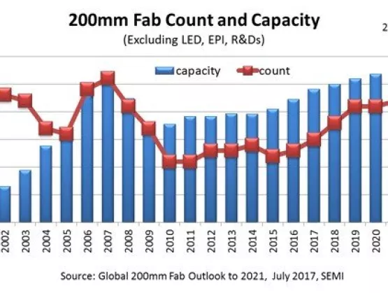
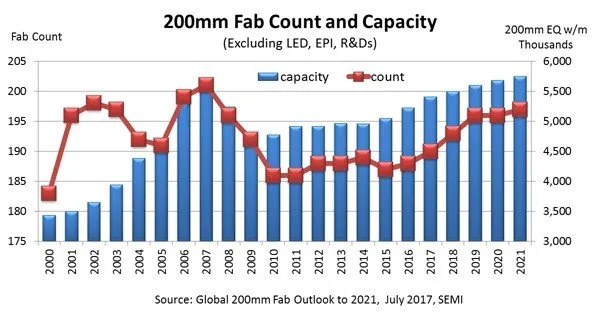
In the shadow of other more trendy news about China and Memory fab investments, 200mm fabs continue to “flex their muscles.” At least 500,000 wafers per month (wpm) capacity, or a 10 percent expansion, is forecast for 200mm fabs from this year through 2021. This includes capacity from a number of new 200mm fabs expected to start operation in 2017. The recently published report "Global 200mm Fab Outlook to 2021" by SEMI is tracking production, pilot, and R D 200mm facilities worldwide with a special focus on capacity expansions and new facilities. Driven by mobile and wireless applications, IOT, and automotive, the 200mm market is thriving. Many of the products used in these applications are produced on 200mm wafers, so companies are expanding capacity in their facilities to the limit, and there are nine new 200mm facilities in the pipeline. Looking only at IC volume fabs, the report shows 188 fabs in production in 2016 and expanding to 197 fabs by 2021. China will add most of the 200mm capacity through 2021, with 34 percent growth rate from 2017 to 2021, followed by South East Asia with 29 percent and the Americas with 12 percent. SEMI’s recent publication of the “Global 200mm Fab Outlook report to 2021” (July 2017) is the third update since the report was first launched in 2015. Since the last release in November 2016, the SEMI Industry Research and Statistics analyst team has made 232 changes and updates to 132 fabs. The report tracks over 300 facilities using 200mm wafers from R D, EPI, LED fabs to volume IC fabs. For more information, visit: https://discover.semi.org/global-200mm-fab-outlook-registration.html
Read More
SEMI reported that worldwide sales of new semiconductor manufacturing equipment are projected to increase 19.8 percent to total $49.4 billion in 2017, marking the first time that the semiconductor equipment market has exceeded the market high of $47.7 billion set in 2000. In 2018, 7.7 percent growth is expected, resulting in another record-breaking year ─ totaling $53.2 billion for the global semiconductor equipment market. The SEMI Mid-year Forecast predicts wafer processing equipment is anticipated to increase 21.7 percent in 2017 to total $39.8 billion. The other front-end segment, which consists of fab facilities equipment, wafer manufacturing, and mask/reticle equipment, will increase 25.6 percent to total $2.3 billion. The assembly and packaging equipment segment is projected to grow by 12.8 percent to $3.4 billion in 2017 while semiconductor test equipment is forecast to increase by 6.4 percent, to a total of $3.9 billion this year. In 2017, South Korea will be the largest equipment market for the first time. After maintaining the top spot for five years, Taiwan will place second, while China will come in third. All regions tracked will experience growth, with the exception of Rest of World (primarily Southeast Asia). South Korea will lead in growth with 68.7 percent, followed by Europe at 58.6 percent, and North America at 16.3 percent. SEMI forecasts that in 2018, equipment sales in China will climb the most, 61.4 percent, to a total of $11.0 billion, following 5.9 percent growth in 2017. In 2018, South Korea, Taiwan, and China are forecast to remain the top three markets, with South Korea maintaining the top spot to total $13.4 billion. China is forecasted to become the second largest market at $11.0 billion, while equipment sales to Taiwan are expected to reach $10.9 billion. The following results are in terms of market size in billions of U.S. dollars: The Equipment Market Data Subscription (EMDS) from SEMI provides comprehensive market data for the global semiconductor equipment market. A subscription includes three reports: the monthly SEMI Billings Report, which offers an early perspective of the trends in the equipment market; the monthly Worldwide Semiconductor Equipment Market Statistics (SEMS), a detailed report of semiconductor equipment bookings and billings for seven regions and over 22 market segments; and the SEMI Mid-year Forecast, which provides an outlook for the semiconductor equipment market. For more information or to subscribe, please contact SEMI customer service at 1.877.746.7788 (toll free in the U.S.). For more information online, visit: https://discover.semi.org/equipment-market-data-registration.html
Read More
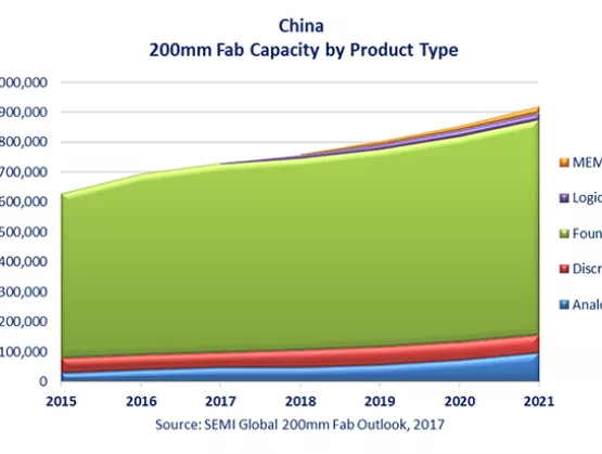
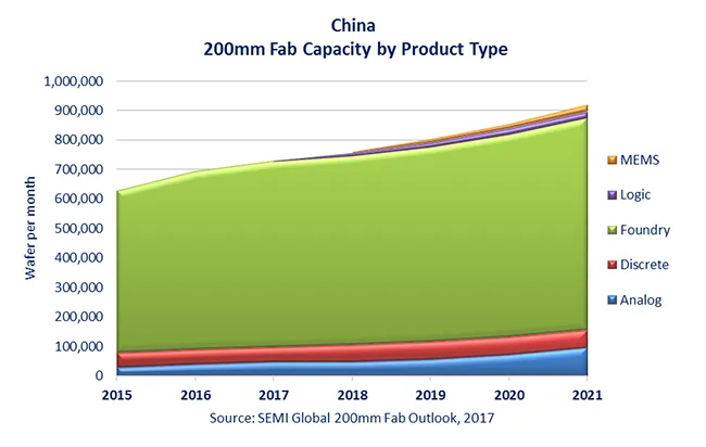
By Clark Tseng, Industry Research Statistics Group, SEMI China’s ambitious plans to build a world-class semiconductor manufacturing supply chain domestically certainly has the industry’s attention. With over a dozen new 300mm fab announcements lately from Foundries, DRAM, 3D NAND, and as well as CMOS image sensor companies (either from international semiconductor makers or from indigenous players), China has launched a huge investment in wafer fab capacity that is expected to ramp in the next five years. While advanced 300mm fab investment attracts most of the attention and resources, China does not skimp on the more “matured” 200mm fabs. China will have the most new 200mm fab projects and capacity additions in the next few years compared to other regions. According to SEMI’s latest 200mm Fab Outlook report, China currently has about 700,000 wafers per month (wpm) installed fab capacity, and this is forecasted to surpass 900,000 wpm by the end of 2021, or over 28 percent growth in five years. By then, China’s 200mm capacity is expected to surpass America, Japan, and Taiwan, and be second only to Europe. A further examination of China’s new 200mm fab projects shows a wide diversity in products. Beyond the usual 200mm foundry investment led by SMIC and Hua Hong Semiconductor, an increasing number of new projects are focusing on analog, power, and MEMS applications. According to SEMI’s latest 200mm fab Outlook report, China will add eight new 200mm volume fabs between 2016-2021: two for foundries, two for analog, two for MEMS, one for power, and one for logic. In the meantime, China is not limiting itself to adding wafer capacity. It is also developing material and equipment capabilities around 200mm wafer manufacturing. A number of silicon wafer suppliers are emerging in China targeting 200mm and smaller wafer markets. On the equipment side, the 200mm tool availability remains the biggest challenge for the industry in adding more 200mm capacity; some projects have been postponed because of it. China equipment suppliers are expected to take the opportunity to develop the tool sets needed to satisfy the upcoming demand for these fabs. China’s 200mm capacity will evolve to make more than “legacy” products, e.g., smart card, Analog IC, and Discrete IC. These manufacturers will become more versatile advancing into MCU, PMIC, CIS, fingerprints sensor, power, MEMS, and other devices. With the rise of China’s electronic OEMs and automakers, these 200mm fabs will play an even more important role supporting various manufacturing ecosystems in China. For more information, visit https://discover.semi.org/global-200mm-fab-outlook-registration.html
Read More