downloadGroupGroupnoun_press release_995423_000000 copyGroupnoun_Feed_96767_000000Group 19noun_pictures_1817522_000000Member company iconResource item iconStore item iconGroup 19Group 19noun_Photo_2085192_000000 Copynoun_presentation_2096081_000000Group 19Group Copy 7noun_webinar_692730_000000Path
Skip to main content
Default Banner Image

Business and Markets

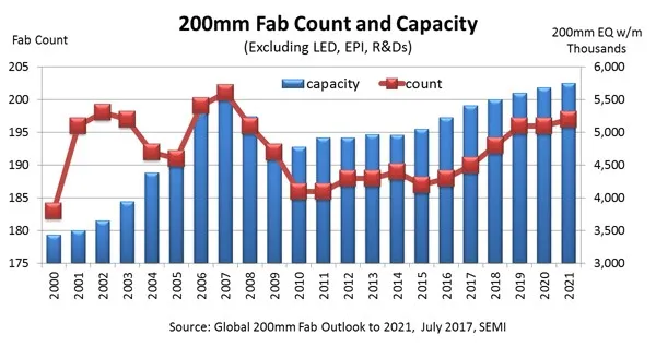
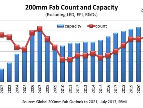
Foreign investment, which fuels technological innovation, productivity, and broad-based growth, is critical to the semiconductor industry’s long-term success. That stream of billions of dollars in investment, however, is at risk of narrowing as a result of the industry’s growing scrutiny by the Committee on Foreign Investment in the United States (CFIUS).Over the last two years, CFIUS, a government body formed to review sales and transfer of ownership of U.S. companies to foreign entities, has denied sales of Aixtron and Lattice Semiconductor to Chinese investors because of national security concerns. More recently, CFIUS rejected the sale of Xcerra to a Chinese company, and the Committee has reportedly become involved in Broadcom’s bid to take over Qualcomm.As highlighted recently, the Foreign Investment Risk Review Modernization Act (FIRRMA) was introduced by Sen. John Cornyn (R-TX) and Rep. Robert Pittenger (R-NC) in November to reform CFIUS, whose form and function have remained unchanged for over a decade. In the spirit of more effective governance that matches global trends, we welcome efforts to ensure that CFIUS better balances global commerce and national security. FIRRMA contains important reforms to drive new efficiencies within CFIUS to help alleviate its rising workload, including devoting badly needed resources to the committee. Among those reforms is the codification of regulations to ensure that a Senate-confirmed appointee with direct responsibility for investment reviews is installed in each CFIUS agency. Notably, however, FIRRMA fails to adequately address several existing problems with CFIUS and, in some cases, creates new ones. First, this legislation dramatically expands CFIUS’s authority, including allowing it to review any non-passive investment by a foreign investor in a U.S. critical technology or critical infrastructure company, even if the investor does not have control over the company. By defining businesses as a critical technology or critical infrastructure company, FIRRMA would subject companies, and not transactions, to review. This means that transactions from a critical technology company that involve non-critical technologies would be subject to unnecessary, time-consuming, and costly CFIUS review. Second, FIRRMA would require the committee to review joint ventures or any other common arrangements that involve sharing intellectual property with a non-U.S. partner. As a result, CFIUS, for the first time ever, would be charged with reviewing outbound international commercial activity. We believe that this is a serious flaw in the bill that would only duplicate the existing U.S. export control regime while adding another layer of regulatory burden. Third, FIRRMA would create different tracks for CFIUS scrutiny based on the origin of the investors. Countries of special concern, like China or Russia, would be subject to enhanced review while other countries with an approved CFIUS-like body, or that have a defense treaty with the United States, would be fully exempt from CFIUS review. This inherent bias seems to challenge the central tenet of U.S. investment policy – non-discrimination. Lastly, FIRRMA establishes provisions for expanded consultation and information sharing with allies. These provisions could lead, even if unintentionally, to needlessly divulging proprietary information and technology. Over the past year, there’s been greater focus on the stronger enforcement on foreign commerce and the protection of U.S. industries. FIRRMA fits squarely in this area. However, instead of creating sweeping barriers with economy-wide implications, a better approach would be to have higher fences around select items. This would help maintain the current investment stream that is vital nourishment for the semiconductor industry and the broader economy while also protecting national security. SEMI will continue working to open new markets while reducing the regulatory burden that can stifle cross-border trade and commerce. In addition, SEMI will continue to educate policymakers on the critical importance of unobstructed trade and investment in advancing semiconductors and the emerging technologies they enable. If you are interested in more information on foreign investment, CFIUS, or FIRRMA, or in how to be involved in SEMI’s public policy program, please contact Jay Chittooran, Manager, Public Policy, at [email protected].
Read More
The White House has released its fiscal year (FY) 2019 budget proposal just as Congress secured a two-year budget deal that will begin the process of wrapping up the rest of FY 2018 and set the government’s top line spending for FY 2019 as well. Included in both of these plans are funding levels for government agencies that are crucial to the basic research underpinning many of the building blocks for future innovation in the semiconductor industry. Funding for the National Science Foundation (NSF) and the National Institutes for Standards and Technology (NIST) are two of the biggest drivers for basic research in the U.S. government, with many other smaller agencies playing a role as well.In a bipartisan compromise, Congressional leaders agreed to a deal that would lift their self-imposed spending caps for FY 2018 and pump an additional $68 billion into non-defense discretionary spending for FY 2019. They now have until March 23 to approve a detailed spending plan for the rest of this fiscal year before moving on to complete the FY 2019 plan by the end of September. While the final spending levels for individual agencies have yet to be finalized for FY 2018, the additional funding bodes well for both NSF and NIST, which had seen cuts of between 2 percent and 9 percent in earlier drafts of spending bills.Meanwhile, the president’s FY 2019 budget plans to flat fund NSF for the next year, while making cuts to NIST of over 30 percent. Included in these cost reductions are proposals to eliminate the popular Hollings Manufacturing Extension Partnership, which provides assistance to small and medium-size manufacturers throughout the U.S. With the program providing funds to states with up to a 50 percent match, its elimination will face strong opposition from both parties in Congress. The president’s budget cuts also target the popular Advanced Research Projects Agency for Energy (ARPA-E) for elimination. Disbanding the agency would end multiple streams of funding for innovations in energy production and storage.While it is the responsibility of the president to submit his budget for the funding of the federal government, the power of the purse resides with Congress. The process of federal funding has been drawn out more than usual this year, with a short-term government shutdown even playing a small role. With the budget agreement now in place, the rest of the funding for FY 2018 should come by the upcoming deadline, with hopes that Congress can then quickly pivot to FY 2019. With the midterm elections coming in November, however, political implications will play an outsized roll in the process for the remainder of the year. SEMI strongly advocates for the position that funding of basic research is closely linked with our nation’s economic prosperity in the modern global economy. Effective research funding as a national priority should be bipartisan and must be backed up by a strong and united community of stakeholders and advocates in the business, research, and education communities. In addition, this funding must not only be robust but consistent and not subjected to the uncertainty of short-term stop gap budget measures. If you’d like to learn more about SEMI’s public policy program, please contact Jamie Girard at [email protected].
Read More
As China embarks on the Made in China 2025 plan with electronics and semiconductor technology as one of the Top 10 focus areas, China's semiconductor industry has an unprecedented growth opportunity. However, besides the huge investment required, the China IC industry is faced with strong competition in terms of technology, products, talent, and supply chain access from many leading global layers in an increasingly interconnected world and a highly global semiconductor market.To be successful, it is critical that China's semiconductor industry speed up its integration into the global industry supply chain. The goal is to achieve sustainable growth through “win-win” collaboration with global partners and leveraging industry platforms to become a significant player and partner in the international semiconductor manufacturing industry ecosystem.China Semiconductor Industry GrowthIn recent years, many new 12-inch fab projects have been announced, started construction, or in ramp-up stage in China, including UMC in Xiamen, PSC in Hefei, TSMC in Nanjing, YMTC in Wuhan and Nanjing, as well as GLOBALFOUNDRIES in Chengdu. Many China-based foundries are adding 12-inch capacity including SMIC fabs in Shanghai, Beijing and Shenzhen, and HLMC in Shanghai area. The production capacity of these ~20 new fabs is expected to come online in the next three to five years.SEMI has seen active interest in several local cities in attracting global and China-based companies to set up semiconductor fabrication facilities. The strong trend for expansion and investment shows no signs of slowdown in China. The current investment fever in semiconductors in China is a balancing act ─ it will lead both to the development of a regional industry supply chain and the demand for capital investment in China. However, as with any expansion bubble, new production capacity in some mature nodes might create overcapacity and raises questions of sustainability paired with the severe shortage of skilled workers/engineers and uncertainty of future fund availability for continuing operations and investment.Rise of ChinaChina’s expansion in semiconductor manufacturing should be viewed through a global context. SEMI advocates for free trade and open markets, international cooperation for intellectual property (IP) rights protection, industry Standards, and environmental protection. SEMI promotes the global electronics manufacturing supply chain and works to positively influence the growth and prosperity of its members.In 2016, before stepping down, the U.S. Obama administration delivered a report from the Council of Advisors on Science and Technology. Part of the report addressed the rise of China's semiconductor industry and recommended the United States should improve its environment for development of the semiconductor and high-tech industry and continue to invest in advanced technologies.Each country will evaluate their own course as the China market expands. However, the rise of the semiconductor industry in China need not be viewed simply as a threat to the world; instead, it is a significant growth driver and business opportunity for global suppliers. IC chips top the list of all Chinese bulk imports in terms of dollar value. China desires to develop its IC chip industry to better fulfill its inherent demand. China currently has low market share and limited technical capability in four major areas identified in the China National IC Development Guideline: IC design, manufacturing, package/testing, and equipment/material.China is clear about its intentions with regard to growing its own semiconductor supply chain. In the short term, heavy dependency on foreign suppliers (especially equipment and material) is inevitable. Going forward, cooperation with foreign semiconductor suppliers/partners with an open-minded and “win-win” attitude is an imperative strategy in solving the development bottleneck issues concerning equipment/materials and other key areas in China's semiconductor industry.Learn more about developments in China by visiting the “Window on China.”
Read More
This is an exciting year to be in the semiconductor industry: semiconductor-related companies are trading at all-time highs and most expect record device shipments and revenues as well as equipment revenues. This growth is primarily fueled by demand drivers such as Automotive Electronics, Medical Electronics, Mobile Phones, and Industrial Electronics. With this recent growth spurt and the proliferation of end-market applications that consume ever increasing numbers of semiconductors, it is tempting to conclude that the industry has seen the end of cycles.At the annual SEMI/Gartner, Bulls Bears Industry Outlook symposium, Stifel’s Patrick Ho, asserted that “Gone are the days of your grandfather's cycles.” Robert Marie of Semiconductor Advisors, maintained that “Cycle shape has changed due to demand drivers, consolidation, maturation and other factors.”However, Gartner’s Bob Johnson was quick to assert, “Whenever people say that cycles are over and that the industry is going to grow forever ─ the industry is at a peak.” He noted that Gartner expects semiconductor revenues to surpass $400 billion this year, increase two percent next year, but decline in 2019. He indicated that Memory is driving this year’s market expansion but will drag down market growth next year as pricing gains achieved will be lost beginning in the fourth quarter of this year. The softness in 2018 is expected to have a detrimental impact on the industry’s spending plans. Gartner predicts that capital spending will shrink to just under one percent next year and contract 7 percent in 2019.In addition to softer memory pricing in the near term, Gartner does not anticipate that China will invest significant amounts until 2020/2021. SEMI on the other hand is currently modeling an increase of 9 percent in fab equipment expenditures in 2018, which is largely driven by China. China is expected to have an even greater impact on global fab capital expenditures, claiming the top position in 2019, according to SEMI.Looking at demand drivers, more specifically the “Internet of Things”, it is clear that the explosion of connected “things” is fundamentally reshaping our industry. The fragmented nature of these markets require niche applications and device architectures with the majority of these devices being commoditized MEMS and other solid-state sensors. Growing market revenue does not necessarily translate into industry profitability as the declining average selling price.So how can the industry benefit from all of this connectivity? Dr. Sam Wang from Gartner discussed how the Internet of Things has made AI practical, and how artificial intelligence brings out the value of IoT. He noted that AI: Drives the demand for advanced wafer process technologies Encourages the adoption of HMC, HBM, eDRAM, ReRAM, PCM, STT-MRAM, memristors processing in memory Incorporates ADC within sensors and computing in sensors Increases the use of 2.5D, 3D, TSV and SiP technologies Enables chip design flow optimization in EDA Fuels the need of new ATE testers for testing complex AI chips Prompts more start-ups and M A opportunities The overwhelming majority of semiconductor devices used in IoT are commodities, creating a renaissance for smaller wafer diameter fabs (200mm and smaller; see related 200mm article). The value of the IoT will come from the ecosystem that supports it, such as data centers and networks that enable connectivity. There are also opportunities for the adoption of new processor technologies, as Gartner’s Werner Goertz pointed out. He stated that the current processors used in IoT processing were designed for very different use cases, and that conditions are now ripe for a disruptive processor supply chain to optimize edge-based AI.2017 is indeed going to be a great year for the semiconductor industry: device average selling prices have improved dramatically, device manufacturers are investing in new capacity, while stock prices of suppliers throughout the supply chain are trading at elevated levels. 2018 is anticipated by many industry pundits to be another growth year, albeit at more conservative growth levels. Although the Internet of Things literally offers the industry billions of applications, its full impact on the industry remains to be seen. And we’ll definitely keep a close eye on developments in China.For SEMI market research, visit www.semi.org/en/MarketInfo
Read More
In the shadow of other more trendy news about China and Memory fab investments, 200mm fabs continue to “flex their muscles.” At least 500,000 wafers per month (wpm) capacity, or a 10 percent expansion, is forecast for 200mm fabs from this year through 2021. This includes capacity from a number of new 200mm fabs expected to start operation in 2017. The recently published report "Global 200mm Fab Outlook to 2021" by SEMI is tracking production, pilot, and R D 200mm facilities worldwide with a special focus on capacity expansions and new facilities. Driven by mobile and wireless applications, IOT, and automotive, the 200mm market is thriving. Many of the products used in these applications are produced on 200mm wafers, so companies are expanding capacity in their facilities to the limit, and there are nine new 200mm facilities in the pipeline. Looking only at IC volume fabs, the report shows 188 fabs in production in 2016 and expanding to 197 fabs by 2021. China will add most of the 200mm capacity through 2021, with 34 percent growth rate from 2017 to 2021, followed by South East Asia with 29 percent and the Americas with 12 percent. SEMI’s recent publication of the “Global 200mm Fab Outlook report to 2021” (July 2017) is the third update since the report was first launched in 2015. Since the last release in November 2016, the SEMI Industry Research and Statistics analyst team has made 232 changes and updates to 132 fabs. The report tracks over 300 facilities using 200mm wafers from R D, EPI, LED fabs to volume IC fabs. For more information, visit: https://discover.semi.org/global-200mm-fab-outlook-registration.html
Read More
SEMI reported that worldwide sales of new semiconductor manufacturing equipment are projected to increase 19.8 percent to total $49.4 billion in 2017, marking the first time that the semiconductor equipment market has exceeded the market high of $47.7 billion set in 2000. In 2018, 7.7 percent growth is expected, resulting in another record-breaking year ─ totaling $53.2 billion for the global semiconductor equipment market. The SEMI Mid-year Forecast predicts wafer processing equipment is anticipated to increase 21.7 percent in 2017 to total $39.8 billion. The other front-end segment, which consists of fab facilities equipment, wafer manufacturing, and mask/reticle equipment, will increase 25.6 percent to total $2.3 billion. The assembly and packaging equipment segment is projected to grow by 12.8 percent to $3.4 billion in 2017 while semiconductor test equipment is forecast to increase by 6.4 percent, to a total of $3.9 billion this year. In 2017, South Korea will be the largest equipment market for the first time. After maintaining the top spot for five years, Taiwan will place second, while China will come in third. All regions tracked will experience growth, with the exception of Rest of World (primarily Southeast Asia). South Korea will lead in growth with 68.7 percent, followed by Europe at 58.6 percent, and North America at 16.3 percent. SEMI forecasts that in 2018, equipment sales in China will climb the most, 61.4 percent, to a total of $11.0 billion, following 5.9 percent growth in 2017. In 2018, South Korea, Taiwan, and China are forecast to remain the top three markets, with South Korea maintaining the top spot to total $13.4 billion. China is forecasted to become the second largest market at $11.0 billion, while equipment sales to Taiwan are expected to reach $10.9 billion. The following results are in terms of market size in billions of U.S. dollars: The Equipment Market Data Subscription (EMDS) from SEMI provides comprehensive market data for the global semiconductor equipment market. A subscription includes three reports: the monthly SEMI Billings Report, which offers an early perspective of the trends in the equipment market; the monthly Worldwide Semiconductor Equipment Market Statistics (SEMS), a detailed report of semiconductor equipment bookings and billings for seven regions and over 22 market segments; and the SEMI Mid-year Forecast, which provides an outlook for the semiconductor equipment market. For more information or to subscribe, please contact SEMI customer service at 1.877.746.7788 (toll free in the U.S.). For more information online, visit: https://discover.semi.org/equipment-market-data-registration.html
Read More
By Clark Tseng, Industry Research Statistics Group, SEMI China’s ambitious plans to build a world-class semiconductor manufacturing supply chain domestically certainly has the industry’s attention. With over a dozen new 300mm fab announcements lately from Foundries, DRAM, 3D NAND, and as well as CMOS image sensor companies (either from international semiconductor makers or from indigenous players), China has launched a huge investment in wafer fab capacity that is expected to ramp in the next five years. While advanced 300mm fab investment attracts most of the attention and resources, China does not skimp on the more “matured” 200mm fabs. China will have the most new 200mm fab projects and capacity additions in the next few years compared to other regions. According to SEMI’s latest 200mm Fab Outlook report, China currently has about 700,000 wafers per month (wpm) installed fab capacity, and this is forecasted to surpass 900,000 wpm by the end of 2021, or over 28 percent growth in five years. By then, China’s 200mm capacity is expected to surpass America, Japan, and Taiwan, and be second only to Europe. A further examination of China’s new 200mm fab projects shows a wide diversity in products. Beyond the usual 200mm foundry investment led by SMIC and Hua Hong Semiconductor, an increasing number of new projects are focusing on analog, power, and MEMS applications. According to SEMI’s latest 200mm fab Outlook report, China will add eight new 200mm volume fabs between 2016-2021: two for foundries, two for analog, two for MEMS, one for power, and one for logic. In the meantime, China is not limiting itself to adding wafer capacity. It is also developing material and equipment capabilities around 200mm wafer manufacturing. A number of silicon wafer suppliers are emerging in China targeting 200mm and smaller wafer markets. On the equipment side, the 200mm tool availability remains the biggest challenge for the industry in adding more 200mm capacity; some projects have been postponed because of it. China equipment suppliers are expected to take the opportunity to develop the tool sets needed to satisfy the upcoming demand for these fabs. China’s 200mm capacity will evolve to make more than “legacy” products, e.g., smart card, Analog IC, and Discrete IC. These manufacturers will become more versatile advancing into MCU, PMIC, CIS, fingerprints sensor, power, MEMS, and other devices. With the rise of China’s electronic OEMs and automakers, these 200mm fabs will play an even more important role supporting various manufacturing ecosystems in China. For more information, visit https://discover.semi.org/global-200mm-fab-outlook-registration.html
Read More