downloadGroupGroupnoun_press release_995423_000000 copyGroupnoun_Feed_96767_000000Group 19noun_pictures_1817522_000000Member company iconResource item iconStore item iconGroup 19Group 19noun_Photo_2085192_000000 Copynoun_presentation_2096081_000000Group 19Group Copy 7noun_webinar_692730_000000Path
Skip to main content
Default Banner Image

Bob Smith

Today’s post is the last of four Q A-style feature posts based on presentations during SEMICON West 2025’s “The Convergence of Semiconductor Manufacturing and Design” organized by the ESD Alliance (ESDA).Bob Smith interviewed Joe Kwan, Director of Product Management from Siemens EDA, about his presentation, “3D Design Brings Multi-physics Requirements While Manufacturing Yield Improvements Require Digital Twin Modeling and Ingesting Design Data.” They covered a range of topics from partner collaboration and integrated design flows to digital twins, AI and more.Smith: How does Siemens EDA define collaboration between design and manufacturing? What does that look like?Kwan: Manufacturers and designers have been cooperating for a long time. The most familiar example is the design rule check (DRC) rule deck provided by the foundry to the design team. It enforces designers to adhere to the layout rules that must be followed for a design to be manufacturable. What’s different now are new problems arising from the latest advances in technologies. Close collaboration is needed between the design team and foundry to identify and share data necessary for a successful final product. Foundries are challenged to encapsulate information that provides design teams with critical information for success without divulging proprietary data.Smith: Can you elaborate with a few examples of what technologies you are referring to that are driving these new collaborations?Kwan: Sure. A great example is the industry’s move from monolithic single chip solutions to chiplet-based solutions that require 2.5D, 3DICs, heterogeneous integration and the like. These approaches require multi-physics simulations to verify physical phenomena in ways that were not necessary when previously focusing on just a single chip design. Thermal, electrical and stress are not independent variables anymore.Design teams need to understand how these effects come in to play with functionality, performance and other design specifications. Most important, they need to be aware of factors that could cause the chip or system to fail. To do this, close collaboration between all parties involved (design team, foundry and packaging) is required so designers know what to look for in their analyses and what to avoid. It adds a whole new layer of complexity necessary for getting to the finish line.Smith: I imagine some scenarios that fit into what you are talking about. For example, if the design includes stacked die, the team will need to be concerned about heat distribution and potential hot spots in the stack. Kwan: That is a good example. Heating problems cannot be overlooked. How does the heat escape from the stack? What is the thermal profile across the stack from the die on the top all the way through to the bottom of the stack. Is there a sufficient pathway for heat to get out? We can do rough estimates early on to see if putting this die on top of this other one, is it going to work? Or be reliable? Back of the envelope calculations might show that the dies need to be positioned differently or even designed differently. Smith: What can be done to improve design success?Kwan: This is where collaboration comes in. The product owner should establish a cross-domain team of experts from chip design, package engineering and process engineering. The product spec and design decision trade-offs must be evaluated against impact to all domains.EDA also plays a critical role. EDA is the link between designers, packaging and manufacturing. We hear and capture concerns from designers and package engineers. We prototype solutions, collaborating with packaging and IC manufacturers to encapsulate requirements for successful production.Smith: At SEMICON West, we also talked about how design data can help foundries during the manufacturing flow.Kwan: Yes, going back to our discussion at SEMICON West, I spoke about that important topic, which is embodying design data into the manufacturing platform in the context of a digital twin for virtual metrology.In an ideal world, we would measure everything. If we could do that, we would have all the data needed to make perfect manufacturing decisions. But it would be extremely expensive. What we can do instead is apply AI virtual metrology. We collect the usual sparse metrology and then combine design data to train a predictive engine. The result is the ability to accurately predict where metrology was not collected.With traditional process-of-record, foundries run a qualification wafer every 10 or so wafers. That’s very expensive. With virtual metrology, we can predict when drift becomes significant enough to blow up a wafer and you can intervene to restore individual nominal tool performance.Smith: Engineers are writing their own agents to automate parts of the design flow such as analyzing the outputs of simulations.Kwan: We see a lot of interest in AI and Agentic AI. There is a lot of potential to improve engineering productivity. But as we race to develop Agentic AI flows, we must also approach this in a rigorous manner that cross-checks to ensure accurate and robust results.About Joe Kwan Joe Kwan is the Product Director for Calibre AI/ML Fab Solutions at Siemens EDA. He has more than 30 years of experience in the EDA semiconductor industry. He previously worked at VLSI Technology Inc, COMPASS Design Automation, Silicon Access Networks and Virtual Silicon. Kwan received a Master of Science degree in Electrical Engineering from Stanford University and a Bachelor of Science degree in Computer Science from the University of California, Berkeley. Robert (Bob) Smith is an independent consultant who has been involved directly in multiple roles in the EDA industry over the past 38 years. His career experience spans analog engineering, marketing, sales, business and strategy development and others including numerous c-suite roles. He holds a Master of Science degree in Electrical Engineering from Stanford University.
Read More
Lu Dai, Vice President of Technical Standards at Qualcomm, presented “Converging Chip Design and Manufacturing in the Era of High Integration” at SEMICON West in October 2025, offering an insightful look at how design and manufacturing are collaborating effectively.I had an opportunity to talk at length with Dai and asked him to define collaboration. His thoughtful answers, perspective on industry trends and what it will take for a seamless automated flow between design and manufacturing made for a great discussion.In addition to his role at Qualcomm, Dai, who lives in San Diego, is Chairman of Accellera Systems Initiative, Chairman of RISC-V International and Director of Silicon Integration Initiative (Si2).Smith: Qualcomm is a fabless company. How do you define what collaboration is between design and manufacturing? Dai: When we talk about design and manufacturing collaboration, we need to consider how a design is optimized for a certain manufacturing process. For example, will an advanced manufacturing capability help designers simplify designs or allow them to bypass traditional actions?I compare it to the way software was optimized to hardware because of hardware limitations. We had to make sure the C code was compact and that the variable types we specified wouldn’t waste memory. We also had to write the code in a certain sequence to speed up the execution of the code. As hardware capability grows, we can write dirty code and it isn’t as critical. We understand the manufacturing process capability. That allows us to be more flexible about where to focus the chip design effort based on needs for power, performance, area, and schedule. We want to make sure we know the chip size and how big the silicon space is for certain features. For example, low power is often a key feature of today's designs. As manufacturing process nodes improve, power goes down and area shrinks. We can therefore focus more on optimizing performance.This is the kind of collaboration we use with foundries. Libraries need to be optimized for the design and tweaked for yield. This collaboration is critical for foundries pushing leading-edge nodes in the design house—they have to work closely with the design team.Smith: And how about collaboration with packaging suppliers? Dai: I'm not a packaging expert. Traditionally, packaging is one of the important steps and even more so because of the push toward the use of chiplets. Packaging becomes really important when dealing with multi-chiplet types of design. Traditionally, IP vendors sell a license to use the register transfer level (RTL) code, which is subject to IP theft. With a chiplet approach, they sell a netlist, which often becomes a hard coded chip as a bundled service instead of a single IP. The subsystem sales approach makes more money, creating another opportunity or a new landscape. SoC companies may get into the IP business and conversely, IP companies are getting into the SoC business by selling the bundled subsystem. Smith: The margins are getting blurred. It sounds like there is collaboration and it’s between designers, but also the foundries, process and the packaging.Dai: And partially between EDA tools because both the design side and the manufacturing side are speaking two different languages. EDA is somewhere in between, helping the translation.Smith: What are the trends and challenges that make it hard or even prevent a fully integrated flow?Dai: The extremely high costs of doing the implementation for an advanced node, especially for the first tape out. If we are the first to use the newest node, we know there is a tremendous benefit in the long run. But we are also the pioneers that have to work out the tough challenges. Few companies have the technical capability and deep financial resources to be the pioneers for a new process node. We’re starting to see high-flying semiconductor companies use leading-edge nodes. On the design side, they are challenged and trying to run faster by adopting a newer node. Cost is probably the biggest challenge for this collaboration. If their margins get challenged or they need to be a little bit more careful, they adapt by becoming fast followers.Another challenge comes from more specialized designs. There has been a long period where general-purpose chips are used for many different applications. But, we are now seeing designers increasingly focus on more specialized chips with custom designs.Custom IP and ASICs are becoming trendy. Designers are trying to figure out how to make a general baseline and then differentiate on certain IP and the best possible manufacturing process for the application. Doing a custom chip on an advanced node is quite expensive. We may be challenged if we don’t have sufficient data to clean up a process because every chip and process combination is unique. Lessons learned from this chip may or may not apply to everyone, while a general-purpose design tends to be a good baseline for lessons learned.Smith: How do you envision an integrated automated flow between design and manufacturing? Dai: In today's environment, we would like an RTL design to be fully portable to any kind of manufacturing process or foundry. Based on our architectural and business, we could then pick and choose the fab and the process. How do we port a design into a new process? That's difficult because we need to consider special constraints required by the new process that didn’t apply to the previous process. There's also the reverse case for porting a new design into an old process.Let’s say we have a chip designed for a 3-nanometer process and we want to port it back to a 28-nanometer process. Why would we want to do this? Imagine a COVID type of situation—a supply chain constraint and/or a geopolitical flare up with no access to the advanced fab, but an older local fab is still available. In this case, we need the chip for the feature it provides. Perhaps a car needs that chip and it was designed to be produced in a three-nanometer process but is suddenly unavailable. A 28-nanometer chip that runs at half of the speed might do the job for a few years. Unfortunately, this is somewhat wishful thinking because of the challenge of the flow. We didn’t think about it but we have to do it now and need to consider whether we have sufficient time to work out the challenges.Smith: How do you make that decision for making chiplets? Dai: Porting to another process is not a small job. It's labor intensive going from a same design in one process to another process.The project lead presents a process porting non-recurring engineering (NRE) cost budget to management. The questions span resources and time needed that boil down to how much money will need to be invested to achieve the porting. It should be simple. It’s not. It’s a lot of work.For many companies, the strategy is to offload the porting to a low-cost geographical team with a cheaper NRE that matches management expectations for the costs of process porting. History often shows that the company is not reducing that much time and manpower by offloading the porting. Smith: What about the EDA tool side? Is there typically a team from the EDA vendor? Dai: For advanced nodes, we involve the EDA and in-house EDA experts when certain parts of our design don't work out as expected.Back-end tools need experts involved in the debugging. And if we don't have an in-house expert, we need our EDA vendors to send engineers to work on the project.Smith: I have a generic question about AI. We talked about reporting. Where would it fit in collaboration?Dai: Sooner or later, we're going to be asked for a proper supply chain tracking or hardware bill of materials (BOM). Conceptually easy, but difficult in practice because it goes from logic design to physical design all the way to manufacturing. How do we carry that type of information through each step with EDA tool providers and manufacturing equipment providers? Their credentials need to be registered and they can’t alter any of the existing flow credentials.Supply chain tracking can ensure that if there's any kind of natural disaster or geopolitical issues, the hardware BOM is properly categorized, and the chip can be made. Security is another reason for supply chain tracking. Collaboration between design and manufacturing is important because once a netlist is sent to the foundry, our job is to make sure it is done correctly. We wait for our silicon to come back. Then we do testing. But during manufacturing, the chip comes back and it doesn't work. How do we know if somebody tampered with it? Supply chain tracking could help.Smith: How can you know that someone didn’t tamper with a chip design after it was handed off to manufacturing? This could cause big issues for end markets such as medical, automotive, defense and aerospace applications.Dai: The solution is EDA heavy because EDA tooling can help on the traceability at every step. It’s all automated through some kind of tool. If we need to have a proper format, we need to have proper encryption. And we know when we use this tool to run it, we check to show we are using the real tool not a hacked version that doesn't have the security credentials.Smith: Will this drive supply chain tracking or drive new standards?Dai: I hope so. Once upon a time, there was an initiative by the Department of Defense to track the supply chain. It was a mandate and no one liked it. It’s much better for the industry to proactively come up with a standard for a global economy.A mandate tends to come from one government. It may be a good mandate if we do business only within one country or within a small region. What if we have to do business with another government that may not like our mandate? Say a certain part of our design stage is done in a different country and we need this level of detail. Who's doing the work and what's the tool version? Per local government rule they may not be willing to give the information to us. This might be sufficient. We don't know the details of the risk, but we know there is a risk. We could simply add to our tracking that a portion of design is done in a foreign country with foreign EDA. It's important to have an industry standard and an international standard so that we can procure our tools and the services around the world instead of being limited.Smith: How can we encourage companies and people to want to cooperate and sign on to a project like this?Dai: With lessons learned, we can go deeper. Maybe the first level is a meeting in the U.S. About Lu DaiLu Dai is Vice President of Technical Standards at Qualcomm Technologies, Inc., spearheading semiconductor standards efforts and relationships with industry organizations. Lu was previously Senior Director of Engineering and led Qualcomm’s SoC design verification team and front-end methodologies and initiatives. He was also the Design Verification Lead responsible for multiple generations of premium tier platforms at Qualcomm, including the Snapdragon 8 series and products that power the Mars Perseverance rover and Ingenuity helicopter. Prior to Qualcomm, Lu was the Design Verification Lead for Cisco’s Gigabit Switching Business Unit where he worked on multiple generations of Cat4k ASICs. Lu is the current Chair of Accellera, Chairman of the RISC-V International Board of Directors and serves on the Board of Directors at Si2. Lu holds a Master of Science degree in Electrical Engineering from Cornell, and a Bachelor of Science in Electrical Engineering and Computer Science from UC Berkeley.Robert (Bob) Smith is an independent consultant who has been involved directly in multiple roles in the EDA industry over the past 38 years. His career experience spans analog engineering, marketing, sales, business and strategy development and others including numerous c-suite roles. He holds a Master of Science degree in Electrical Engineering from Stanford University.
Read More
Aki Fujimura has been at the forefront of chip design innovations from the beginning of his career and his technology leadership continues today. He serves as Chairman and CEO of D2S, co-founder of the eBeam Initiative, President of BACUS, and a Governing Council member of the ESD Alliance, a SEMI Technology Community. At Tangent (now Cadence), Fujimura and Steve Teig (a chip designer for the last 20 years and now Vice President and Distinguished Engineer at Amazon) built the first commercial over-the-cell routing system dedicated to fully synchronous designs with timing assurance and automated test-scan insertion. Fujimura and Tom Kronmiller developed LEF/DEF for efficient representation of Manhattan routing, both used as standards in the automated place and route (P R) flow to this day. He again teamed with Teig and Kronmiller to develop the X Architecture, an interconnect architecture based on the pervasive use of 45o diagonal routing. I was thinking about his background as I called him to chat about his evolution from chip design before focusing on chip manufacturing via eBeam technology at D2S.Smith: Let’s talk about your journey from focusing on how to do physical design of chips to chip manufacturing. How did this happen?Fujimura: GPUs weren’t a thing until late 1990s. With CPUs, Manhattan design was the obvious choice for computational efficiency. Largely gridded metal n that went up and down, and metal n+1 that went left and right with vias to connect the line segments were how all automated layout worked. PCB routing and packaging (even back then) used diagonal routing and even curved routing. But chip P R was all Manhattan. That was still true when we worked on the X Architecture at Simplex Solutions (now Cadence). ATi (now inside AMD), NVIDIA and several other GPU companies started in the late 1980s to 1990s, but they were targeting video and gaming more than scientific computing at the time. It’s when Teig came up with the idea for the X Architecture that he wanted to know if 60-degree routing was possible “because a hexagon tessellates a plane.” A good question. I set out to try to find out what the actual limits were in manufacturing that create the limitation to Manhattan shapes. I got introduced to the late Bill Arnold of ASML, who then introduced me to a lot of people in manufacturing who helped me get the answer. Naoya Hayashi of DNP was instrumental in helping me understand that mask making is where the limit exists. Hayashi-san kindly explained to me about the two mask writers. I had to dig around a lot more to make sure that that was the only barrier, but that’s how I came to understand that before masks, everything is data, and after masks, everything is physical. Mask making is the key that enables 45 degrees, but not 60 degrees. The lessons I learned then are still very important to me today. That’s when I saw and appreciated the opportunity there is for software for semiconductor manufacturing.Smith: But you still couldn’t use GPUs for the X Architecture work?Fujimura: Right. Way too early. The idea that GPU-accelerated gaming machines can be connected together to do video editing, or that large scientific simulations can be done on a connected set of gaming machines, was being explored in the 1990s already. It was only 20 years ago (2006) when Jensen Huang announced his bet with the CUDA software stack for general purpose GPUs (GP GPUs) for nodes in racks of CPUs, GPUs, memory and communication to create the modern scientific computer. Six years later in 2012, AlexNet won the ImageNet Large Scale Visual Recognition Challenge (ILSVRC) with CUDA, and the rest is history. But no, we didn’t use GPUs at Simplex. But we did help design GPUs, including with the X Architecture.Editor’s Note: ILSVRC evaluates algorithms for object detection and image classification at large scale. Smith: Now, everything you do at D2S is with GPU acceleration. When and how did that change come about?Fujimura: It was back in 2009, two years after D2S was founded. An extraordinary engineer, Harold Zable, noticed that simulation-based manipulation (rather than rules-based manipulation) of mask shapes, both for wafer manufacturing and for mask manufacturing, would be the ideal application for GPU acceleration. Fast-Fourier Transforms (needed for lithography simulation and optical proximity correction (OPC)/inverse lithography technology (ILT)) and Gaussian manipulations (needed for eBeam mask simulation and mask process correction (MPC) are nearly “free” in terms of compute time on GPUs. You still have to get the data in and out efficiently, but you can do pretty sophisticated computing without much overhead. At the same time, multi-beam based eBeam writing was getting momentum, first in wafer direct write applications. In 2007, at the BACUS conference in Monterey, Calif., IMS—then a well-respected research organization in Vienna—published a paper saying that multi-beam for mask writing is what they’d like to do. The wafer market is much bigger, but this technology is more suited for mask writing, where write times are measured in hours per mask. “Wafers Per Hour” is the measure in wafer manufacturing, so mask writing gets to flip the division. We were looking at a mask design and mask manufacturing world that should be doing simulation-based manipulation rather than rule-based. That’s better with GPUs. On top of that, maybe the world is going to go to multi-beam writing, going away from four decades of variable-shaped beam (VSB) writing. And I knew from the X Architecture experience that VSB was the only thing in the eco-structure that restricted mask shapes to be Manhattan or 45 degrees. In fact, with multi-beam, any curvilinear shape within the limits of resolution of a given pixel size can be freely written on the mask. The only barrier then to having curvilinear masks would be the software stack and trying to compute it with CPUs only. We knew GPU acceleration was the answer. Smith: Was it just totally an accident that multi-beam and GP GPUs happened at the same time?Fujimura: Yeah, it was. However, just as when multiple people simultaneously invent the same thing without knowing about each other, the environment and times in which we live have a lot to do with this. So, I guess, it’s not really just “luck.” But GP GPUs in 2006 and IMS Multibeam in 2007, I think that’s luck.Anyway, D2S became the GPU-acceleration partner for the semiconductor manufacturing industry and decided to work only on things that can be accelerated by GPUs in 2012.Smith: What trends do you see going forward in the next three to five years?Fujimura: A move toward curvilinear mask features, as well as an increased interest in curvilinear wafer targets as designers become aware that the manufacturing side has established a solid path for curvilinear mask shapes. We’re leaving a lot of margin on the table to accommodate gridded Manhattan assumptions, and that’s really no longer necessary from a manufacturing standpoint. I think electronic design automation (EDA) should be working on enabling curvilinear designs, because the door is open for the design world to explore curvilinear chip design and to reap compelling benefits in terms of power/performance and reliability.Editor’s Note: While Manhattan geometries are rectilinear shapes aligned to vertical and horizontal axes, curvilinear design introduces smooth, continuous curves into layouts and masks, leveraging advanced computational lithography and mask-writing technologies. This improves pattern fidelity, electrical performance and manufacturability at advanced technology nodes.About Aki FujimuraAki Fujimura is chairman and CEO of D2S, Inc., and managing company sponsor of the eBeam Initiative. Previously, Fujimura was CTO at Cadence Design Systems, President/COO and inside board member of Simplex Solutions, and VP and inside board member at Pure Software. He co-founded Tangent Systems (acquired by Cadence).Fujimura, made a SPIE fellow in 2023, serves as President of the SPIE BACUS Technical Group. He serves on the governing council of the ESD Alliance, a SEMI Technology Community. Fujimura was on the board of HLDS, RTime, Bristol, S7, and Coverity, Inc.Fujimura received his BSEE and MSEE degrees from MIT.Robert (Bob) Smith is executive director of the ESD Alliance, a SEMI Technology Community. 
Read More
Presentations from SEMICON West’s “The Convergence of Semiconductor Manufacturing and Design” offer great insights into the collaboration between the two, as I was recently reminded by presenter Sutirtha Kabir, R D Engineering, Executive Director at Synopsys.Reviewing his talk “Revolutionizing Silicon to Systems Design: Unlocking the Future with 2.5D and 3D Multi-Die Innovations” was a good kick-off for our discussion that covered the continuous need for collaboration and where AI fits. Kabir, as I quickly learned, is a technical innovator and articulate communicator passionate about ongoing collaborations between design and manufacturing. Today’s blog post is the second in a four-part series featuring presentations from the SEMICON West design program, organized by the ESD Alliance, a SEMI Technology Community. The first blog, with Dave Kelf, CEO of Breker Verification Systems, appeared on January 6 (“Circular Collaboration Leverages EDA Advances”).Smith: How do you define collaboration between design and manufacturing?Kabir: Multi-die design and advanced packaging are a big focus of high-performance computing (HPC) and AI chips. Engineers are trailblazing and foundries are coming up with new stacking combinations. For this reason, design and manufacturing teams need to be closer than ever. Solutions must be made available to give ample visibility to manufacturing from the very start of the design process. Single die design has been done for 15 to 20 years with a continuity of power, area, and performance (PPA). Design flows, methodologies and the ecosystem between design houses, EDA vendors and foundries are mature and stable. The conundrum is that it's a different situation with multi-die designs. Not only is multi-die emerging rapidly, but the types of design innovations are different.We have been working closely with our foundry partners to move multi-die innovation forward by enabling more advanced process and packaging technologies. I don't see this slowing down as they are coming up with different ways of doing designs. Design teams are collaborating closely with the foundries to take advantage of the benefits of these new multi-die designs.Smith: You mentioned new stacking combinations and collaboration with the foundries. What about collaboration with the OSATs? Kabir: Generally, it’s both silicon foundries and OSATs. With advanced packaging, both play a significant role depending on the types of applications being targeted. Design house targets may shift from the traditional silicon foundry to several OSATs. For example, if an organic interposer is required, the collaboration could be with an OSAT in conjunction with the silicon foundry. There are many possible collaborations that may be required. The point I’m trying to make is that there is a strong need for collaboration between EDA and the foundries during design that continues through manufacturing and test.Smith: What trends in general are driving the need for this collaboration?Kabir: The trends are performance and scalability and the need for high-performance compute. Look at some of the mega-chip systems coming out today compared to the bigger systems from five years ago. HPC was not driving that much in 2.5D. The big interposers used to be on silicon, maybe 1.2 to somewhere around less than three reticle sizes. Today, the reticle limit is more than 5X. Leapfrog to today, and the configuration has changed where the state of the art is to use an organic interposer with multiple embedded bridges (up to 20 or more) buried inside the interposer to support high-speed interconnect. The organic interposer with multiple layers on the front side and back side communicates with bridges and the SoC and HBM that sit on top of that interposer.3D architectures stack dies with GPUs and a large amount of HBM such as an HBM4 memory stack. The memory stacks may be 8 or 16 high. All of this memory needs to be as close as possible to compute for scalability. In terms of the high-power demand, the designer needs to make sure that the voltage that is pushed from the bottom of the stack can feed the power hungry SoC blocks on top of the 3D stack. At the end of the day, EDA is all about giving design and manufacturing houses the capability to predict how a design is going to perform in all different kinds of scenarios. EDA must keep up with this trend and that requires collaboration.Smith: What about the verification side, specifically system verification? Kabir: Let’s say I am using a spreadsheet and doing back-of-the-napkin calculations, a technique that used to work well for single die or design blocks. Multi-die doesn't scale since multiple heterogeneous dies in a single package must be considered. Design planning must include directional changes to measure the effects with key performance indicators. The challenge is to correlate signoff and verification. Signoff engineers can no longer just verify at the end of the design cycle. Instead, it has become a continuous process that transcends the flow from design planning through implementation and signoff and release to manufacturing.The industry is repeating a pattern from about 20 years ago, when single-die design evolved from relatively naive approaches to much more sophisticated EDA-flow-driven methodologies.Smith: As you drive the tools forward, who are your counterparts on the manufacturing side? Kabir: It depends on the different stages of design—design planning, implementation or signoff. It starts at the architecture stage from the left when architects and physical design engineers are doing floorplanning. The term design technological co-optimization (DTCO) has evolved into S (system)TCO now because we are trying to co-optimize system design and technology. I'll give you a simple example. A working chip manufactured in a certain technology node is going to be used in a multi-die design. Is the existing chip technology good enough to support the design or will it require a new chip at a different node? In either case, how does an engineer work with the manufacturing house to make sure it has the right metal layers or a different number of metal layers or a different metal width or some other property on the technology side? Designers need to make data-driven decisions based on the configuration and technology numbers to meet power budgets.In the past, what was once managed through designer-ASIC house-manufacturing interactions are now increasingly being handled by EDA flows as part of design implementation.Smith: Ultimately, it's driven by business. The hard work and decisions are made by two teams of knowledgeable technical people who must come together.Kabir: And then of course it has to be rolled into program management, business development and all this needs to be supported by data. We all recognize that the design window is not increasing. It’s always about trying to get more out in less time with less people. That doesn't help the equation.Bob Smith: How does AI fit into this and how is it best leveraged? Kabir: I’m hearing, learning, and reading about the tremendous advantages AI could bring. AI has a huge role to play, but it won’t eliminate the need for savvy design and verification engineers.Multi-die design brings together different users from different tool backgrounds. Even the language between a packaging person and a silicon person is different. The terminologies they use are different, as are the ways they have done design over the last 15-20 years. The same applies to thermal, power or signal integrity engineering. Bringing them together requires that EDA will provide platforms where the whole system design, including chip design, is managed. That’s a tall ask for people from all different backgrounds to come in, learn different technologies and tools within a short time. This is where ChatGPT or Microsoft’s Co-Pilot can be applied in the EDA world today to quickly find solutions by reading through manuals, application notes, forums and the like to find solutions. This use of AI agents can save tremendous amounts of time for designers. Another aspect that can be positively impacted are roles. We have customers coming to us and brainstorming on the use of workflows and methodologies, instead of the design aspect. Scalability from the human perspective has become difficult because of the need to closely guide engineers to get them up to speed on new technologies and workflows. This is where Agentic AI can deliver a huge productivity boost. It's not replacing anyone. It's getting them to decisions and end results faster.Smith: Can Agentic AI play a big role? Kabir: Current AI is like the person who, when asked a question, has to give an answer even if it’s the wrong answer. The same thing is going to happen when we bring in all these EDA technologies with AI capabilities.The point I'm trying to make is how do we verify that AI is doing the right thing? In EDA, one of the biggest questions and concerns is if a result or outcome or design can be verified. If it can't be verified accurately, verification engineers will not trust what AI is telling them no matter how fantastic the algorithm is. The verifiability of AI solutions is important for EDA. The key question is: Why would I trust what your tool is telling me to do?EDA flows that are more mature rely on decades of expertise, thorough documentation, and various scenarios to train AI algorithms. Those are the AI-powered EDA flows that I trust the most. About Sutirtha KabirSutirtha Kabir, an Executive Director of R D for Synopsys’ 3DIC Compiler, has over 20 years of product engineering experience, driving, building, and inspiring teams across companies in the EDA industry. In his role at Synopsys, he supports construction and analysis of multi-die systems including stacked ICs plus Interposer configurations. Prior to joining Synopsys, Kabir was a Group Director of Engineering at Cadence. Kabir has a Master of Science degree in Electrical Engineering. Robert (Bob) Smith is executive director of the ESD Alliance, a SEMI Technology Community.
Read More
The SEMICON West 2025 design program “The Convergence of Semiconductor Manufacturing and Design,” organized by the ESD Alliance (ESDA), a SEMI Technology Community, featured presentations about successful collaborations between the design and manufacturing markets. The three-hour program in a packed conference room included plenty of great material that we’re using as the basis for a blog series that you will see over the next several months. I’m working on them now based on my conversations with four of the speakers where we discuss key drivers behind the need for collaboration and what’s ahead.I’m starting with Dave Kelf, CEO of Breker Verification Systems, a company steeped in front-end chip verification, who describes an actual circular collaboration that effectively leverages AI and other electronic design automation (EDA) advances. We recently talked about collaboration, integrated design and manufacturing flows and AI.Smith: How does Breker define collaboration between design and manufacturing? Kelf: In general, at a technical level, we would define this collaboration as the sharing of data, methodology and/or information that improves both processes. As semiconductors become more complex, this sharing process is increasingly important to effectively manage the overall complexity of today’s chip designs.Smith: What trends are driving the need for this collaboration?Kelf: Apart from the ever-increasing size and density of semiconductors, there are specific trends that require more interaction between design, verification and manufacturing. Obvious developments include the advent of chiplets, given the changes in performance of signal paths, and 3D devices driving complex packaging, power dissipation and other issues. Design issues such as the increased need for SoC coherency testing and complex device structures such as multi-core processors, also play a role. With many of these issues, design and verification (D/V) trade-offs have an impact on manufacturing, and vice versa. For example, differing delays on a Universal Chiplet Interconnect Express (UCIe) interface—an open specification for a die-to-die interconnect and serial bus between chiplets—will have an impact on hazard testing in coherency verification. As another example, thermal hotspots on some parts of a chip package might need additional testing during the verification phase. Smith: What trends and challenges are preventing a fully integrated design and manufacturing design flow?Kelf: Traditionally, the D/V and manufacturing teams have remained separate in most organizations, as well as between the two industries. EDA companies sell primarily to the design teams, although they do interact with the foundries at the back end of the process. Manufacturing companies work directly with different teams at the foundries and not with the D/V teams at all. New relationships need to be built up. The general know-how in these disciplines is different, and methodology approaches tend to be disconnected. The tradition is to separate the processes and use standardized interfaces for communication that leaves little room for improvisation. All this needs to change so that teams can begin to work more closely.Smith: What is circular EDA-manufacturing collaboration and vertical integration?Kelf: In past EDA flows, we have seen disparate tools performing specific functions. As semiconductors got smaller, their physics changed and this led to the design process absorbing new characteristics. For example, abstract designs were run through synthesis to create gates connected by wires. This format was then passed to place and route (P R) tools that would lay out the gates in terms of transistors and interconnects on the silicon wafer. On large devices, the gate level signal delays were larger than the interconnect, allowing design to be separated from layout. As silicon became denser, the interconnect delays became the dominant factor, and the layout of the device impacted the design synthesis process. The two tools required forward integration—synthesis projected layout rules to P R, and a reverse integration where layout characteristics were sent back to synthesis for redesign where required delays could not be handled during P R. The methodology went from a simple flow to a circular design approach as synthesis and P R cooperated. The same is now true of design and manufacturing where solving the problems noted above requires this same circular cooperation. Smith: What will it take to have an integrated design and manufacturing flow?Kelf: A lot of cooperation between different groups. As we reach limits in areas such as signal integrity and thermal management that will squeeze silicon efficiency improvements, these methodology linkages will be required for continued progress and growth. The industry (both design and manufacturing) will be highly motivated to make this happen. Smith: From a personnel perspective, who (on both sides) are the typical touchpoints? Kelf: It will be the engineering staff from both the design side and manufacturing that work closely to develop technical solutions. Executive-level support is, of course, needed to cement the collaboration. Smith: Where does AI fit?Kelf: AI will have a role to play in this. Estimating the factors that drive efficient design to manufacturing to design flows is a critical step in speeding interaction and providing sensible estimated starting points. AI can process the large amounts of data necessary to provide these estimates as we now see complex chips that contain billions of transistors. AI will be needed to accelerate the interactions for different tools through the development process.As design and manufacturing collaboration becomes a critically important industry strategy, companies are turning to SEMI and its Technical Communities such as the ESDA and their wide-ranging initiatives. For details and to get involved, visit the ESDA website at https://www.semi.org/en/communities/esda. To learn more about Breker and its solutions that provide test content portability and reuse to solve complex semiconductor challenges across the functional verification process, go to: https://brekersystems.com.About Dave KelfDave Kelf holds the position of CEO of Breker Verification after serving as its Chief Marketing Officer responsible for all aspects of Breker’s marketing activities, strategic programs and channel management.Earlier, he served as vice president of worldwide marketing solutions at formal verification provider OneSpin Solutions, was president and CEO of Sigmatix, Inc., and held senior positions at Cadence, Synopsys and Springsoft. Kelf holds a Bachelor of Science degree in Electronic Computer Systems from the University of Salford and a Master of Science degree in Microelectronics from Brunel University, both in the U.K., and an MBA from Boston University.Robert (Bob) Smith is executive director of the ESD Alliance, a SEMI Technology Community. 
Read More
Maheen Hamid is a co-founder of Breker Verification Systems, supplier of functional verification solutions for complex chip design challenges, and serves as its COO and CFO. She is also Co-Chair of the ESD Alliance and member of the SEMI North America Advisory Board (NAAB).Given her background, roles within the industry and interests, it seemed like a good time for me to reach out for her perspective and market analysis. During our discussion, she offered up some great observations, identified trends, pointed to areas in need of attention and ways for the industry to better collaborate. We ended by talking about AI’s role today.Smith: How do you track where the semiconductor industry is going?Hamid: Business and macro strategies have always been interesting to me. In recent years, with the increasing global importance of silicon sovereignty, it is necessary to track the pulse of initiatives across various channels in multiple geographies. Starting with policy discussions at SEMI to media coverage of the semiconductor value chain to EDA specific news, I read voraciously and listen in on disparate discussions. There is no denying that it is impossible to envision the boundaries of where the semiconductor industry could go, particularly in design innovation. Smith: Nonetheless, what trends have you identified?Hamid: Global trade wars are creating as many roadblocks as they are creating opportunities. It is fascinating to watch the incredible innovation led by the U.S. for decades in semiconductor design be challenged as technology and access to technology gets democratized across the board. Maintaining thought leadership is a demanding task and no longer contained to an individual company’s cleverness. Crafting an effort that is coordinated with national interests has become compulsory. Separately, developments in AI are creating a new wave of complex chip designs that are redefining hardware investments. Data centers are becoming as ubiquitous as the personal computers of the ‘80s. While advanced chip designs forge ahead and additional classes of chips such as memory become truly commoditized, the need for efficiency in the full flow from design to manufacturing becomes imperative to protect margins for relevant players.Smith: The need for industry collaboration appears to be a trend that is an essential part of the industry’s evolution. How do you see that developing in chip verification?Hamid: RISC-V has given rise to many new design starts by companies that do not have the legacy verification frameworks owned by the NVIDIAs and Intels of the world. Several of these larger customer companies are investing heavily in their own complex chip designs, creating interesting opportunities for a collaborative approach to enabling internal innovations. As well, this new class of customers is less married to enterprise flows from large EDA companies and prefer to invest in best-of-breed solutions. This is driving necessary collaborations across EDA vendors in chip verification. Driven by mutual customer demand, we have recently modified several of our arrangements with other EDA players.Interestingly, the momentum in the RISC-V ecosystem is also driving new initiatives in the more traditional flows. This is a necessary shake-up in how business needs to be done in an increasingly, globally competitive landscape. Smith: What area do you see that needs more attention?Hamid: It is imperative to keep the business climate conducive for innovation and thought leadership. Policy debates impacting the chip industry are getting more heated and controversial. We need more concerted collaboration among the players in the chip ecosystem to help influence this policy in a way that allows U.S. companies to thrive. We need to promote more opportunities that bring disparate companies together to build clever flows that increase our silicon sovereignty. Smith: AI is playing in the design and design tools area. What about other parts of an organization, such as finance or operations and marketing?Hamid: AI efficiencies can help with predictive analysis for large companies in these core functions such as finance, operations and marketing, but for smaller, nimble companies, the human element still rules. Our strategic marketing, as an example, is defining industry-leading initiatives. AI does not have access to language models to automate any of what we need to invent in communicating new ideas. LLMs do provide a good sounding board though. It’s interesting to “discuss” ideas with ChatGPT and pull templates of successful implementations in unrelated industries that could be a blueprint for how we approach next steps.About Maheen HamidMaheen Hamid is the co-founder CFO and COO at Breker Verification Systems, bringing a wealth of financial engineering experience from investment banking and small business management. Hamid has been instrumental in establishing Breker as an important stakeholder in the EDA industry, running its business side and driving operational growth as it thrives as an established software supplier. She plays an active role in defining the company’s strategic direction, corporate communications and branding. Hamid holds a BBA from North South University and an MBA from the University of Texas at Austin.Robert (Bob) Smith is executive director of the ESD Alliance, a SEMI Technology Community. 
Read More
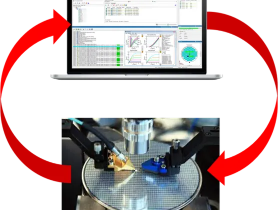
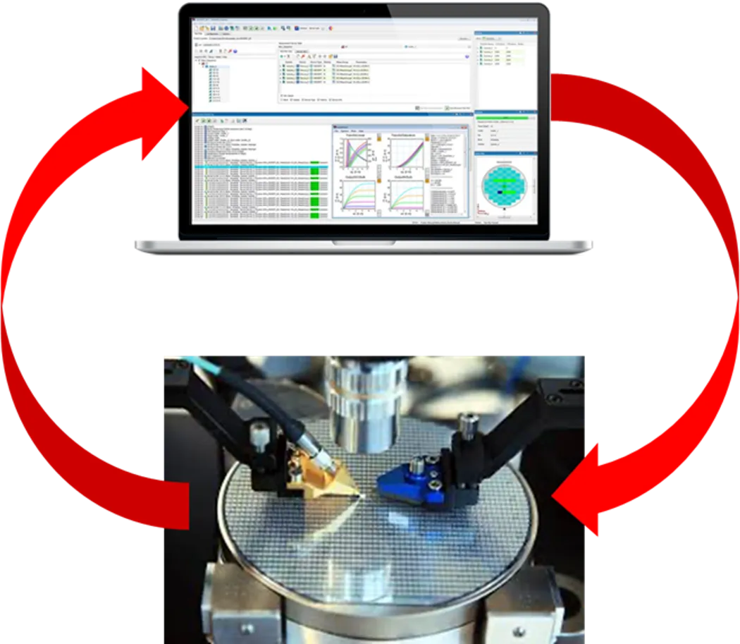
John Kibarian, CEO and co-founder of PDF Solutions and a member of the ESD Alliance (ESDA) Governing Council, will deliver a keynote during the CEO Summit at SEMICON West in October titled, “Revolutionizing Semiconductor Collaboration: The Emergence of AI-Driven Industry Platforms.” He recently shared with me a summary of what his talk will cover and his perspective on why collaboration is the key to growing the semiconductor industry to $1 trillion and how we will get there.Smith: What is the major industry evolution or dynamic that's making collaboration essential today?Kibarian: The semiconductor industry has dramatically evolved from a simple, linear process to a complex, collaborative ecosystem. Previously, everything happened at the wafer fab. Testing occurred at wafer sort, package yields were high, final testing was straightforward, and products were shipped. Collaboration was mainly between foundries and fabless customers, intensive during early qualification and test chip stages, then evolved to routine yield monitoring once production stabilized.Today's advanced packaging puts multiple chiplets into single packages, creating an explosion of test insertion points. This has driven up both test complexity and costs significantly. Front-end fabs now house the most complex machines, while test and assembly facilities, once relatively simple, now feature sophisticated system-level testers with integrated robotics. Assembly tools have become highly complex, with die-attach processes requiring increasingly tight tolerances. Success now requires collaboration across the entire chain, from system companies to equipment vendors, both for new product launches and ongoing production maintenance.Companies are adopting AI and machine learning (ML) to manage these complex production flows, whether for testing or equipment control. This demands even broader collaboration since AI requires combining data from multiple sources across foundries, fabless companies, OSATs, equipment vendors, and more, data that no single entity controls. What was once a straightforward handoff between two parties has become an intricate web of interdependent relationships requiring continuous coordination.Smith: Chiplets and chiplet-based architecture is in the news and seems to be a key solution or practical solution in response to the slowing down of Moore's Law. This demands incredible levels of collaboration and coordination across the whole value chain. Is this doable at scale where it starts to move into the mainstream?Kibarian: The semiconductor industry will need unprecedented collaboration to make chiplet manufacturing work at scale. But this can be done! Consider EUV lithography: Initially expected during the 65nm generation, it took years longer than anticipated despite being an incredibly complex technology. Extraordinary engineering was needed but it also required extensive collaboration between ASML, suppliers, customers, and the broader fabless community.If the industry achieved this level of coordination for EUV, it can do the same for chiplets. However, chiplet manufacturing will require even greater collaboration as more companies will build systems using chiplets from multiple suppliers.Today's chiplet-based systems typically source all components from one manufacturer, making standards like UCIe less critical since companies control their entire supply chain. This will change as companies increasingly use third-party components for cost-effectiveness.More and more, we will see systems using components from multiple players to get to market more cost-effectively. Consequently, future production flows will be significantly more complex, requiring coordination of substrates and base dies, third-party dies and interposers, OSAT and specialized testers with specific configurations.This orchestration must work not just for initial bring-up but for the ongoing production as well, and when reconfiguring chiplet combinations for different products, all requiring rapid, automated responses.All of that must be automated for quick reaction. Considering the complexity of the manufacturing flow, people will want to apply AI/ML to anticipate what is going on in each individual product built.Manual oversight of every chip and package during manufacturing isn't feasible at scale. Automated AI agents must handle this monitoring and quality control. Expanding this automation will require close collaboration between the manufacturing entity and engineering teams at the product companies.This will also require a different level of alignment and orchestration across all the software packages managing this complex multi-company process. The financial enterprise resource planning (ERP) systems know where material is going, what the demand is, and what the forecasts are. While separately, the manufacturing execution systems needs to know which tools are going to be available when. Most often, these manufacturing systems operate in factories the product company doesn't own. The product company’s PLM systems control the bill of materials and test flows, but these tests will be conducted at the OSAT requiring complex coordination between the software systems of multiple companies controlling different process domains. This orchestration spans organizational boundaries and must be able to take data from upstream test results and make decisions on what tests to run downstream. This is required to get the right chiplets put together into a package in an efficient manner within a short cycle time and not require a Formula 1 pit team to keep everything running.Smith: The volume of data is staggering, especially now with design data. What will it take to enable this vision, at scale, where everything's connected? Kibarian: It’s a marriage of the human establishing the bounding box within which the systems operate that employ agents to do a lot of the work on a day-to-day or hour-by-hour basis. A good example is how manufacturing execution systems (MES) connect to ERP systems to share data. When a company sets up an orchestration, it creates rules that govern how information flows between systems. These rules tell the ERP system: "To calculate costs for each process step, here's the recipe information you should use."Once these rules are in place, they work like guidelines that control daily operations. An AI agent automatically creates insights based on actual data collected from the MES and moves data between systems according to these rules. The ERP AI agent will use this data to spot when costs are rising and send alerts, to notice when production yields drop, to calculate what lower yields mean for costs, and will take action to fix problems.This same process happens between equipment suppliers and manufacturing facilities. They share data automatically based on pre-set rules, and AI helps identify issues and take corrective action. Fabs determine who can access which machines and when, what types of data can be transmitted and through which channels, and how frequently these transmissions occur. When new software or AI models are introduced to run equipment, the systems specify what virus scanning and security checks must be completed before installation.Human operators primarily configure these control systems by determining the most effective collaboration protocols. However, the day-to-day execution is handled by automated agents due to the enormous scale involved, both in terms of data volume and the sheer number of transactions that occur continuously throughout operations.A human will not go through and review that data. I'll give two examples of this. One outside of our industry and one in our industry. At our 2019 user conference, board member Marco Iansiti, a Harvard Business School professor, shared insights from his book on AI in business. He compared traditional banks with Ant Bank, Alibaba's banking arm, which was experiencing explosive growth before Chinese government intervention.Ant's AI wasn't particularly sophisticated, but its process was revolutionary. While traditional banks require customers to fill out loan applications that then go to human loan officers for review, Ant's system would automatically scrape the internet and social media to verify applicant information. Within seconds, an algorithm would approve or deny the loan.The crucial difference is that Ant could scale exponentially because its only constraint was computing power. Traditional banks need to hire more loan officers to double their business, a human bottleneck that limits growth.I invited him to speak because I believed in this principle six years ago, and I'm even more convinced now.For the semiconductor industry, to build a trillion-dollar industry with complex, integrated systems, we need to minimize human intervention in data intensive processes. Despite the trust issues between stakeholders in our sector, collaboration remains essential. The solution requires establishing systematic principles that allow AI agents to operate autonomously. This is a way forward to achieving exponential growth.The Ant Bank example perfectly illustrates what our industry needs. At PDF, we believe this approach is crucial for industry advancement. Consider this: We manage petabytes of data, yet humans only examine 5-10% of it. This shows AI's potential to handle the vast majority of operations without human oversight.The reality is that our customers build millions of chips a week, billions a year. They cannot look at every dataset. Algorithms can, AI can. We launched a product called Guided Analytics last year. An engineer spoke about it during our user group last year. Her company has a couple of thousand products. Her group could not keep track of them every day, but Guided Analytics could. When her group came in the morning, the daily report noted 90% of the chips were fine or alerts pointed to where issues are. It's a simple AI bot crawling over data and identifying where the root cause seems to be.Our industry will require more agents to scale. Those agents will span the industry, and yet we as humans need to set up the governing principles under which they can operate. That's how we're going to deal with the massive amounts of design and manufacturing data to get the velocity the industry will need, and to benefit from the AI that we create for our businesses.Notes: Kibarian’s keynote, “Revolutionizing Semiconductor Collaboration: The Emergence of AI-Driven Industry Platforms” is scheduled for Wednesday, October 8, at 10:20 a.m.SEMICON West adds design to its program with “The Convergence of Semiconductor Manufacturing and Design” to highlight the collaboration between semiconductor manufacturers and chip design teams to bring advanced systems to market. The three-hour session will be held Tuesday, October 7, from 1 p.m. until 4 p.m. Learn more about the design program in our latest blog. SEMICON West 2025 will be held in Phoenix, Arizona from October 7-at the Phoenix Convention Center. SEMICON West’s homepage has links to the full program, including more details about “The Convergence of Semiconductor Manufacturing and Design,” special features, sponsor and exhibits. Registration is open. About John KibarianJohn K. Kibarian is President, Chief Executive Officer and Co-Founder of PDF Solutions. He has served as President since 1991 and CEO since 2000. Dr. Kibarian received a Bachelor of Science degree in Electrical Engineering, a Master of Science and PhD degrees in Engineering Computer Science from Carnegie Mellon University.Robert (Bob) Smith is executive director of the ESD Alliance, a SEMI Technology Community. 
Read More
Electronic Design Automation (EDA) financial analyst Jay Vleeschhouwer, Managing Director of Software Research at Griffin Securities, carefully tracks the design portion of the semiconductor industry and offers insightful analysis used by this community. He also presents the State of EDA, a yearly report on EDA, during the Design Automation Conference (DAC). After this year’s presentation, he and I talked about trends, the difference between EDA and Architecture, Engineering, and Construction (AEC), security and chiplets. A condensed version of our talk follows. Smith: Now that the Synopsys-Ansys merger closed, what changes? Vleeschhouwer: Synopsys is now the largest company by revenue and backlog in all of Engineering Software, a well over $30-billion industry, including all the parts of that market—AEC, EDA and Technical Software. The pro-forma backlog, about $9.84 billion as of the most recently reported quarter, is the largest in the industry. An important question is how will Synopsys integrate, employ and leverage the four-fifths of Ansys that is not strictly EDA? That is, other than Ansoft and Apache, the two entities that mostly comprise Ansys' EDA, and that ties into the convergence theme. Also, the question in any acquisition is the balance between leaving the operations and the portfolios as they were, or not. In other words, let them continue doing what they were doing if they were doing it well or quickly absorbing, integrating and leveraging those portfolios into the buyer's portfolio. That roadmap is something that we would be interested in hearing more about in terms of its purely EDA aspects and as well the convergence aspects.Smith: Have you observed any new trends in 2025 that surprised you? Vleeschhouwer: The short answer is that it's more of the same in terms of the main technical and business trends. Of course, the most recent important exogenous effect is the advent of tariffs and new export restrictions, or the variability around export restrictions. That's perhaps the main thing that's occurred in the last few weeks and months. We're seeing a continuation of trends that have been in place for a number of years in terms of many of the technical and business results that we've highlighted in our reports. From industry data, there continues to be multiple EDA categories that are continuing to grow. It’s observable and important that we see this breadth of product adoption and growth across multiple categories. This has been beneficial to each of the four largest EDA companies. There have been compelling technical reasons for this, and I would expect it to remain the case. In terms of those significant multi-year trends, the answer would be no. Otherwise, in terms of 2025 specifically, the thing that was interesting about this year’s DAC was the presence of more startups, something that we've not seen in EDA for a long time. It's interesting that we are seeing startup activity not only in EDA, but even in one of the other areas of Engineering Software that we cover: AEC has little to do with semiconductors and electronic systems and it too has more startup activity than we've seen for about a quarter of a century. Although the rationales for the startups in these two different areas of Engineering Software are quite different. The rationale for the EDA startups is one set of rationales, whereas in the case of AEC, it's different, which to me is analytically interesting. Smith: What is the difference between the rationales for startup activity in EDA and AEC? Vleeschhouwer: AEC has to do with the design and construction of commercial buildings, residential buildings, infrastructure, meaning roads, bridges, airports, tunnels, civil engineering, public works. Among the companies that we follow in those markets are Autodesk and Bentley Systems. Autodesk has a small connection to EDA because one of their mechanical CAD products has some integration with some PCB design tools. In any case, the rationale for startups in AEC that we've seen has mostly to do with what has been some vocal dissatisfaction with the incumbent or large incumbent products. That's different from EDA, where we can’t make a case that there is dissatisfaction or sufficient dissatisfaction with the incumbent tools that would necessitate, or be a catalyst, for startups. What we're seeing here is the ongoing, complex, rapid evolution of semiconductor design and electronic systems design because of the unusual breadth of EDA tools and functions, far more so than in AEC. There's much more opportunity for niche products to perhaps complement existing tools. As you know, it can be difficult to dislodge an existing tool in EDA. The industry has become consolidated among the big four—Ansys, Cadence, Siemens EDA and Synopsys—and now three with Synopsys/Ansys merger. Backlogs have continued to grow and book-to-bill has been positive for 15 years. It’s hard to infer any dissatisfaction with incumbent tools or insufficient satisfaction showing up in the numbers. Whereas in AEC, it's different in terms of the profile of the customers or the way the tools are used. There are far more customers than in EDA—thousands upon thousands of architectural firms and construction firms and so forth. The installed base of the AEC software is an order of magnitude more than in EDA. It just so happens that there was one tool from Autodesk that has been getting considerable attention from customers in terms of how modern it is and so forth. This created an opening for some startups. Notwithstanding the nominal dissatisfaction with this tool, however, that particular brand continues to grow. It has the largest base in the industry. At the end of the day, the largest product of its kind in the market continues to grow at a decent rate. The vendor in this case, Autodesk, has acknowledged some of the things needed to do to improve the tool, and it's investing toward that. In any case, there are differences in why these startups exist, how they're approaching the market.Smith: The big topics now are 2D and 3D and chiplets. Where is the market relative to chiplet-based design? Vleeschhouwer: It’s still early, based on commentary from the EDA vendors, about developing and delivering the tools. I don't have a precise measure as to how much of the business is attributable to it. It’s still something that has a considerable runway, which is a good thing. As more tools that can enable it come together, then we'll continue to see this cycle of enablement and delivery. That phenomenon will continue to grow. We would love to hear the vendors’ provide more precise attribution in terms of how much of the business is coming from this. For investors, it will be incumbent upon the vendors to be more explicit about the contribution from the new technical phenomena because it is a new growth catalyst. Smith: The ESD Alliance is starting to see more interest in securing the design flow. This is a huge issue. The design flow is more complex and it's going to require cooperation, collaboration and new standards. Vleeschhouwer: Yes. Siemens EDA is the largest in classical product lifecycle management (PLM) or managing the whole process, an important issue for the industrial and manufacturing markets with its Teamcenter product. Interestingly, Siemens EDA still has work to do to integrate Teamcenter with Calibre, which would seem to have been a natural thing to have done, and I think still is. Teamcenter and Calibre are the two billion-dollar brands that Siemens Industry Software has as an entity. Calibre is by far the predominant product of its kind for semiconductor manufacturing. It's got at least two-thirds market share. Teamcenter is the market leader in classical PLM. The connection between those two brands, owned by the same company, would be an interesting executable to observe.About Jay Vleeschhouwer  Jay Vleeschhouwer, Managing Director of Software Research at Griffin Securities, has more than 40 years of research analyst experience in the technology sector, including software, semiconductors and computer hardware. Vleeschhouwer does a yearly presentation on the State of EDA during the Design Automation Conference (DAC). The slides can be found at: DAC presentation (June 2025) 2.pdf Note: The ESD Alliance will host a three-hour design track “The Convergence of Semiconductor Manufacturing and Design” Tuesday, October 7, from 1 p.m. until 4 p.m. during SEMICON West in Phoenix, Ariz. Robert (Bob) Smith is executive director of the ESD Alliance, a SEMI Technology Community. 
Read More
This year’s SEMICON West has new dates, a new location in a new city and a new addition to the program—design! “The Convergence of Semiconductor Manufacturing and Design” will highlight the collaboration between semiconductor manufacturers and chip design teams to bring advanced systems to market. The three-hour session during SEMICON West will be held Tuesday, October 7, from 1-4 p.m. at the Phoenix Convention Center in Phoenix, Arizona.Five 20-minute presentations will describe successful collaborations and address challenges and opportunities about design and manufacturing security, long-term reliability, system performance issues, and modeling and verification that encompass the entire system. Attendees can expect to learn about the key drivers behind the need for collaboration that range from heterogeneous integration to advanced packaging technologies and applications such as automotive and medical.Session moderators are Ming Zhang, PhD, Vice President of Fabless Solutions of PDF Solutions, and me. “As design and manufacturing complexity continues to grow, driven by applications like AI, it is becoming increasingly difficult to account for every manufacturing variation during design and at sign-off or to fully anticipate the entire design space at chip and system levels during manufacturing technology development,” said Zhang. “Achieving tighter integration between design and manufacturing through broader and deeper data and methodology collaboration will be critical to improving predictability, accelerating time to market and enabling the next generation of semiconductor innovation.”It’s within this context that we selected the presenters who include:“Revolutionizing Silicon to Systems Design: Unlocking the Future with 2.5D and 3D Multi-Die Innovations” by Sutirtha Kabir of Synopsys.“Manufacturing to Development to Manufacturing for Circular Collaboration Leveraging AI and Other EDA Advances” with David Kelf from Breker Verification Systems.“Bridging the Silicon Divide: Converging Chip Design and Manufacturing in the Era of High Integration” from Lu Dai at Qualcomm Technologies.“3D and Chiplets Driving Moore’s Law into the Future” with Joe Kwan of Siemens EDA.“Multiphysics Multiscale Challenges and Solutions for 3D Heterogenous Integration” by Sudarshan Mallu from Ansys, part of Synopsys.The program concludes with a panel moderated by Zhang titled “The Convergence of Semiconductor Manufacturing and Design” and features the session presenters.Join us to learn how the semiconductor manufacturing and design communities are collaborating to deliver advanced systems based on chiplets and rapidly emerging packaging technologies including 2.5D and 3D ICs and MCMs. Audience participation will be encouraged.Also of interest to attendees is a SEMICON West keynote from John Kibarian, CEO, President and Co-Founder of PDF Solutions who is also co-chair of SEMI’s ESD Alliance Governing Council. Kibarian will address “Revolutionizing Semiconductor Collaboration: The Emergence of AI-Driven Industry Platforms” during the CEO Summit keynotes on Wednesday, October 8 at 10:20 a.m.SEMICON West 2025 makes its debut in Phoenix, October 7-9 at the Phoenix Convention Center. This milestone event gathers global leaders across the microelectronics supply chain to explore transformative technologies, develop the future workforce and drive strategic collaboration. Moving SEMICON West to Phoenix highlights Arizona as a key hub for innovation and industry growth. Visit the SEMICON West homepage for more details on full program, including “The Convergence of Semiconductor Manufacturing and Design” session, special features, sponsors and exhibits. Registration is open. Robert (Bob) Smith is executive director of the ESD Alliance, a SEMI Technology Community. 
Read More
Ann Wu is CEO of EDA startup Silimate, developer of a co-pilot (chat-based GenAI) for chip and IP designers to find and fix functional and power, performance and area (PPA) issues in their designs. Rick Carlson is Vice President of Sales at ESD Alliance member company Verific Design Automation, provider of front-end EDA platforms to a range of small and emerging EDA companies like Silimate and larger EDA vendors.I recently talked with Ann and Rick who represent EDA’s new and old guard. I found them to be bullish about the emerging EDA space called AI EDA that uses GenAI and large language models as the foundational tools and the swelling numbers of well-funded startups entering this space.Smith: Ann, you were an Apple hardware designer. What encouraged you to leap into entrepreneurship using AI as the foundational technology?Wu: It was always my goal. Apple afforded me the opportunity to understand how one of the best companies producing some of the most cutting-edge chips in the world operates. It also gave me the opportunity to work with some of the most brilliant engineers and operators. My plan was then to go back to Stanford to explore and start a compelling venture with another similarly motivated friend, Akash Levy. That was the genesis of Silimate. The drive for leaping into entrepreneurship then ultimately stemmed from my frustrations with the existing chip design process. I sensed there was an opportunity to apply AI technology to solve some of these limitations of the existing approaches to chip design.Smith: What made you think that AI would be applicable to the EDA challenges that designers face?Wu: AI provides a compelling solution to some of the intractable problems that have existed in EDA. Traditional EDA solutions solve isolated problems through heuristic algorithms. There’s a high volume of gray area between the well-defined boxes of inputs and outputs that had previously been unsolvable. Now with AI, there is finally a way to sift through and glean patterns, insights, and actions from these gray areas.That’s the macro reason why there's so much excitement and appetite around the application of AI for EDA.Smith: It sounds like productivity enhancement. What are some other key words or selling points to use to convince a designer of AI’s potential for EDA?Wu: I would say "speedup" is one of those keywords. Ultimately, the designer is trying to meet or even shorten the time to tape out while hitting their design spec. That's driving all decisions, whether to throw more headcount at closing a certain block or to defeature something that's going to cause the team to miss the shuttle. It all comes down to whether a fully featured and functional design gets to tape out and gets to market ahead of competitors.Productivity as a keyword is not compelling. It’s hard to translate how saving minutes or hours of an engineer's time connects back to the bottom line. The bottom-line decisions are driven by the project’s timeline as time to market is everything.What’s needed is a way to sift out and resolve real design problems 100x faster, which ultimately results in real speed up on a project’s schedule. For example, processing large amounts of data with AI to find issues actively helps the designer converge their design to their target.Finding and resolving issues in a design within minutes instead of days or weeks instead of months is the kind of impact that directors, VPs, and managers want for adopting new tools.Smith: What is driving hardware designers into this EDA space?Carlson: The thing that's most intriguing is large language models, neural networks and AI. It seems like an “aha” moment when startup founders believe they can do something that's dramatic for the first time.When I look back over my photobook of moments in my time in the EDA industry, there's the wonderment. The things that can be brought to bear with iterative versions of new technology from companies like Ann's will offer multiple “aha” moments. This is game changing.Smith: Are venture capitalists investing in EDA again?Carlson: Yes. Some venture capitalists haven't invested in EDA for decades. These are smart people. They have plenty of good people that can do good due diligence. The amount of money that's being invested is significant. It's not just a little bit of seed funding. One startup’s first round was $3 million. They're now raising $20 million in the next round. They're saying that their pre-money has to be $50-$60 million. They're just coming out and there's a huge amount of interest.We're going to be looking back in a year and say we just couldn't believe how much money is pouring into this. It has a huge impact on the world stage. This is an amazing time to be doing anything in and around the design of computer chips.Smith: Y Combinator (YC) invested in Silimate.Wu: Yes, that's right. It's an honor to be the first EDA company that YC had invested in. The semiconductor and EDA space had been under the radar until recently—it’s such a critical piece of our technical infrastructure. The semiconductor industry hasn't been headline news in past years. Now every other day, the Wall Street Journal runs some semiconductor chip-related article. People are realizing this is a fundamental piece of our world's tech stack, and the software that drives this tech stack is equally important and there are investments to be made.Learn more about Verific and Silimate during the 62nd Design Automation Conference (DAC).Verific will exhibit in Booth #1316 at the Moscone Center in San Francisco from June 23-25.Silimate’s Akash Levy, Founder and CTO, will participate in a panel titled “AI-Enabled EDA for Chip Design” at 10:30am on Tuesday, June 24, 2025.Robert (Bob) Smith is executive director of the ESD Alliance, a SEMI Technology Community.
Read More