downloadGroupGroupnoun_press release_995423_000000 copyGroupnoun_Feed_96767_000000Group 19noun_pictures_1817522_000000Member company iconResource item iconStore item iconGroup 19Group 19noun_Photo_2085192_000000 Copynoun_presentation_2096081_000000Group 19Group Copy 7noun_webinar_692730_000000Path
Skip to main content
Default Banner Image

Bob Smith

Machine learning (ML) and artificial intelligence (AI) have ushered in tremendous opportunities for faster growth, problem-solving and technological development in the electronic system design ecosystem. Cadence Design Systems, Inc., a member of the ESD Alliance, a SEMI Technology Community, is at the technological forefront in incorporating ML techniques in its chip design products. I spoke with Chin-Chi Teng, Senior Vice President and General Manager of Cadence’s Digital Signoff Group, about how ML is reshaping EDA and the semiconductor industry, the cloud’s role in the evolution of ML in design and its impact on Moore’s Law. Teng also offers advice on how engineering students can calibrate their education to prepare to work with this transformative technology and urges them to have fun in the process. Smith: How is ML changing the EDA industry? Teng: ML is changing EDA for the better in many ways. It’s more difficult than ever to design chips, and ML is helping by overcoming the complexity, size and technology interdependencies. At the same time, ML is helping our own engineers solve certain classes of EDA algorithm, tool, and flow/solution challenges so that we can deliver even better EDA tools to our user base. The benefits can include reducing runtime, increasing quality of results, and being better equipped to manage vast complexity and data. Also, and maybe even more significant, is the potential boost to user and team productivity, where engineers have more time to focus on high-value problems because they no longer need to spend time on managing overwhelming volumes of data and details that can be easily automated. Smith: What is the potential impact ML can have on semiconductor design? Teng: ML technology can be leveraged in several ways to improve EDA tool performance and engineering team productivity. For example, we initially applied ML to applications such as formal verification, simulation regressions, analog circuit design, and PCB design. We targeted ML toward specific algorithms that processed lots of data to sharpen and speed decision-making. Then we started to look at digital implementation flows that combine multiple steps with multiple decisions in a recipe, especially for chip implementation where the more efficient use of engineering knowledge can make a substantial difference in the chip’s resulting power, performance and area (PPA). These flows present more challenges and require different ML and optimization techniques since the data points are expensive to create and the volume of data is huge. But flow optimization offers the largest rewards for companies investing in data collection and analysis to improve their operations and product quality. By using ML to improve the implementation flow, our users are seeing up to 20% better PPA and 10x improved productivity in developing data center CPUs and AI engines, automotive sensor processing SoCs, and mobile devices. Smith: What is the cloud’s role in the evolution of ML in EDA? Teng: More ML usage means there will be an inevitable surge in compute demand resources, and engineers need the ability to scale in parallel. The cloud provides engineers with the best opportunity to scale computing resources without facing procurement limitations. The cloud also allows engineers to use task-specific compute and ML accelerators and capitalize on distributed computing innovations that leverage the cloud for greater design flexibility and availability. Smith: You have written that you see Moore’s Law accelerating. How does ML fit into this? Teng: We see the rapid adoption of new process technologies as the biggest trend surrounding Moore’s Law right now. ML technology in EDA will help speed tool certification processes, process design kit (PDK) development and other deliverables aimed at creating and improving customer support through all stages of the process lifecycle. This is a virtuous circle, and it’s expanding beyond hardware design and optimization to also include software. Today’s ML functionality works on the abstraction of register transfer level (RTL), optimizing the implementation and verification flows. ML will soon enable use of a higher abstraction of describing the target systems, exploring architectural options and optimizing across hardware and software partitioning. Smith: What advice would you give engineering students who are studying ML with the goal of becoming an electrical engineer? Teng: With the rapid pace of technology development, things are changing constantly. I’d absolutely encourage students to look at ML because ML isn’t going away — its growth is only going to accelerate from here. I’d also suggest that students look more broadly at computational mathematics because that’s foundational for ML. There are many, many opportunities to apply ML to real-world applications that will make a significant impact when it comes to optimizing computational software. Most important, students should explore and have fun while doing it. About Chin-Chi Teng Chin-Chi Teng has served as Senior Vice President and General Manager of the Digital and Signoff Group (DSG) since 2018. Prior to this role, Teng held senior leadership positions in research and development in digital implementation. Teng joined Cadence in 2002 via the acquisition of Silicon Perspective Corporation and subsequently led various research and development groups. He brought deep technical knowledge and more than 20 years of industry and academic experience to his role as leader of the IC Digital group. Teng holds a BS in electrical engineering from the National Taiwan University and an MS and Ph.D. in electrical and computer engineering from the University of Illinois at Urbana-Champaign. He holds seven patents and has written many EDA papers, several deep learning papers, and the book Electrothermal Analysis of VLSI Systems. Robert (Bob) Smith is executive director of the ESD Alliance, a SEMI Technology Community.
Read More
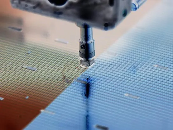
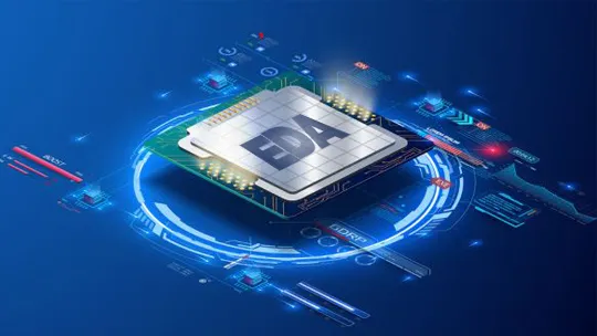
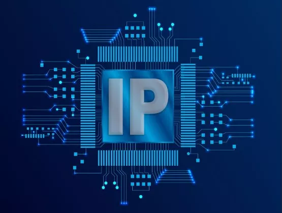
In the early 1990s, engineers of varying degrees of skill with a powerful PC set up shop designing and selling blocks or libraries of reusable components with a defined interface and behavior. These blocks, known as intellectual property, or IP, were then (and still are) integrated into a larger design. While the new market segment created excitement and new opportunities, it also was untested and created uncertainty. Many fledgling companies failed. It’s a different story today. Arm, as well as Cadence and Synopsys, are silicon IP suppliers and the segment’s yearly revenue tops $4 billion, a long way from those early garage startup days. ESD Alliance member CAST, a silicon IP provider since 1993, participated in the remarkable growth and impact on the semiconductor industry. Nikos Zervas, CAST’s CEO, and I discuss those early days of the IP business and what’s ahead. Smith: What were the early days of silicon IP like? Zervas: In those early Wild West days of IP, vendors and customers both wanted to benefit from IP, but nothing was standardized, and people just tried things to see if they worked. The perceived barrier to entry was low: hundreds of IP companies sprang up thinking they only needed RTL coding skills and tools, an FPGA to prototype, and a few thousand dollars to invest. IP deliverables, quality standards, and business practices varied from vendor to vendor and over time. Risk was high, and there are many horror stories of re-spins or market failures due to faulty IP cores. Smith: How has the silicon IP market changed from its early days? Zervas: Firms delivering high-quality IP and providing outstanding customer support survived. Others disappeared. Eventually the industry centered around a reasonably common sense of IP requirements and quality and a consistent set of business practices. 
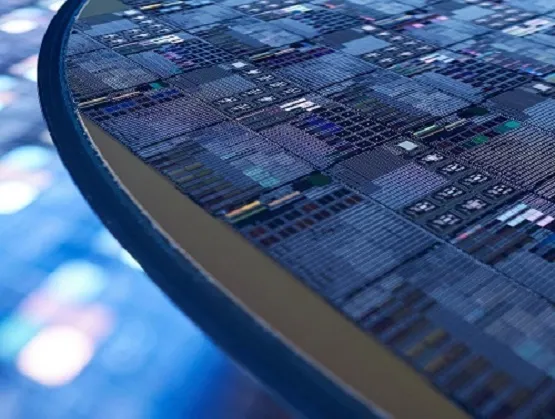
IP product complexity has driven upwards as SoCs have grown. The largest ASICs used to approach a few million gates; today they’re hundreds of millions, and the granularity of IP has evolved from small functions to pre-integrated subsystems. Early on, a designer doing image processing might license individual functions like a Finite Impulse Response (FIR) filter or a Discrete Cosine Transfer (DCT) block. Today, instead they would license a complete JPEG compression core containing those functions and more, or even a complete black box subsystem streaming processed, stabilized, compressed video over Ethernet. IP selection criteria have also changed. Early IP was handcrafted to eliminate every extra gate, as being a few thousand gates smaller was a killer advantage in the era of 180nm ASIC processes. Today, at 7nm or 5nm process, tens of thousands gate differences are just noise, and it’s usually the reliability, functionality, and performance of an IP core that matter most. Smith: When did the silicon IP market start to take off? What was the driving force? Zervas: By the early to mid 2000s, uncertainty about what IP was and how best to use it – and the early wave of less-than-great providers – were being replaced by increasing acceptance and emerging best practices. The introduction of smartphones, the wild growth of Internet of Things applications, growing automotive system sophistication, and other advances fueled the explosion of the IP market in the late 2000s. In fact, according to the ESD Alliance Electronic Design Market Data Report, revenue from IP licensing today has surpassed the license revenue from front-end EDA tools. This would have been unimaginable in the late 1990s. Smith: How has silicon IP changed chip design? Zervas: Designers today must develop massive, complex systems with an even tighter time to market. Only the higher level of design abstraction and the distributed expertise that silicon IP provides make this possible. But IP also increases the challenge of differentiation: With the same IP available to everyone, how do you design a product that stands out in its market? The answer to differentiation today lies mainly in clever SoC architecture. Delivering better features with superior performance, lower power consumption, or other winning characteristics now depends not so much on perfecting each separate IP block but rather from selecting the best IP for the system’s requirements, integrating those IP cores for clean communication and efficient resource sharing, and other smart system-level decisions. It’s similar to modern building design: Every firm has access to the same materials and tools – concrete, glass, etc. – but only a few produce exceptional buildings. Smith: It seems that are several different business models for IP licensing, such as up-front license fees, subscriptions, royalties, or a combination of these. Do you think the IP market will gradually align around one basic model, or will it continue as is with a variety? Zervas: Different models serve different needs. For example, commodity IP like a SPI interface can’t demand royalties, but unique, leading-edge IP – like a 112Gbps SERDES – still can. I believe the market will continue with different business models, though the number of different models may shrink and their terms begin to align. About Nikos Zervas Dr. Nikos Zervas is the chief executive officer of CAST, Inc. He co-founded image and video compression IP developer Alma Technologies in 2001, and led the bootstrapped firm as chairman and CEO for nine years before joining CAST. He was a founding member of the Hellenic Semiconductor Industry Association and served on its board for several years with responsibility for strategic planning. He is a senior IEEE member and member of the Technical Chambers of Greece, had contributed to the GSIA's IP Working Group, and has published multiple technical papers on data compression design and related topics. Robert (Bob) Smith is executive director of the ESD Alliance, a SEMI Technology Community.
Read More
Alameda, Calif.-based Verific Design Automation, a member of the ESD Alliance, made its name in the electronic system design and semiconductor industry supporting companies ranging from startups to billion-dollar industry leaders such as Synopsys, Cadence, Siemens EDA, Xilinx, Microchip, NVidia, Infineon, Qualcomm, Renesas and Samsung. Its software is used as the front end to design automation tools such as synthesis, simulation, debug, and formal verification. I spoke with Verific president and COO Michiel Ligthart about homegrown and open-source EDA tools and other recent trends in chip design. Smith: What trends are you seeing in chip design? Ligthart: Semiconductor companies are starting to build a portfolio of intellectual property, including homegrown electronic design automation (EDA) tools, that they want to keep secure and differentiated from their competitors. The increased interest in internally developed and supported EDA tools is a trend we started to see about two years ago. It’s not simulation, synthesis or place and route (P R). Instead, it’s pieces of a chip design flow optimized for a company’s specific needs. In the past, a semiconductor company would either standardize on one EDA company’s chip design flow or mix and match best-in-class tools from different vendors. The common denominator was that they used off-the-shelf products. If they had a specific requirement, they went to the EDA provider for assistance. In today’s competitive landscape, semiconductor companies are figuring out ways to diversify themselves and their design flow became a way to do so. They may not build their own P R tool, but they will look at building their own power domain approach, for example. Is this a widespread trend? It could be. We hear about it within end-user applications ranging from 5G and AI to data center processors and there are probably others we don’t hear about. Power optimization is an example of the kind of specific internal need being addressed. Smith: What are your thoughts about open-source EDA tools? Ligthart: Our industry supports open source already with language reference manuals (LRMs) for VHDL, SystemVerilog, Unified Power Format (UPF) and the RISC-V Instruction Set. The LRMs and the instruction set are free. Moving to the development of actual tools becomes a question of who will implement, support and maintain the tools. Implementation is expensive. The Big Three (Cadence, Siemens EDA and Synopsys) invest about 35 to 40% of top-line revenue into R D. For smaller EDA companies, this number is even higher. The industry may come up with a business model that will have open-source components as well as a way to fairly reimburse companies that make these tools freely available. I have not seen it yet. Smith: Business Insider reports that Verilog HDL is among the top 10 tech skills that companies are desperate for their employees to learn right. Does Verific get asked about Verilog training? Ligthart: No. Our customers are experienced users. Nonetheless, it was great to read that article and it suggests the semiconductor industry is healthy, growing and hiring talented engineers. Smith: If an entrepreneur asked you for advice about starting an EDA or IP company, what advice would you provide? Ligthart: I would tell the entrepreneur to focus on the problem the startup is solving. Stick to the company’s core competency and try not to build in-house what can be purchased from a reputable supplier. In the end, it will save time and jump-start the development effort, and the engineering budget can be allocated to the startup’s core competency. The external supplier presumably has years of product validation, which brings a major QA gain. About Michiel Ligthart Michiel Ligthart, president and COO of Verific Design Automation, has an extensive background in engineering, product marketing and general management. Prior to joining Verific, Ligthart was vice president and general manager of West Coast operations for Theseus Logic, a startup in asynchronous logic. Before that, he spent eight years with Exemplar Logic in engineering and marketing roles. Ligthart started his career with Philips Research Labs in California and was a visiting scholar at the Center for Integrated Systems at Stanford University. He has a Master of Science degree in Electrical Engineering from Delft University of Technology, the Netherlands. Robert (Bob) Smith is executive director of the ESD Alliance, a SEMI Technology Community.
Read More