downloadGroupGroupnoun_press release_995423_000000 copyGroupnoun_Feed_96767_000000Group 19noun_pictures_1817522_000000Member company iconResource item iconStore item iconGroup 19Group 19noun_Photo_2085192_000000 Copynoun_presentation_2096081_000000Group 19Group Copy 7noun_webinar_692730_000000Path
Skip to main content
Default Banner Image

semiconductors

Innovations in the public sector are springboards for new products in digital health and personalized medicine. Since 2013, SEMI NBMC, funded by the Air Force Research Laboratory (AFRL), has been evaluating industry needs and soliciting proposals for new research into the foundations of device development and manufacturing of medically actionable devices.SEMI NBMC has run 17 separate programs with more than two dozen organizational participants developing materials, electronics, microfluidics, manufacturing processes and algorithms to create low-cost, wearable sensors. Most of these integrated sensing systems communicate wirelessly and incorporate high-performance silicon devices that are designed to move with the individual. Each of the projects was the result of a proposal received during NBMC’s annual proposal cycle. ​What’s Next in MedTech Device Development?We invite you to join the teams at SEMI, NBMC and AFRL to answer that question in a virtual series of sessions over the four weeks in August.For the past five years, NBMC has been conducting similar sessions for roadmapping the development of non-invasive human performance monitoring technology and manufacturing. The information feeds into the topics for upcoming RFPs, including the one we expect to release in September 2020. Previous Workshops (formerly entitled Blood Sweat and Tears) brought together industry and university innovators to explore current product research and provided excellent insights for the proposal evaluation teams. We believe the insights are also very useful to the business and technology planning direction for researchers and developers working on these products.Our focus is on early-adopting markets – medical professionals and their patients, Army and Air Force personnel and high-performance athletes.​ In this time of social-distancing and overall hesitancy to approach hospitals and medical offices, medical monitoring that provides medically-actionable intelligence is of even greater significance.But Doesn’t FitBitTM Have that Covered?Advancements are coming fast and furious – but medical professionals and insurance companies are struggling to distinguish innovations that provide actionable intelligence from those that provide generalized, non-actionable data.The workshop will focus on the medically relevant information that requires a great deal more accuracy, testing and certification before decisions are made. It is the innovations in this field that will lay the groundwork for new products in digital health and personalized medicine. Additionally, they are leading to advancements in aeromedical monitoring and diagnostics to support the U.S. Air Force’s mission to improve patient care during emergency air transport. The targeted future state is real-time monitoring of biochemical and physiological markers that can guide optimization of human performance and health. ​The SMART MedTech Virtual Workshop Series will link markets with manufacturing for medical relevancy – addressing both ends of the ecosystem. This forum will bring together the players across the growing range of industries that are entering or advancing human monitoring applications to:​ share competitive ideas that may be applied to product development​, assess roadblocks in bringing human monitoring products to market, and form partnerships that have become key in overcoming obstacles to successful manufacturing and product development. ​ Join the experts who are at the cutting edge of product design and manufacturing techniques. Indeed, the success of previous workshops was based on the unique membership of NBMC, where product and manufacturing-oriented engineers from industry, universities, and government labs form teams and pool resources (financial as well as technical) to accelerate human monitoring product development into manufacturing prototypes.Can’t Attend the Workshop?All sessions will be recorded and available for watching and re-watching on-demand. Join our interest list to receive regular updates on SEMI NBMC activities, including notification of the RFP expected to be available in October 2020.Find out more about the Smart MedTech Initiative and the NBMC Programs at our website.Rene Krantz is Director of R D Programs Business Development at SEMI. She is the primary manager of SEMI Smart MedTech Initiative and NBMC programs. Contact Rene at [email protected].
Read More
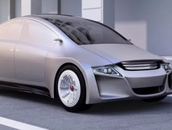
As the amount of electronics in automobiles continues to increase, it is becoming more common to hear a vehicle referred to as a “computer on wheels.” To that end, innovation occurs at the intersection of automotive and microelectronics so that leveraging synergies and contemplating joint initiatives becomes crucial in shaping the future of both fields. In this two-part article, we will discuss the current trends in the automotive industry, which are to a large extent driven by microelectronics, and will reflect on the transition from “just the vehicle” to “the mobility ecosystem.”SEMI encourages its members to partner in seizing opportunities in safe, efficient, and convenient mobility solutions. Before diving into specific opportunities that the automotive industry offers to electronics companies, we will start by taking a closer look at this sector and the current trends.Automotive or Mobility? Shaping the New EcosystemThe automotive industry and its supply chain of vehicle manufacturers and component suppliers has been evolving for decades around the sales of vehicles. The customer groups used to be fairly well established with individual consumers and commercial entities, the latter often as fleets. The automotive industry has grown in depth by vertically integrating design, manufacturing, sales, service, accessories, etc. More recently, the traditional players have also begun to venture into mobility services such as car sharing, showing their ambitions to become “mobility providers.”The term “mobility” has been used increasingly instead of “automotive” for about a decade now. This reflects the more recent transition to creating businesses and functionalities around the sales of miles. In line with this, the industry’s perspective is also shifting toward use-cases and experience rather than just focusing on the vehicle or plain transportation. Much of this transition from “vehicles to miles” is driven by key trends that require massive use of microelectronics, in particular autonomous driving and electric vehicles.One of the key questions to raise for SEMI members is: at which stages should the supply chains for the microelectronics and mobility industries interact with one another to shape the evolving ecosystem? In order to answer this question, we will examine the four main trends shaping the future of mobility represented in the acronym “ACES”: Autonomous, Connected, Electric, Shared.ACES – Autonomous, Connected, Electric, SharedThese four trends, together with the broader transition from “vehicle to miles,” also include newcomers “disrupting” the industry and changing it for good. Basically, every mobility player, traditional or new, is taking ACES (or CASE) into consideration at the moment.Autonomy: computers are taking over the task of driving from humans, first through advanced driver assistance systems (ADAS) and then at some point with complete self-driving. Following the levels of automation from zero to five, as defined by SAE International[1], the current market frontier is SAE Level 2, which means the vehicle can under certain situations (e.g. highway) drive itself but has to be monitored by the driver at all times. Many industry experts assume that artificial intelligence and computing power hold the key to higher levels of automation.Connectivity: vehicles are increasingly exchanging data with a central hub and with one another through cellular, WiFi, satellite, etc. At present, there are mostly entertainment and convenience offerings on the market, but maintenance and safety functionalities are emerging. One key differentiation between solutions is whether connectivity is “built-in” with embedded OEM solutions, “brought-in” (e.g. smartphone apps independent of vehicle or dashboard navigation systems), or “tethered” (e.g. smartphone used as communication gateway).Electrification: traditional mechanical and fossil-fuel-powered vehicle driveline components are increasingly being replaced by electrical components. The spectrum includes hybrid electric vehicles (HEV), plug-in HEV (PHEV), battery-based electric vehicles (EV), and hydrogen fuel-cell vehicles (FCV). The transition from traditional to electrified driveline technology requires more and more diverse electronics, such as more control systems, sensors and high-voltage systems. Ultimately though, the transition requires fewer systems, i.e. ignition, injection and multiple other systems being replaced by high-voltage power electronics and battery monitoring.Sharing: a growing number of consumers are seeking convenient access to mobility to get “from A to B” while viewing vehicle ownership as a burden rather than a benefit. Typical forms of this trend include car-sharing, ride-sharing, ride-hailing, micro-mobility, and micro-transit. Mobile computing enables much of the convenience that shared mobility offers, such as instant access, competitive and convenient payments, and flexible work opportunities (i.e. “gig economy”). Therefore, electronics, connectivity, and computing all play an important role in this trend.SEMI as the Natural Convener for Industry Exchange and ProgressClearly, for all four of the ACES trends, microelectronics play a crucial role in driving mobility innovation and making future solutions safe, efficient, and convenient. Based on this, mobility represents one of the largest opportunities for semiconductors: by 2025[2], a projected 14% of all integrated circuits produced globally will go into vehicles. As the trade association representing the complete microelectronics manufacturing and design supply chain, SEMI is positioned as a natural convener of experts for cross-industry and pre-competitive exchanges with the automotive supply chain. This positioning led to the foundation of the Smart Mobility initiative at SEMI, in part, to facilitate collaboration across these increasingly interdependent supply chains. The second part of this blog will present opportunities for electronics based on the ACES trends in the automotive industry, along with an overview of the Smart Mobility initiative.[1] © SAE International from SAE J3016™ Taxonomy and Definitions for Terms Related to Driving Automation Systems for On-Road Motor Vehicles (2018-06-05), https://www.sae.org/standards/content/j3016_201806/ (retrieved 05/5/2020)[2] Source: IC InsightsMicroelectronics Power the Future of Mobility – Part 2: Opportunities for ElectronicsBettina Weiss is Chief of Staff and Global Smart Mobility Lead at SEMI. Sven Beiker is Smart Mobility Consultant at SEMI.
Read More
Gursharan Singh, Micron’s senior vice president of Global Assembly and Test, spoke with us about the progress of Micron’s new facility in Penang, the company’s smart manufacturing advancements, its ongoing initiatives to hire and develop talent, and its support of the greater Malaysian community during the COVID-19 pandemic. Micron to Open Center of Excellence in PenangMicron’s 52.6-acre Center of Excellence for SSD assembly and test in Batu Kawan Industrial Park in Penang is slated to open in early 2021. Micron is investing RM1.5 billion over the next five years and has committed to adding 1,000 team members.“In parallel to the building’s construction, we have built a temporary site in Seberang Prai where nearly 1,000 of our team members have already set up the production line for SSD,” Singh said. “Once the new plant is ready, this operation will be moved to Batu Kawan, giving us the advantage to ramp up production and hit the ground running without the lag of waiting for the operationalization of a new facility.”Malaysia to Gain From Micron’s Global Manufacturing NetworkMicron’s commitment to Malaysia extends beyond business investments. As an industry powerhouse, Micron’s Malaysia operations will tap into its global expertise and best practices.“Malaysia is in a unique position to benefit due to its close proximity with our NAND Center of Excellence in Singapore,” Singh said. “We are learning from our factory in Singapore, which implements the latest advances in smart manufacturing, as we develop the facility in Batu Kawan. Those lessons will be used to ensure that new technologies are deployed cost-effectively and push the envelope to get them to the next level.”On the talent front, Micron is creating a pipeline of local Malaysian talent from a young age. This means driving multiple STEM initiatives targeting local primary and secondary schools and includes a Women in Science and Engineering Program we’re offering at 39 of Penang’s secondary schools. We’re also creating internships for engineering degree holders through the company’s Industry Student Engagement Program (ISEP) and continuing a training program for young diploma holders held in conjunction with Penang Skills Development Centre (PSDC) to give them skills that are required by the industry.Our workforce development initiative also gives Micron an opportunity to work with young talent new to the industry so they can learn and undergo in-depth industry training from more experienced peers."We use our global network of expertise to train young workers and give them the opportunity to learn and participate in this start-up-like environment,” Singh said. “We have already hired nearly 40 new college graduates from Universiti Sains Malaysia (USM). Our game plan is to continue on this path by hiring a higher percentage of local graduates and giving them access to our facilities to learn our technology and advance our Malaysia facility. More than that, we hope our collaboration with local universities can extend further into high-impact research initiatives that benefit the wider community."Micron’s Commitment to Malaysia’s Communities During the COVID-19 PandemicMicron is investing in the greater Malaysian community as the country fights the current COVID-19 pandemic. Malaysia is one of five countries prioritized to receive grants from Micron’s $35 million global relief fund. The company recently announced a RM2.6 million donation from the Micron Foundation that will help the three groups most in need – front-line workers and hospitals, children and the elderly in charitable homes, and underprivileged families in Muar and Penang near its facilities. The goal is to quickly distribute aid such as medical and personal protective equipment, food and household items, and financial assistance.In addition, Micron is supporting its Malaysian employees by making a one-time assistance payment of RM1,300 to 94% of its workforce based in Muar and Penang. This is the percentage of the workforce meeting the eligibility criteria.Designated as an essential services provider by the Malaysian government, Micron continues to maintain its local operations. Micron products built in Malaysia are critical to helping the world effectively cope with COVID-19. Our technology enables advanced medical devices for treatment, data centers and supercomputers used by scientists to find new solutions, and e-learning and videoconferencing capabilities that connect the world during this period of restricted movement.Sangeeta Rajgopal is Head of Country Communications Marketing, Singapore Malaysia Global Communications Marketing, Micron
Read More
Part 2 of 2Read Part 1.While companies navigate the ongoing COVID-19 crisis, corporate leaders should be evaluating a number of key business continuity issues as well as steps they can take to not only react to business disruptions but also reshape their business and recovery plans.We spoke with Dan Steele, Senior Director and the APAC Head of Environmental, Health, Safety, and Security (EHS S) at GLOBALFOUNDRIES (GF) Singapore, via teleconference for insights into the best practices he and his team have implemented from their Business Continuity Plan (BCP) to guide them through the health crisis.SEMI: How can SMEs (small and medium-sized enterprises) afford BCP, as they are often quite costly?Steele: BCP is not something you afford. Rather, it is essential to good management. Every business is about managing risks and every manager’s responsibilities include risk mitigation. Regardless of their size, companies often pay a higher price for survival in a crisis because they are ill-prepared. All companies owe it to themselves, their employees and other stakeholders to conduct ongoing business continuity planning. No one knows what or when the next crisis will be, and no plan is perfect in mitigating crisis impacts.However, it is critical to plan for potentials, institutionalize EHS and security best practices, ensure the supply chain has both redundancy and robustness, train employees to adopt additional skills, and work with customers in advance. Companies that continue to ask themselves what if are the ones that will be the best prepared. And, if BCP is done right, businesses can avoid huge losses. Dwight Eisenhower said, "Planning is everything, the plan is nothing." I think too many companies spend far too much time creating exacting plans when instead they should be planning. Since planning the survival of the company is every manager’s daily responsibility, BCP should not be purely looked upon as a cost, but also as an expected deliverable from the management team.SEMI: Companies have rolled out mandatory work-from-home (WFH) policies and it has become a new normal for many of us. What other measures can GF take should this WFH period be extended?Steele: Our work-from-home policy seems to be working quite well at this point. However, WFH will only be effective if the right tools are provided to employees – we give our employees access to our system so they can work remotely. WFH also offers opportunities to drive new and innovative ways of working, and accelerates some of our automation efforts such as Augmented Reality (AR).At the same time, mental health is just as important and we conduct weekly check-ins with employees to assess their anxiety levels by asking two basic questions: How is the team’s morale and has it impacted productivity in our operations? For us at GF, WFH is not a disintegration of the team. It is important to our operations to continue the social aspects of working as ONEGF. That means online meetings should require face-to-face interactions. It is important for people to connect. Additionally, we maintain the same quality expectations for remote work as we do when employees are on-site. If this WFH period is extended, we need supervisors and managers to reach out and ensure that we stay connected with our employees.SEMI: What BCP lessons have you learned during the outbreak and will the learnings change any of your business or operations strategies when normalcy returns?Steele: I am not sure we learned anything new about BCP. As stated, our approach to BCP is to spend less time on exact plans and more time on planning, asking ourselves what if and mentally walking our way through potential solutions. This crisis reinforces the premise that we must be prepared. We did not have a plan on our shelf for working-from-home, but we had visualized it, knew what we would have to enact and now have employees managing highly sophisticated, technical and skilled manufacturing operations from home, and some of them reside in Malaysia. BCP must be a conscientious, concerted effort even when normalcy returns – it helps us better prepare. Additionally, BCP is not the responsibility of a single person or department. Just like our daily business, BCP is an integrated effort across many functions. Good and great ideas come from anywhere in a time of crisis. Listening is extremely important.SEMI: If there is one takeaway from this unusual and uncalled experience, what will it be?Steele: What we walk away with is the fact that we are dealing with a pandemic that is highly unpredictable, and that we need all types of employees with diverse backgrounds, experiences and perspectives. This inclusion has made us successful all along, and that is what is helping us ride through this crisis today and into tomorrow. We are glad that we have a diverse and proactive BCCM team that is able to quickly adapt and respond to the many challenges of a crisis. SEMI: What advice would you offer to stay productive while WFH?Steele: We acknowledged that it is difficult for the WFH policy to be effective in the manufacturing sector. Although we do not see any productivity loss thanks to automation, we’ve seen a slowdown in our engineering activities.My advice: First stay healthy, monitor your health, and follow the government’s hygiene advice for yourself, your families and the communities you live in. If you socialized before, there is no reason to stop. Stay connected with your co-workers and team. Personally, I don’t believe WFH now means you are always on. Just as you did when working on-site, you still need your personal time. You have to strike the balance that works best for you.Dan Steele has over 25 years of experience in environmental, health, safety and security operations. He has also held other leadership roles in facilities engineering, quality, reliability and assurance, and risk management.Bee Bee Ng is president of SEMI Southeast Asia.
Read More
The COVID-19 pandemic (caused by SARS-CoV-2) has disrupted lives around the world more than any other catastrophic event in living memory. Those of us fortunate enough to work from home are cheering on the people who care for our health, transport our packages, work in grocery stores and pharmacies, clean public streets and buildings, and keep utilities up and running — as well as everyone else on the front lines of battling this pandemic. Working from home also gives us time to reflect and ask: How does the world return to normal and how can we help?Crises like the COVID-19 pandemic accelerate social and technology trends because the need for new solutions grows urgent. Looking at epidemiological models can reduce complex disease progression to a series of simple numbers, the most important of which is R nought (R0) value. R0 is simply how many other people a sick person infects. If each sick person infects less than one person, R0 1, the spread of disease will end. But if each sick person infects more than one other person, the disease spreads and may become a pandemic. According to the journal Emerging Infections Diseases, SARS-CoV-2 has an R0 of 5.7, making it far more infectious than the influenza pandemic of 1918.Given the severity of the current pandemic, society has taken huge efforts to reduce R0: mask-wearing, social distancing, avoiding face touching, frequent handwashing and quarantines are all ways to reduce R0.Scientists and engineers are working hard to develop new solutions and evaluate existing technologies that could have a big impact on R0. One of these is the mass deployment of touchless technologies. We’re now aware that every time we touch a surface, we potentially spread disease. I have personally started using touchless Apple Pay at retail checkouts whenever possible and even seek out and remember which stores have enabled Apple Pay. Each time I need to touch an elevator button, security keypad or walk signal button at an intersection, I contort my arms to touch them with an elbow.Since I’m in the electronics industry, I find myself considering which devices have the greatest potential for reducing the number of touchpoints in our daily lives. Motion and ultrasound sensors are definitely promising, but the mainstream adoption of the voice interface makes it the most interesting and scalable touchless technology.New voice technologies are more reliable and secure than ever. The success of cloud-based voice assistants such as Amazon Alexa, Apple Siri and Ok Google has familiarized consumers with the ease and convenience of voice, but these high-powered AI assistants generally require high power and a reliable internet connection. The next wave of voice technology will be much lower in power, fast, private and require no internet connection. This edge-powered voice interface will not play music or tell you the weather, but it will perform many other useful and simple functions, such as operating an elevator, opening a door or changing the volume on your TV. One great example of this local voice command is the Simple Human trash can that can open and close in response to your voice. Opening and closing a garbage may be simple, but a voice-activated model enhances convenience and safety with total privacy.The requirements for deploying voice technology to support more touchless applications include: Low power — to run for months or years between battery changes Robust and reliable— to last over a decade indoors or out Locally processed data — to ensure security and privacy without an internet connection Consumer adoption of touchless and voice technologies has been growing for years, but the COVID-19 crisis highlights the critical benefit of these technologies in reducing the spread of disease. Making high touchpoints voice-powered would eliminate a disease vector and reduce R0 during pandemics as well as during normal cold and flu seasons. Any technology that helps reduce R0 should be deployed as quickly as possible to give us one more way to thwart the virus that is changing life as we know it.As the only supplier of piezoelectric MEMS microphones – which are natively immune to environmental contaminants such as water, humidity, salt, dust, dirt and oil — Vesper is uniquely able to provide outdoor-hardened microphones that are durable enough to support voice-interfaces in hot, wet, dusty or dirty conditions. In fact, we’ve earned the highest waterproof rating for any MEMS microphone – IP57 – which makes me hope that one day soon I’ll use just my voice to tell a crosswalk signal that I need to cross the street.Vesper has also developed a proprietary technology called ZeroPower Listening, which makes it possible to embed always-listening voice interfaces in battery-powered devices with battery life measured in months or years. And that’s just the beginning of how we’ll use voice interfaces in high-touch applications. From voice-controlled parking kiosks and elevator buttons to the treadmill at the gym, the less we touch hard surfaces, the safer we’ll be from picking up SARS-CoV-2, influenza viruses or other pathogens as we go about our daily lives.Learn how Vesper’s low-power and rugged MEMS microphone technology can help designers create seamless voice interfaces for a wide range of indoor and outdoor applications at Smart Home, Smart Office, IoT and Automotive/Industrial.Matt Crowley is CEO of Vesper Technologies, developer of the world’s first piezoelectric MEMS microphone. With five rapid product rollouts in just five years and tens of millions of units shipping to tier one clients across the globe, Matt has grown Vesper from a research-oriented startup to a bonafide commercial business.Under his leadership, Vesper has earned an impressive collection of awards including a 2019 Best of Sensors Award, Innovation Award nods at CES 2018 and 2019, and two Annual Creativity in Electronics (ACE) Awards.Before Vesper, Matt held leadership positions at piezoelectric MEMS pioneer Sand 9, the Boston University Office of Technology Development, and Mars Co strategy consulting, where he advised Fortune 500 companies on operational and strategic issues.Matt received an interdisciplinary degree in Physics and the Philosophy of Science from Princeton University. He is proficient in Japanese, having lived in Japan.Vesper is a member of MEMS Sensors Industry Group (MSIG), a SEMI technology community, that enables the MEMS and sensor industry to address common challenges, innovate and accelerate business results.
Read More
Part 1 of 2Read Part 2. While companies navigate the ongoing COVID-19 crisis, corporate leaders should be evaluating a number of key business continuity issues as well as steps they can take to not only react to business disruptions but also reshape their business and recovery plans.We spoke with Dan Steele, Senior Director and the APAC Head of Environmental, Health, Safety, and Security (EHS S) at GLOBALFOUNDRIES (GF) Singapore, via teleconference for insights into the best practices he and his team have implemented from their Business Continuity Plan (BCP) to guide them through the health crisis.SEMI: How did GLOBALFOUNDRIES Singapore first respond when the country reported its first COVID-19 case?Steele: Since the early days of our company, we have had a Business Continuity / Crisis Management (BCCM) team in place that is responsible for business continuity planning for the site. At the beginning of this journey with the coronavirus, we believed in two truths: maintaining the safety and well-being of our employees and consistently communicating precautionary measures the company has taken to protect them and our business. These actions are critical to keeping our employees safe, while keeping the anxiety level low. By informing and updating employees in a timely manner, we ensure that they are well-educated about the crisis as it unfolds and the foreseeable circumstances that could be ahead of us. Once the world was well into the coronavirus outbreak, our CEO declared in a message to all employees that “we entered this pandemic crisis together, and we will exit it together.”We have also established links to pertinent government websites and made them conveniently available to ensure employees have access to the latest available information for their personal lives.SEMI: What actions has GF Singapore taken in response to the crisis so far?Steele: On January 29, our BCCM team activated the first line of defense by initiating temperature checks at all building entrances for every individual including employees, contractors, visitors, and customers who come into our facilities. We asked each to declare their state of health and travel history and issued a temperature card to every employee and resident contractor. They are all required to record their temperature twice daily – once before coming to work and again at midday – and they present the temperature log to security upon their arrival.The following week, our teams split into an A/B work arrangement to ensure continuity of our operations. We proactively pared down our teams to the staff essential for our on-site operations, while enabling the rest to work from home. We also advised our most vulnerable employees with impaired immune systems or who are pregnant to work from home. Concurrently, we moved all meetings of 10 or more people to virtual communications and only allowed meetings with fewer than 10 to be held in rooms with participants sitting at least one meter apart. We informed our customers of our efforts and moved all planned on-site visits to online visits.In line with Singapore’s efforts to curb the spread of COVID-19 within the community, GF restricted site access of people who had recently traveled to countries with sustained community transmission and regularly updated the restriction list. To conduct contact tracing, we created our two degrees of separation list that we used to track employees with families and close associates who were linked to a COVID-19 case. Employees provided the information voluntarily. On our campus, we enforced strict safe distancing measures by limiting access to meeting rooms, marking off-limits tables and removing chairs in the cafeteria, limiting the number of elevator riders to no more than four, and placing boxes or other spacing indicators at smoking zones, bus stops and temperature-taking lines. We also initiated a daily log of employees taking the company buses tagged to the bus number, time, and employee identification numbers in anticipation of the need for contact tracing.Most recently, when the Singapore-Malaysia border closed, we activated the next phase of our BCP that was already in place – housing over 450 Malaysian employees in Singapore hotels.Throughout this crisis, we continuously monitor and evaluate possible impacts to our supply chain to ensure the continuity of our business. This is a standard element of our ongoing business continuity management system.Most importantly, we frequently communicate with our employees and tell them everything the company is doing and why we are doing it. We encouraged employees to monitor their health, stay home if they are unwell, and seek immediate medical treatment if necessary at one of our panel clinics or other medical facilities.SEMI: What are your top concerns amidst this health crisis?Steele: At GF, we are managing through the crisis with an unwavering focus on two guiding principles: the safety and well-being of our worldwide team, their families and communities; and delivering on our commitments to our clients. As the world’s leading specialty foundry, GF has a unique role in the global supply chain. Our semiconductor technology is vital to a range of industries including health care, communications, infrastructure and security. With these priorities in mind, the company undertook unprecedented steps and has adapted to the crisis by dynamically adjusting its protocols, health and safety measures, and business processes to protect its teams while maintaining manufacturing excellence.We are committed to safeguarding the well-being of our employees while supporting and sustaining our on-site operations and protecting customers’ products. A major concern is the impact on our employees. We understand that COVID-19 can be infectious even if an individual is asymptomatic – we are always concerned that temperature screening alone is not sufficient. This is the reason that from day one we have encouraged our employees to monitor their health, follow all government advice for proper hygiene and seek medical attention if unwell as early as possible, and not come to work.Dan Steele has over 25 years of experience in environmental, health and safety, and security operations. He has also held other leadership roles in facilities engineering, quality, reliability and assurance, and risk management.Bee Bee Ng is president of SEMI Southeast Asia.
Read More
The seemingly simple act of commanding consumer devices by voice is a choice that nearly 118 million Americans now make every day, according to a recent report from eMarketer, the digital marketing research firm.While the voice interface is convenient for users, its implementation comes at the potential loss of individual privacy. The reason? Always-on, always-connected voice-first devices such as Amazon Alexa and Google Home require a wall plug and an internet connection to powerful cloud processors, making it possible for cloud companies — however benignly — to collect data on personal habits, location and conversation that were never intended for sharing. Move processing to the edgeTo address concerns over user privacy, device designers are attempting to do more of the audio processing within the consumer device, rather than sending users’ voices into the cloud. Moving more processing to the edge is a trend across the Internet of Things (IoT) industry, and not just for voice data but for other types of sensitive or proprietary data as well.Yet designers have realized limited success because the conventional approach to always-listening edge processing is notoriously inefficient: It digitizes and processes 100% of incoming sound data even though up to 90% of the data is irrelevant noise. This digitize-first approach wastes vast amounts of system power digitizing and analyzing the audio signal as it searches for a wake word when there isn’t even speech present, making it impractical for use in small, battery-operated devices.Workarounds don’t workTackling this power issue is critical to keeping private data secure. Unfortunately, it’s also exceptionally difficult. Design engineers have tried workarounds to decrease power consumption in an always-listening system, including duty cycling and reducing the power of each individual component in the audio signal chain that handles the data. The reality is that these kinds of approaches don’t address the root cause of the problem: too much data.To truly tackle the problem, we need to change our approach to a system solution, not a component solution. By moving to a more efficient edge architecture that intelligently minimizes the amount of data that moves through the system, we can focus the system’s energy resources on analyzing voice and not on searching for a wake word in irrelevant noise. Analyze, THEN digitize It’s time to move away from the digitize-first approach that has dominated voice wake-up device architecture since the invention of voice-first applications.Inspired by the way the human brain efficiently filters incoming information, differentiating, for example, a dog bark from a baby’s cry, an ultra-low-power analog machine learning technology is changing this paradigm. For the first time, device designers can use low-power analog machine learning to detect which data are important for further processing and analysis prior to data digitization.Leveraging an analyze-first architecture, a new analog neuromorphic semiconductor platform allows the higher-power-processing components in the system to stay asleep until voice has actually been detected, and only then does it wake them to listen for a possible wake word.Delivering a post-microphone audio chain that draws as little as 25µA of current when always-listening and collecting preroll data, this analyze-first architecture allows designers to extend battery lifetime significantly. That’s the difference between smart earbuds that run for weeks instead of hours or a battery-powered smart speaker that runs for months instead of weeks.More importantly, it’s the difference between the current always-listening devices that indiscriminately record and send all sound data to the cloud, and one that has the localized intelligence to select and send only the relevant data, reducing the user’s vulnerability to the loss of private data.Balance convenience with privacyThe trade-off between making our lives easier and keeping our personal information private is a choice that we are asked to make throughout our day in a hundred different ways. Bringing more audio processing capability to the mobile device without draining the battery is the first step toward delivering more secure voice-first solutions. But to succeed in this effort, we must shift to a bio-inspired architecture that determines which data are important and requires further processing at the earliest point in the signal chain. Once we move to the analyze-first approach, only a small fraction of the tens of zettabytes of data collected by the forthcoming generation of always-on IoT devices will require further processing in the device and in the cloud.A better balance between cloud and edge processing is a better balance between convenience and privacy, and that’s a win for everyone.About the AuthorTom Doyle is CEO and founder of Aspinity. He brings over 30 years of experience in operational excellence and executive leadership in analog and mixed-signal semiconductor technology to Aspinity. Prior to Aspinity, Tom was group director of Cadence Design Systems’ analog and mixed-signal IC business unit, where he managed the deployment of the company’s technology to the world’s foremost semiconductor companies. Previously, Tom was founder and president of the analog/mixed-signal software firm, Paragon IC solutions, where he was responsible for all operational facets of the company including sales and marketing, global partners/distributors, and engineering teams in the US and Asia. Tom holds a B.S. in Electrical Engineering from West Virginia University and an MBA from California State University, Long Beach. For more information, please visit https://www.aspinity.com/Technology.Aspinity is a member of MEMS Sensors Industry Group (MSIG), a SEMI technology community, that enables the MEMS and sensor industry to address common challenges, innovate and accelerate business results.
Read More
Ischemic stroke is the leading cause of long-term disability worldwide, affecting over 13 million people each year and costing tens of billions of dollars. Sensome, a French medtech that offers connected medical devices, has developed micrometric AI-powered impedance sensors that can identify the biological nature of the tissue they touch in real-time. Integration of this proprietary technology into a probe to guide medical devices in arteries (a guidewire) has given rise to Sensome’s first product, Clotild®, which recognizes blood clot types in ischemic strokes so clots can be treated faster to improve patients’ chances of a full recovery. The Sensome technology also helps transform the current standard of care in oncology.SEMI spoke with Franz Bozsak, CEO and co-founder of Sensome, about innovative medical technology trends and how microelectronics plays a crucial role.SEMI: When did your adventure with Sensome start? Bozsak: My former Ph.D. advisor Abdul Barakat and I spun-out Sensome from the Ecole Polytechnique in Paris in early 2014 after receiving a 200.000 Euro grant from the French government. We then developed a micrometric impedance sensor that coupled to machine-learning algorithms to identify biological tissues on contact. We are still integrating this sensing technology with existing medical devices in order to create a new category of smart medical devices that provides physicians with relevant insights during their interventions and treatments. These additional insights aim to render healthcare treatments more effective by reducing the risk of complications and the cost of interventions while improving patient monitoring.SEMI: How are strokes typically treated? Bozsak: Before 2014 the almost exclusive way of treating ischemic stroke was by injecting tissue plasminogen activator (tPA) intravenously in order to chemically dissolve an arterial clot. This treatment approach has severe limitations and can only be used in the first 4.5 hours following the onset of a stroke. In 2015, several randomized clinical trials demonstrated the efficacy of a new treatment modality: mechanical thrombectomy.Medical devices that allow a clot to be removed mechanically either using a grid-like structure (a stentriever) or by aspirating the clot using an aspiration catheter completely changed the paradigm in the treatment of ischemic stroke for up to a third of all patients. This new intervention removes the clot in up to 90% of all cases and can for certain patients be used up to 24 hours after the onset of the stroke.Mechanical thrombectomy is now one of the most effective medical treatments in the world. The clinical data gathered over the past years also shows that, in order to maximize the patient’s chances to lead a life free from disability after a stroke, it is not only a question of getting the clot out but also about how the clot was removed. Removing the clot on the first attempt significantly increases the patient’s chances of recovery – the first-pass-effect that is now the objective when treating ischemic stroke patients. And this is exactly where Sensome wants to help since clot removal after several attempts increases risk for patients. SEMI: How did you improve mechanical stroke treatments?We have integrated our sensor technology into a guidewire, the first device to enter a patient’s blood vessels for navigation to the clot. Once in place, the smart guidewire – called Clotild® – guides the thrombectomy device to provide the physician with information on the clot to help the physician choose the thrombectomy device with the highest chances of achieving the first-pass-effect. SEMI: Medical technology has made astonishing advances over the years. How did Sensome develop the micrometric AI-powered impedance sensors?Bozsak: The development of a product like Clotild® would have not been possible five years ago, and many people considered what we wanted to achieve simply incredible. Today, we can answer those same people: We knew it was almost impossible and therefore we just did it. By combining diverse semiconductor technologies, we were able to build the smallest impedance meter in the world. This was then integrated into a guidewire that can be connected via a transmitter to a tablet that serves as the interface with the physician. The guidewire provides impedance measurements that can be analyzed by a machine-learning algorithm, which in turn identifies the tissue in contact with the sensor. A very diverse team of people, collaboration and several different disciplines such as micro-electronics, data science, biology and engineering were required to make this happen.Our ambitious team has been able to flourish and accomplish their ideas in the very stimulating and resourceful environment of the Ecole Polytechnique, while being embedded into the rich and fertile start-up ecosystem of Paris. It is the combination of all these factors taken together that have made our innovation possible.SEMI: What are the main challenges and what are the market opportunities? Bozsak: Bringing semiconductor technology into the medical field is not a straightforward process. The primary hurdle is the simple fact that medical device production volumes are not comparable with consumer electronics volumes and that development cycles are much longer due to regulatory constraints. Both factors are, at first sight, not necessarily compatible with today’s business model of the semiconductor industry. At the same time, this is also a unique opportunity for the semiconductor industry to diversify and expand into a new field – sensors and, in particular, their seamless integration into the healthcare workflow, are a key driver for the healthcare sector of the future. And to achieve this objective, semiconductor technologies are key. What is beneficial, in my opinion, is that the quality standards and requirements of the semiconductor industry are highly compatible with the needs of the medical device industry.SEMI: Are market fragmentation and the high level of regulation making medtech innovation harder?Bozsak: Both are challenging but very rewarding to pursue since the impact on a patient’s life can be profound. Innovation is harder because many stakeholders are involved in ensuring the success of a medical device launch. The involved, milestone-driven, highly regulated process of developing a medical device and bringing the device to the market assures its eventual success. The development process differs very much from those for normal consumer devices. In our case the beneficiary, the patient, is not necessarily the user of the device but rather the physician. The physician is not necessarily the buyer of the device, but the hospital. The hospital is not necessarily paying the device, but ideally the government.The interests of all these stakeholders need to be satisfied to bring a successful device to the market.SEMI: What are your expectations regarding the future of medtech digital innovation? Bozsak: This is the right moment for the medical device and semiconductor industries to come together. The healthcare sector is not low on medical needs for which innovative ideas exist, and the semiconductor industry has many technologies that can enable these ideas to generate solutions. But to make this happen, both sectors need to collaborate. Working together requires both sides to understand their respective needs and constraints. The earlier the knowledge exchange starts, the more powerful the solutions. SEMI MedTech Forum at SEMICON Europa last year was a wonderful opportunity for Sensome to get this discussion going. We are looking forward to continuing the exchange and push the frontiers of the possible further to create the future of digital healthcare.Franz Bozsak, CEO and co-founder at Sensome, obtained a M.S. in Aerospace Engineering from the University of Stuttgart and a Ph.D. from the Ecole Polytechnique in Biomedical Engineering on the optimization of stents. He is a graduate of the Stanford Ignite/Polytechnique business program. In 2014, he co-founded Sensome and has since built a team of renowned scientists, engineers and doctors to realize his vision of connected medical devices. He was named Innovator Under 35 by the MIT Technology Review in 2016. Serena Brischetto is a marketing and communications manager at SEMI Europe.
Read More
In the future, electronics-related gear including advanced driver-assistance systems (ADAS) will account for a whopping 50 percent of automotive costs. More importantly, with more control of vehicles shifting to automation, the margin of error in component performance and reliability will become vanishingly small as zero defects become the new safety standard.SEMI spoke with Antoine Amade, Senior Regional Director EMEA, Entegris about zero defects as a new collaborative approach necessary to shape the car of the future and the automotive industry.SEMI: The next generation of automobiles will be more electric, autonomous and connected. What is the most pressing next step for automotive players to pursue this goal? Amade: The automotive ecosystem faces many challenges. For example, when cars become autonomous, their interaction with the cloud and the massive amount of data computed simultaneously could be vulnerable to cyberattacks capable of seizing control of the vehicle.Another example is the use of artificial intelligence (AI) as there is a big opportunity to explore and define the right architecture while also meeting automotive quality requirements. The quality challenge will be amplified by advanced nodes. Reliability is also critical since 90 percent of device failures are extrinsic, or unrelated to device design. Today, the top priority should be to eliminate latent defects, those that remain undetected until the product is in use. These latent defects may appear at some future point in the life of vehicle – 1 month, 1 year, 10 years, etc. This is the vital focus of the carmaker and the supply chain.SEMI: With in-line metrology tools reaching their detection limits, how will the industry reduce latent defects? Amade: Minimizing latent defects is now a top priority in semiconductor fabs. However, there is a gap between visible and non-visible defects. Although fabs can detect small defects, human intervention is still needed to manage them. We are witnessing a fundamental shift in the contamination control strategy in auto chip production, from contamination control for yield to contamination control for reliability. The shift is born of the recognition that all particles, regardless of size, and parts per trillion (ppt) concentration levels of contaminants matter, impact both defectivity and reliability. Contamination management will play a key role in enabling the industry to reach parts per billion (ppb) failure rates at the component level. SEMI: How will the industry reach the goal of zero defects? Amade: A sound contamination management strategy that follows three main axes of actions will be one key to reaching zero defects: the ambient air in the fab, the wafer’s environment over its lifetime, and the integrity of the materials in the clean chemical delivery pathway.Contamination management in each of these three areas presents opportunities to limit process variability. The first step in limiting variation is detecting it, which can be difficult when the contaminants causing the variation are hard to identify or caused by an unexpected event. When a contaminant signature can be detected, it leaves clues to its root cause. Careful scrutiny of these signatures can inform a contamination control strategy to eliminate the root cause and reduce overall defectivity.SEMI: What collaborative engagement model do you see as the best for reaching zero defects? Amade: Entegris sees the SEMI Global Advisory Automotive Council (GAAC) as the perfect collaboration platform for the entire automotive semiconductor ecosystem, from car manufacturers to material suppliers. Entegris is also a member of the Platform for Automotive Semiconductor Requirement Across the Supply Chain (PASRASC). Both forums help raise the visibility of key challenges and potential solutions.Collaboration starts with agreement on a definition of automotive based on existing standards and guidelines that must be communicated across the value chain. Another important element for collaboration is standardizing on how new materials such as SiC Semiconductors (silicon carbide) should be used. Entegris plays a leading role in contamination management for defectivity reduction through its New Collaborative Approach (NCA) platform, which brings a new level of knowledge sharing to all those involved in detecting and improving defectivity.SEMI: Can you explain the New Collaborative Approach in more detail?Amade: During the SEMI Smart Transportation Forum at SEMICON Europa, we presented the process and tools we have been developing in collaboration with car makers and are implementing with chipmakers as part of our New Collaborative Approach. Our data-driven tools compare current contamination solutions practices and identify optimization opportunities. A good indicator of the maturity of the ecosystem, the tools allow chipmakers to compare the contamination mitigation practices of peers with their own and identify hot topics for advancing contamination management strategies. Every year, during Entegris Technology Days, we share best known methods, case studies, and review fab processes in order to propose customized solutions. It is all about improving defectivity.Mr. Amade joined Entegris in 1995 as an Application Engineer in its semiconductor business. In his current role as EMEA/NA Sr. Director, Mr. Amade is focused primary on growing the semiconductor business in Europe and Middle East through market strategies, and the management of sales, customer service, and marketing teams. Mr. Amade held leadership positions at Entegris in functions including gas microcontamination market management, strategic account management, and regional sales management. Mr. Amade has a degree in Chemical Engineering from ENS Chimie Lille and is a member of the SEMI Electronic Materials Group and the Global Automotive Advisory Council for Europe (GAAC).Serena Brischetto is a marketing and communications manager at SEMI Europe.
Read More
MEMS technology has changed human interaction with electronic devices. Introduced in the 1990s, the first mass-market MEMS devices were used for inkjet printheads and automotive airbag crash sensors. Today, MEMS are ubiquitous, with billions of the tiny devices adding intelligence and interactivity to smartphones, smart speakers, wearables, automobiles, biomedical devices, remote monitoring and event detection systems, and countless other applications. Integrating MEMS with Flexible Hybrid Electronics (FHE) is an important step in the evolution of this miniaturized intelligent sensing technology, paving the way for its use in new classes of flexible, conformal devices.The integration of the two technologies promises to breed new applications in small form factors but also presents challenges inherent to FHE design and fabrication processes. SEMI’s Nishita Rao caught up with Nathan Pretorius, prototyping and automation engineer, NextFlex, to discuss MEMS-FHE device integration challenges and opportunities ahead of his February 26 presentation, Integrating MEMS Devices in FHE, at FLEX|MEMS Sensors Technical Congress (MSTC) 2020, February 24-27, 2020, at the DoubleTree by Hilton in San Jose, California.Join us at FLEX|MSTC to meet Nathan and other industry influencers advancing innovation in FHE and MEMS sensors. Register now to connect with him at FLEX|MSTC or visit him on LinkedIn.SEMI: Why is integrating MEMS devices into FHE systems important? What new use cases might it enable?Pretorius: The main value proposition of integrating MEMS devices into FHE is that it allows MEMS devices to exist in a different form factor than was possible previously, giving us high-quality MEMS sensors on the flexible and conformable platform of FHE.Ease of application, flexibility, lower cost and rapid iteration on a design are just some of the benefits of FHE devices. And because there are few robust FHE sensors that overlap with MEMS’ capabilities, when you combine the two, you get a lot of compelling uses. That’s why NextFlex is working with agencies and companies to evaluate MEMS’ integration, including using bare MEMS die with microfluidics and promoting new ways of attaching and packaging MEMS die for use with FHE. SEMI: Why is FHE an ideal platform for integrating various types of sensors?Pretorius: MEMS integrated with FHE devices are ideal for rapid design and deployment of data-gathering sensor nodes — which we can iterate for specific applications. A few examples include on-body health monitoring devices for bio-fluids analysis, medical pressure sensors for monitoring blood pressure, and peel-and-stick sensors nodes for infrastructure monitoring. In terms of design and production, FHE devices support rapid prototyping, allowing for instantaneous design-iteration cycles. This speeds design-to-production over traditional rigid PCBs and copper flex because the feedback cycle time between design, manufacturing and testing is shorter, accelerating time to market. What’s exciting about FHE technology is that a variety of sensors or components, including MEMS, can be designed into the base system to easily customize it for a specific application. In addition, our experience shows that when compared to a traditional rigid PCB, an FHE board reduces manufacturing steps and device weight by two-thirds and, perhaps most importantly, converts the device to a thin, conformal shape that makes possible products in new form factors. SEMI: What are the primary challenges to integrating MEMS with FHE? What is NextFlex doing to help device manufacturers address these challenges? Pretorius: There are a few challenges, some of which are device-specific. Most recently, I’ve been focusing on inertial and timing devices, including accelerometers, gyroscopes and resonators. There are a few technical challenges involved in the process of getting the devices from the wafer to an FHE substrate. The wafer processing is very important, especially the dicing and thinning steps. After thinning and dicing, the die is placed onto the FHE substrate. The stresses caused by bonding to the substrate have to be understood and characterized. After placing the die, you then have a calibration step, which is normally performed after the device is packaged. With a MEMS die placed onto directly onto an FHE substrate, calibration then must be done.Finally, the device encapsulation is important, since on an FHE substrate the hard-to-soft material transition is very important to mitigate stresses to rigid component interfaces. We have also been looking at how to work with devices that have damping vents. Flexible encapsulants are inherently more permeable to gases and water vapor than hard encapsulants, so studying the encapsulation of MEMS devices on FHE is another area of interest. NextFlex has been working in a supporting role to evaluate best design practices and best attach and integration methods. In addition to our ongoing collaborative programs, NextFlex is developing the FHE manufacturing ecosystem to include system and component manufacturers and designers, product developers, and materials and equipment providers.SEMI: How do we facilitate closer collaboration between the FHE manufacturing ecosystem and MEMS suppliers such as MEMS device manufacturers, product developers, and materials and equipment providers?Pretorius: It’s important to include manufacturers early in the design process so we can identify challenges up front. That’s why NextFlex spearheads technology road-mapping efforts that include representatives from across the manufacturing ecosystem. We use the roadmaps to prioritize challenges that we can address effectively through collaboration, focusing the industry on solving problems through Project Calls that reveal integration challenges and results from real devices and that tell us how the materials and equipment actually perform with a real device.NextFlex keeps the information flowing, holding quarterly project update webinars to share results. As current devices are optimized for the process in which they will be used, we learn a lot from the project performers who make FHE system demonstrators — and we share that information with the member community. SEMI: Can you point to an example of a successful MEMS-FHE device integration?Pretorius: MEMS-FHE integration is still in the early stages, but we are working on several projects including a DARPA Seedling project for which we have integrated MEMS sensors into FHE systems for testing and evaluation. We plan to continue this work by integrating MEMS and FHE devices using methods that support mass production.SEMI: What would you like FLEX|MSTC attendees to take away from your presentation?Pretorius: We would like to see the FHE community work more closely with MEMS device manufacturers. For example, NextFlex often works with manufacturers to gain access to bare die, which is still a significant hurdle in making devices.The best way to speed things along is to get involved. We encourage FLEX|MSTC attendees to join NextFlex. As a prototyping and automation engineer at NextFlex, Nathan Pretorius explores new print methods for prototyping and automation using novel materials and processes. Pretorius currently focuses on how best to apply software scripting and machine learning to streamline FHE processes. Prior to joining NextFlex, he researched the strengths of roll to roll and screen printing on printed electronics designs, including capacitive touch interfaces, FHE passive component design, and antennas. Nathan holds a Bachelor of Science degree in Graphic Communications from Clemson University. FLEX|MSTC is organized MEMS Sensors Industry Group (MSIG) and FlexTech, SEMI technology communities focused on the growth of MEMS sensors and the flexible electronics supply chain, respectively.Nishita Rao is marketing manager for technology communities at SEMI.
Read More