downloadGroupGroupnoun_press release_995423_000000 copyGroupnoun_Feed_96767_000000Group 19noun_pictures_1817522_000000Member company iconResource item iconStore item iconGroup 19Group 19noun_Photo_2085192_000000 Copynoun_presentation_2096081_000000Group 19Group Copy 7noun_webinar_692730_000000Path
Skip to main content
Default Banner Image

semiconductors

Traditionally, defect classification is done manually by operators or using Automated Optical Inspection (AOI) machines, often leading to classification inconsistencies. Also, rules-based AOIs may at times be unable to fully satisfy project requirements due to the rigidity of inspection recipes. SixSense – Breaking the Status Quo with Artificial Intelligence Enter SixSense, an AI-powered defect classification software platform that has been making breakthroughs in defect detection and classification for semiconductors to make manufacturing smarter and more efficient. Founded in 2018, SixSense has already amassed a wealth of experience and chalked up a number of successes such as automating the manual image classification process, reducing manufacturing false rejects, and capturing escapees. Infineon Technologies and GlobalFoundries were amongst the early adopters of SixSense’s platform: classifAI. With Infineon, classifAI has allowed over-rejection rates to be precisely quantified. classifAI – Simple UI, Easy Usage, Powerful Models As a UI-based assistive software platform, classifAI, SixSense’s automated defect classification platform is built with the defect and yield engineer in mind. SixSense takes care of all the back-end complexities – such as coding, algorithm modelling and deployment – to enable end users to get started and use the platform with a simple GUI. The simplified end-to-end AI pipeline offered on the platform includes data labelling to make data AI-ready, model training, and model testing. Ultimately, models are deployed on the production floor for 24/7 inferencing of hundreds of millions of images every year, at scale, across processes, tools and sites. Machine learning models built by the SixSense team have seen strong results, with model accuracy of up to 98% in certain use cases. Track Record of delighting IDMs, Foundries and OSAT Customers SixSense has consistently solved visual inspection problems and enabled the success of IDMs, foundries and OSATs since its inception. The AI technology has helped a range of customers across 100mm-300mm wafer standards, both pure silicon and compound wafers, and caters to specific end-use market requirements such as RF and automotive. Partnerships between startups and established manufacturers are key to actualizing the value of AI in manufacturing. “Our collaboration with AI startup SixSense has enabled us to explore opportunities in yield gain, improving cycle time, and real-time monitoring of process shifts,” said Dato’ Tan Soo Hee, Executive Vice President, Global Backend Operations at Infineon Technologies Asia Pacific. “SixSense has been very attentive to the needs of our engineering team, addressing project requirements using a customer-first approach evident in the design of the intuitive software platform,” said Melvyn Peh, Principal Engineer, Automation-Scan-Pack, Infineon Technologies Asia Pacific. The intelligent annotation module is one of many offered by SixSense, which uses AI to train AI and accelerate the data annotation process by focusing on the semiconductor-specific requirements. Another valuable module in classifAI is advanced analytics that capture the heatmap for defect distribution on the images. Images are stacked on top of each other, with the location of defects aggregated to provide the defect heatmap. Through this, systematic failure patterns were identified that allowed defect engineers to zero in on key sources of failure and assist in root-cause analysis. Infrastructure – Scale Fast, Adapt Quickly, Accelerate Value Creation In the dynamic world of technology, machine learning and AI projects must meet changing infrastructure demands. A cloud-first approach is often favored for the plethora of benefits it offers. “We’re looking forward to a great partnership with SixSense, treading together hand in hand exploring fresh ideas and possibilities,” said Manju Jalali, Vice President of digital manufacturing at GlobalFoundries, who oversees the company-wide roll out of classifAI. For use cases where on-premise deployments are preferred, SixSense offers such options for infrastructure integration, satisfying all possible infrastructure requirements in the market. Contributing to a vibrant innovation ecosystem SixSense was mentioned by Singapore’s Deputy Prime Minister Heng Swee Keat during an event that marked Infineon’s 50th anniversary in Singapore: “I am heartened that Infineon will be investing more than $27 million over three years on an AI initiative in Singapore. Under this initiative, Infineon Singapore will be partnering academia, industry, and local startup SixSense AI to develop new AI solutions and courses.” Explosive Growth of AI in Chip Manufacturing According to a McKinsey Company report, AI contribution to semiconductor company earnings is projected to rise to between $85 billion and $95 billion per year in the coming years. SixSense has been taking great strides in creating value for their semiconductor customers. “SixSense offers tremendous value in a high-growth vertical in the semiconductor industry, marrying the latest deep learning algorithm with the compute power of the cloud,” said Rajan Rajgopal, CEO of DenseLight Semiconductor. “This leads to faster root-cause analysis that helps reduce the cost of non-conformance and improve quality.” Dominic Teo is Enterprise Business Development Representative at SixSense. He can be reached at [email protected].
Read More
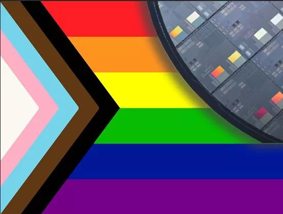
What does it mean to identify as LGBTQIA+ in the semiconductor industry? It’s an interesting question to ask, but a difficult one to answer. Because we live in a world in which cisgender heteronormity is assumed, it’s possible to self-identify as LGBTQIA+ without sharing that information publicly. Coworkers and managers might not even realize that their colleague or employee is gay, lesbian, transgender, non-binary or other. Unlike other minorities, notably people of color, LGBTQIA+ people may choose to keep their identities invisible.As I began outreach for this article, I recognized that some people might not want to expose a potential vulnerability to both their co-workers and a broader global audience of SEMI members, so I tried to make them feel more comfortable. I told them I’m a lesbian. I said that I’d send content for their review before publishing. But I quickly discovered that wasn’t enough, despite sweeping cultural and legal advances around LGBTQIA+ attitudes and identity. According to a 2020 Gallup Poll, 5.6% of U.S. adults now identify as LGBTQIA+, up from 4.5% just three years ago. In 2004, Massachusetts became the first U.S. state to legalize same-sex marriage, and in 2015, the U.S. Supreme Court made same-sex marriage legal in all 50 states. The semiconductor industry has been historically conservative. The times, however, are changing. Large chip companies such as AMD, Intel and Lam Research actively support diversity and inclusion efforts across minority groups, including LGBTQIA+, and that’s a good thing, but is it enough? And if not, what actions can SEMI members take to help LGBTQIA+ people in semiconductors feel safe enough to choose visibility?According to Antoinette Hamilton, global head of Inclusion and Diversity at Lam Research, more than 46% of LGBTQIA+ employees in the industry aren’t out in the workplace. That tells us there’s still work to be done, a challenge that Lam is embracing. With its Pride employee resource group (ERG) leading the way, partnerships with organizations such as PFLAG and Out Equal, and recruitment efforts made through organizations such as Out in Science, Technology, Engineering, and Mathematics (oSTEM), Lam has earned a score of 100 on the Human Rights Campaign Foundation’s Corporate Equality Index and was named one of the Best Places to Work for LGBTQ Equality.“At Lam, we understand the importance of empowering employees to bring their authentic self to work,” says Hamilton. “We believe when employees feel valued and included, each person can reach their full potential.”Back in 1992 when Intel paid to relocate Judi Goldstein, her partner and their son from New Jersey to Oregon, mainstream cultural attitudes toward gays and lesbians were very different. According to a June 1992 Gallup poll, only 48% of Americans thought that “gay or lesbian relations between consenting adults should be legal,” with 44% saying they should be illegal. A May 2020 Gallup poll recorded a dramatic shift in attitudes, with 72% affirming the legality of same-sex relations and only 24% opposed.By the late 1990s, Intel had extended domestic partner benefits to same-sex couples. “I registered my partner – now my wife – and our son, and realized that from then on, my whole family would have health insurance through Intel,” says Goldstein, who identifies as a gay woman and uses she/her pronouns. “Both relocating my family and providing family health coverage solidified my attachment to Intel, which was way ahead of other companies at the time.”By 1995, Goldstein became one of the first members of IGLOBE, Intel’s ERG for LGBTQ+ employees. Since that time, she’s observed further progress at Intel, first with the addition of gender identity and expression to Intel’s anti-harassment policy, and later with the inclusion of gender-neutral bathrooms at all major US sites. And advancement didn’t stop there.“We now have international IGLOBE chapters, a celebration of Pride Month in June, company support for the Equality Act and other legislation, a provision for transgender health benefits, and the launch of Self-ID efforts in 2017,” she says.From her start as software engineer more than 32 years ago to her current positions as director of the Open Source Audio and Security Engineering teams, Goldstein has played an instrumental role pioneering new technologies and mentoring other engineers at Intel – in addition to serving as a role model for LGBTQIA+ employees coming through the ranks. Now a grandmother with a five-year-old granddaughter, Goldstein lives in Oregon with her wife of more than 30 and two dogs. Location, Location, LocationAs social animals, we tend to value safe and welcoming places to live. When you’re LGBTQIA+, this may mean moving to an urban area that is more likely to embrace diverse orientations and cultures.After getting his master’s in astrophysics, Chuck Chung had a decision to make. Remain in the same field, which would limit his options on where to live, or get a doctorate in engineering, which would expand them.“In the ‘90s when I was making this choice, things were very different, and I knew that where I worked and lived would have a huge impact on how open I could be,” said Chung. “While I would have loved a career in astrophysics, I realized that engineering would be a more practical choice because I was more likely to find work in a city.”Both personally and professionally, engineering has proved a good choice for Chung. He’s lived in San Francisco and Silicon Valley for the past 18 years, where being out in the workplace is rarely an issue. “I compartmentalize my personal and professional lives when necessary, such as when business colleagues who are overseas talk about their families in casual conversation. Most of the time, though, my identity as a gay man is a non-issue, and I work for a company that really cares.”From his pioneering work in MEMS and genetic sequencing to his current focus on the next generation of microarchitectures at IBM, Chung has long thrived. Now, with a new book on MEMS Product Development – co-authored with two other Ph.D.’s, Alissa Fitzgerald and Carolyn White of A.M. Fitzgerald Associates – the best days of Chung’s career may still be ahead of him. He lives in the Bay area with his husband and their two children.Kunal Garg’s identity didn’t influence his career choices because when he started in semiconductors, he wasn’t out to himself or others. A few years into his engineering career at his former company, Garg realized his identity as a gay man at a time when the national discussion about same-sex marriage was at its apex – leading to some uncomfortable situations at work. “As some of my colleagues and managers openly debated same-sex marriage, they seemed oblivious to the fact that there were LGBTQIA+ people at work,” says Garg. “I knew then that I wanted to steer such conversations in a way that would feel safe and inviting for people like me, who work in this industry while being true to their identities.”Once he’d come out to his family and friends, particularly after he married his husband, Garg wasn’t willing to stay silent at work. “Although it took courage and internal struggle to come out to colleagues, my identity as a gay man wasn’t something I wanted to hide or deny anymore,” he says. “Some people laughed when I mentioned my ‘husband.’ The idea that their colleague, an engineer, an Indian immigrant, a man, could be gay and married to another guy was so foreign, it was almost laughable. Luckily, this didn’t stop me from being myself at work, and over time, these types of conversations became very rare.”Nonetheless, Garg looked around for ways to be part of the LGBTQIA+ engineering community. When he moved to AMD in Austin, he wanted to start with a clean slate. “When my manager called to invite me to join his team at AMD, I casually brought up the fact that my husband was going to need to start looking for a new job in Austin. And, very casually, he asked me what my husband did for a living, and we went on to discuss how Austin would be a great city for us to live in,” says Garg. “The fact that this was such a normal conversation was a big factor in my decision to join AMD.”Soon after starting as a design engineer at AMD, Garg found that LGBTQIA+ engineering community for which he’d been searching. He joined AMD’s Pride ERG, a group that he now chairs. “Being a part of this ERG has been transformational for me on a personal level and has allowed me to connect with my fellow engineers and people in my industry, beyond our mutual love for science and technology.”Become a change agentWhile some chip companies actively promote inclusion and diversity of LGBTQIA+ employees, others still have a long way to go. SEMI and the SEMI Foundation are uniquely positioned to help advance LGBTQIA+ equity issues in the microelectronics industry. "The SEMI Foundation is committed to promoting Diversity, Equity, and Inclusion (DEI) in our industry for the benefit of our workers and our member companies,” says Shari Liss, executive director of the SEMI Foundation. “We are designing programs for human resources departments, company leaders, and DEI allies to make the case for stronger DEI practices that will attract, retain, and promote LGBTQIA+ individuals and other underrepresented groups in our industry. We will soon publish SEMI's Roadmap to Diversity, Equity, and Inclusion and DEI Toolkit, which will contain tools to help companies strengthen their workplace cultures so everyone – including those that identify as LGBTQIA+ – will feel welcome, and will be able to do their best work."“If we want to truly see the semiconductor industry flourish on a global level, we need to push for equitable treatment of LGBTQIA+ and other minority employees,” says Garg. “SEMI can help by educating industry leaders, especially in countries outside North America and Europe, on how diversity and inclusion through policy are vital to their sustained productivity. These workshops and trainings should be data-driven to encourage companies to hire more LGBTQIA+ employees and to create policies that promote the well-being of all employees.”It’s not just at the company level or the industry association level that matters. Just as individuals are necessary change agents in proliferating greater equity among women and people of color, they’re also needed as allies of LGBTQIA+ people.“Like so many of us, I’d love to wave a magic wand to end discrimination based on gender identity or sexual orientation, but like any cultural shift, most change comes in small steps, not in giant leaps,” said Karen Lightman, executive director, Metro21: Smart Cities Institute – Carnegie Mellon University. “Fortunately, it’s easy to help make those small steps by becoming an ally to LGBTQIA+-identified people. When you see an injustice, don’t stay silent. Use your voice. There’s transformative power in that act alone. As one step, I’ve started using my pronouns when I introduce myself and now include them in my digital signature. It’s an easy way for me to express that I am an ally to LGBTQIA+-identified people.”Help us make the change. Use your voice. Get involved. Encourage your company to advocate for LGBTQIA+ inclusion and diversity.Maria Vetrano, principal of Vetrano Communications, is a PR consultant at SEMI Foundation.
Read More
Adnan Hamid, CEO, founder and visionary of Breker Verification Systems, an ESD Alliance member based in San Jose, Calif., once described his job in chip design verification at AMD as “breaking things.” When it came to naming his startup, Breaker was a natural choice. After some consideration, the “a” was dropped and the company became Breker. Now Hamid is breaking the most complex semiconductor designs and Breker, moving from a startup to a scale-up company, is a noted part of the functional verification space. Smith: Why does verification continue to take the most amount of time in a project cycle? Hamid: The project cycle for semiconductor design has changed. Design abstraction has been raised to a much higher level than the days when developers were connecting logic gates. Today’s developers are typing functions that don’t include lower-level implementation details. Designs incorporate more blocks of reusable IP. Both reduce design time. Meanwhile, designs are getting bigger with more blocks of IP stitched together, all in need of testing. As design complexity grows, the amount of testing and verification increases as a square of design effort. One block requires one functional verification effort. Four blocks of IP mean up to 16 functional interactions require verification. While design is moving up the abstraction level, that’s not the case for verification, where plenty of detail must be reimplemented. Verification has certainly evolved, but engineers still think at the level of independent stimulus, response and coverage, driving the need to allocate so much time for verification. Smith: Are chips targeting artificial intelligence and machine learning applications more difficult to verify? If so, why? Hamid: Yes, absolutely and it’s an interesting challenge, especially given that machine learning is based on massively connected processing element arrays. Attempting to verify the individual processing elements and the critical interconnects is complex. AI device arrays and, interestingly, verification test content operation may both be thought of as a mathematical graph of processing elements and interconnect. Their operation involves walking through the graph form to generate a result. Finding the optimum path through these arrays is key. To understand how these systems may be effectively verified, it is worth investigating planning algorithms. Originally proposed by IBM, these hold the key to this type of verification process. The AI- style algorithm starts backward at the end of the processing element array and tracks down the most optimal and likely paths through it. At Breker, we have used these planning algorithms extensively to drive our graph-based test content synthesis process. Smith: Does system integration require verification? Hamid: Yes, it does. In the past, most functional verification has been performed at the block level. However, with the increase in more specialized SoCs, functionality is spread across multiple blocks, as well as the software running on the processors, driving full system-on-chip (SoC) functional verification. In addition, new requirements such as security and safety must be validated. A system-level infrastructure such as cache coherency and power domain execution has become more complex and these must also be tested. The new frontier in verification is ensuring a fully operational SoC. Of course, given the size of these SoCs, hardware-assisted verification such as emulation is essential, and porting tests from block simulations to SoC emulations has become a requirement. This porting process is problematic and this in turn has driven portable tests, giving rise to the idea behind Accellera’s Portable Stimulus Standard (PSS), of which Breker was a major participant. Indeed, some companies are taking this to the next level by composing their system-level testbench at the same time as they commence SoC architectural design, and then developing the hardware design, software design and test content all in parallel, in the so-called “shift-left” manner. Smith: Is “shift-left” a growing trend that are you seeing in verification? Hamid: Yes. Shift-left is taking hold in hardware and software design, giving way to an increase in early test content composition. Then as individual blocks are finished and connected, their verification is driven from this same test content, saving a significant amount of time and effort. This is a huge verification and test generation change that was inevitable given the increased time-to-market constraints and SoC complexity. Figure 1: Shift-left is ushering in the next generation of SoC verification. Source: Breker Smith: As an entrepreneur, what advice would you give someone founding a startup or thinking about starting one? Hamid: Do not take the attitude “Build it and they will come.” My best advice for an entrepreneur or fledgling entrepreneur is to solve a specific customer problem, however narrow it might seem. Including services as part of a product offering and developing partnerships with other vendors helps with this and turns your company into a solution provider not a product developer. This is essential for getting the right products to market on time and within budget, and then ultimately scaling them across the market. The ESD Alliance and Accellera are hosting a two-part webcast series on the work-from-home experience titled Remote Work, Remote Chip Design: Building Chips During a Pandemic. The first panel, Wednesday, June 9, at 9:00am PDT, will feature a discussion led by Tom Fitzpatrick, strategic verification architect from Siemens EDA verification engineers through their experiences converting their home offices into verification test labs. The second panel in July will explore how executives managed a remote workforce and explain how they plan to bring employees back to physical offices. About Bob Smith Robert (Bob) Smith is executive director of the ESD Alliance, a SEMI Technology Community. He is responsible for the management and operations of the ESD Alliance, an international association of companies providing goods and services throughout the semiconductor design ecosystem.
Read More
A change is underway in the manufacturing sector as the use of curvilinear shapes on photomasks grows, leading to the real possibility of curvilinear shapes in designs. It may just be the start of a revolution away from Manhattan or rectangular shapes to curvilinear shapes. Changing the physical design infrastructure to be curvilinear seems too daunting a task. Are curvilinear shapes in designs a real possibility? I turned to Aki Fujimura, CEO of D2S, a member of the ESD Alliance, a SEMI Technology Community, to further explain the shape of the future. Smith: What is the difference between Manhattan and curvilinear shapes? Fujimura: Manufactured masks and wafers are all curvilinear, even if the input CAD geometries are rectilinear (shown in Figure 1). It’s always been true that nature can’t make 90-degree turns, so sharp corners were always a matter of how closely you looked. These days, at the leading-edge nodes and their required resolutions, wafers and even masks are all visibly curvilinear as you can see in the graphic on the left in Figure 2. Since the 1980s, both chip design and chip manufacturing systems have used axis-aligned rectangles, or “Manhattan” geometries, because 1) that was sufficient to design transistors and interconnect for the most part, and 2) CPU-based computer algorithms can be made much more efficient for Manhattan geometries. Curvilinear shapes can be piecewise linear polygons of some resolution, or spline-like formats that are curvilinear at any resolution, or specific curved patterns like circles and ovals. Figure 1: All shapes on masks and wafers are curvilinear, even if the input geometries are Manhattan. Source: D2S Smith: What are the benefits of curvilinear masks? Fujimura: The manufacturing side of the semiconductor community knows that the best possible process window for wafer lithography is obtained by using curvilinear correction of mask shapes instead of Manhattan shapes. There have been numerous studies on the topic over several decades. The technique to generate purely curvilinear mask shapes is known as inverse lithography technology or ILT and is an advanced form of optical proximity correction (OPC). At a February 2020 eBeam Initiative event, Micron Technology presented a study showing process window improvement up to 85% for advanced memory designs as a result of using curvilinear ILT (shown in Figure 2). Additionally, Ryan Pearman from D2S presented a study at Photomask Japan 2019 showing that it is preferable to move toward a completely curvilinear paradigm, not only because ILT is better, but because the mask manufactured will have reduced variability. Figure 2: Micron Technology explained the benefits of curvilinear mask shapes for advanced memory at the eBeam Initiative event during 2020 SPIE Advanced Lithography Conference. Source: Micron Technology Smith: If the benefits have been known for decades, why is it happening only now? Fujimura: Several things happened at the same time. Multi-beam mask writing is now available. GPU acceleration for general computing has become mainstream. And wafer process window (resilience to manufacturing variation) is increasingly a problem for the leading-edge nodes as we are in the 5nm node, going to 3nm. Curvilinear ILT is needed much more now than before, will soon be needed for EUV lithography too, and is now possible because of multi-beam mask writing and GPU acceleration. Smith: Curvilinear mask shapes enable curvilinear design shapes too? Fujimura: Adoption of curvilinear mask shapes is the first step in targeting curvilinear shapes on wafers. Without curvilinear masks, it is difficult to target and reliably manufacture curvilinear designs. Curvilinear ILT works in the pixel-space to output the desired mask shape to maximize the process window for wafer lithography. A side effect of curvilinear ILT is that it can also take curvilinear targets as input. ILT, most likely GPU-accelerated ILT, works with rasterized input data, so the ILT algorithm itself is not affected even in runtime by having any amount of curvilinear design data. The resulting mask shapes are written in multi-beam mask writers, which write pixels with doses. They too will write curvilinear masks at the same speed as Manhattan masks. Suddenly now, curvilinear designs can be handled by chip manufacturing equally well for the first time in about 30 years. Smith: But curvilinear designs would be hard, right? There are a lot of tools that depend on the Manhattan assumption. Fujimura: Yes, you’re right. We’re not going to suddenly see chips that have curvilinear routing all over the place, or curvilinear intra-connect in standard cells or memory cells. The entire physical design infrastructure that includes place and route, timing, custom layout, parasitic extraction and design rule checking moving to curvilinear design all at once is extremely unlikely. Could portions of these problems be tackled for specific cases over time as “hot spot” solutions? With GPU-accelerated SPICE being available now, as an example, if GPU acceleration is adopted for design, the same transformation that happened in manufacturing can (gradually) happen in design too. The key question is whether it’s worth the trouble. Smith: Is it worth the trouble? Fujimura: I don’t know if it’s worth the trouble for the entire infrastructure. For hot spots, “hot” for various reasons, there are certainly benefits. Jogging a 32-bit bus by one grid is certainly much more economical space-wise with curvilinear shapes. Inside standard cells or memory cells, there are certain types of features that pack better with curvilinear designs. In general, interconnect is the limiter to chip size of course, but there are always critical areas that could use help to shrink. There are manufacturability benefits as well. In general, when something changes so drastically as this for the first time in 30 years, there’s bound to be some innovation that takes advantage of the discontinuity. Let’s see what the combined capitalistic power of the entire community might be able to come up with. The first thing is to let everyone know that curvilinear designs will be manufacturable today. Hear insights from other leading electronic system design industry CEOs at the SEMI ESD Alliance CEO Outlook on May 18, 2021, 2:00pm-3:00pm PDT. Panelists will discuss the state of the industry along with their views of the outlook for the coming years. Registration is free for SEMI members. About Bob Smith Robert (Bob) Smith is executive director of the ESD Alliance, a SEMI Technology Community. He is responsible for the management and operations of the ESD Alliance, an international association of companies providing goods and services throughout the semiconductor design ecosystem.
Read More
As we move through Q2 of 2021, it seems that the world is finally approaching normalcy. But I don’t believe our lives and businesses will ever be the same. Travel is unlikely to return to the same level as pre-COVID-19 for many years. I’m sure many companies will establish tighter travel policies and budgets as virtual conferencing has proven to be beneficial and cost-effective. Patients and doctors who were skeptical of telemedicine are embracing it, and although it’s not perfect, it has filled a needed gap. Online learning essentially happened over a weekend and will now be part of many curriculums and programs. All of these elements have spurred our semiconductor industry into a super cycle. Demand for chips is leading to an increased demand for semiconductor equipment. Semiconductor capital equipment expenditures in 2020 surpassed $63 billion and are forecast to top $70 billion in 2021. The secondary equipment market typically makes up about 5% to 10% of that. Our inquiries have definitely increased this year. With this in mind, I’d like to share some thoughts for the remainder of the year. Storage of Chipmaking Equipment Not New The semiconductor industry has been experiencing an equipment shortage for some time. It is difficult for original equipment manufacturers (OEMs) to support such a large variety of products and technologies. Some companies use equipment for manufacturing 150mm, 200mm and 300mm wafers. Fabs still run 30-year-old technology on 150mm wafers while the latest technology is manufactured on 300mm wafers. We’ve also seen new technologies like silicon carbide (SiC) being developed on these smaller wafer sizes. Unfortunately, some OEMs stopped making 150mm and 200mm some time ago and have only recently jumped back into the market. These OEMs have had to balance technological advances, pricing, and manufacturing capacity to meet this demand since their primary focus is on 300mm equipment. Third-party refurbished equipment suppliers have also experienced an increase in demand over the last several years. We see it increasing at all technology levels over the next three to five years. This translates to increased equipment pricing for both new and used equipment, as well as increased lead times. Growing Demand for Legacy Tools Many electronic products we use and are familiar with don't require state-of-the-art technology. For instance, cellphones, electric vehicles, wearables, monitors and industrial products still contain many chips manufactured on 200mm wafers using 200mm equipment. There are still approximately 200 200mm fabs worldwide and this makes up about 25% of all wafer capacity regardless of wafer size. These fabs manufacture analog devices, MEMS products, power management ICs, RF devices, discrete devices and sensors. We have also seen an increase in lead times for 200mm equipment. Typical lead times of three to six months have increased in some cases to one year or more. This situation has created a dramatic increase in chip making equipment prices and we do not expect much relief there. Many OEMs transitioned to 300mm equipment prior to 2010. Revenue and profit margins are much higher for them on 300mm equipment. 200mm manufacturing was supported by many third parties for a while. However, in 2016 we saw a resurgence in 200mm equipment, and at that time many OEMs began jump-starting their supply chains. It took some time for them to develop new supply chains, upgrade technology and in some cases hire newly trained engineers to support these new tool sets. All this costs money, which is why we will continue to see an increase in new legacy equipment pricing. Because manufacturers and products may not be able to support these prices, we expect the robust third-party ecosystem to continue. SurplusGLOBAL's Response to this Demand One of the advantages we bring to the secondary equipment market is our ability to recycle technology. We continuously search for opportunities to purchase large packages of tools from companies that are transitioning technology nodes, moving from 200mm to 300mm wafer size or changing product lines. We spend approximately $65 million to $100 million each year on purchasing equipment and in some cases storing it for the right customer. For instance, a memory company may be changing technology nodes and no longer needs its equipment. This use to happen on a predictable schedule. Instead of scrapping that equipment, SurplusGLOBAL purchases and stores it. Sometimes we only need to store it for one month before relocating it. However, in many cases, we store it for one year or more. We may power it on at a later date if it is in good condition. In some cases, we work with an OEM or third party to have it refurbished and ready for a new customer. In response to the need for more secondary market equipment, we have opened up additional offices in Japan and Singapore to stay close to and better support our customers in those regions. Finally, our biggest and most recent endeavor is building our Semiconductor Equipment Cluster, which opens in July 2021. Learn more about the SurplusGLOBAL Semiconductor Equipment Cluster. Emerald Greig is executive vice president Americas at SurplusGLOBAL.
Read More
As the global economy is constantly transformed, the need for new skills has never been higher. The microelectronics industry is thoroughly affected by this urgent need. To develop a workforce fit for the future, it is crucial to invest not only in reskilling and upskilling, but also in skills anticipation and inclusivity. To tackle this need, the European microelectronics ecosystem has adopted many bottom-up initiatives and good practices supporting lifelong learning. Many companies collaborate with universities and training institutes to offer work-based training, and numerous events take place to support women participation in STEM and to attract more young talent to a microelectronics career. Despite these great efforts, further pooling of investments is necessary if Europe is to develop efficient lifelong learning programs. Creating strong skills partnerships is vital for sustainable upskilling and reskilling initiatives. According to the World Economic Forum (2021), greater private-public collaboration on large-scale upskilling and reskilling initiatives could boost global GDP by $6.5 trillion and lead to the creation of 5.3 million net new jobs by 2030. What is the Skills Partnership? Against this backdrop, SEMI Europe is launching the Skills Partnership for Microelectronics. The partnership brings together industrial and education partners from the microelectronics ecosystem to implement the Pact for Skills, an EU initiative which aims to boost upskilling and reskilling investments in key ecosystems for Europe’s competitiveness. Following the high-level roundtable with SEMI Europe’s Advisory Board, hosted by European Commissioners Thierry Breton and Nicolas Schmit, the microelectronics sector was selected in November 2020 as one of the key ecosystems for the first wave of implementation of the Pact, alongside automotive and aerospace/defense. Read more details about the October 2020 roundtable. 59 partners have already endorsed the Pact for Skills for Microelectronics. The Skills Partnership for Microelectronics aims to: Exchange good practices of upskilling and reskilling initiatives of the microelectronics industry Develop sustainable collaboration mechanisms that will monitor microelectronics skill needs, learning from the examples of the METIS blueprint project Promote the microelectronics sector as a career choice Boost the presence of women and other under-represented groups in the sector. The partners will have the opportunity to liaise not only with European, but also with national and regional authorities and clusters, so that a pan-European holistic approach to microelectronics skills development is achieved, and a significant flux of public and private investments on skills is mobilized. To launch this ambitious partnership, SEMI Europe held an initial workshop on March 17. Participants included representatives from the European Commission’s DG Connect, DG Employment and DG Grow, national and regional authorities, and over 70 industry and education partners. The workshop opened with representatives from the European Commission informing all stakeholders about the Pact for Skills initiative, as well as about EU skills-related funding opportunities. In the framework of the Pact for Skills, the Commission will support the ecosystems with a Networking Hub, a Knowledge Hub and a Guidance Resources Hub. These platforms will be available later in 2021 and will act as a one-stop-shop to support the partners and provide information on EU policies and funding opportunities. Other presentations went on to set the scene, presenting the main priorities of the partnership. Françoise Chombar, CEO of Melexis, highlighted the skills challenge experienced by the microelectronics industry. She emphasized the importance of lifelong learning and the danger of the gender disbalance in the sector and underlined the huge innovation potential and profitability that could be unleashed for Europe if the gender gap is successfully addressed. Moreover, the preliminary results of the METIS Microelectronics Skills Strategy were presented, to offer the basis for the partnership’s approach to skills anticipation. The partnership will establish working groups that will investigate the industry needs, leading to a better connection with the offer of education and training programs. Last but not least, the partnership aims to promote national and regional funding of upskilling and reskilling initiatives. In this regard, representatives from national and regional authorities and clusters participated in the meeting. The government of the Basque region had an active role, presenting the region’s priorities, incentives and main actions on promotion of lifelong learning initiatives. The next steps The meeting concluded with an overview of the next steps for the newly launched partnership. In the next workshop, the partners will align on the specific KPIs, as well as on the focus areas where they would like to engage (skills anticipation in semiconductor manufacturing, skills anticipation in semiconductor design, gender balance, etc.). In that framework, the executive board will be established, as well as the working groups that will lead the work of the partnership and set targeted objectives. If you want to take active part in the creation of this large-scale initiative, please fill in your details here. To learn more about the initiative, click here or contact [email protected]. Stefania Gavra is public affairs manager at SEMI Europe.
Read More
As we pass the work-from-home one-year mark, most of us still work remotely and will do so for the foreseeable future. As live trade shows and technical conferences were cancelled one after the other, virtual events became the norm. And, teleconferencing became a way of life. While possibly overstating our role, we have the semiconductor industry – from system design through manufacturing and system integration – to thank for a long history of achievement that made the transition to working remotely relatively seamless and straightforward. The shift, in some cases, took some time to sort out as we set up a workable home office, moved to video conferencing with intermittent connections and settled into a routine. Nonetheless, many of us became more productive and, in some cases, even too productive. Each spoke in the global electronic products hub contributed through creativity and innovation with a pinch of ingenuity and grit. Of course, we could have worked remotely 10 years ago, but not nearly as efficiently. Over the last 10 years, the economy moved to the cloud, producing new opportunities across the global market. Many of these opportunities were made possible by the electronic system supply chain and combination of semiconductor technology, electronic product innovation and people who figured how to leverage it with software platforms to tie it together. Zoom, one of our teleconferencing lifelines, is a good example, as are Netflix, our ongoing source of entertainment, and Roblox, a platform to build games. Facebook, Twitter, LinkedIn and the like sourced the news for us and kept us in touch. Amazon delivered our online purchases and GrubHub brought us our takeout dinners. All rely on cloud computing with thanks to the semiconductor industry. Another great example are data centers powered by semiconductors and the amount of data they processed last year. According to International Data Corporation (IDC), 64.2 zettabyte (ZB) of data was created or replicated due to the dramatic increase in the number of people working, learning and entertaining themselves from home. (Its revised model for global data creation and replication predicts the CAGR will grow to 23% over the 2020-2025 forecast period, a sure bet that the semiconductor industry will address ways to manage the growth, possibly through new AI chips.) Our connectivity is driven by smartphones optimized for low power and the performance of more complex chips. Over the last 10 years, design tools have been enhanced and new methodologies have been introduced to respond to the needs of the increasing complex chips for applications that demand high bandwidth, low latency and reduced power consumption and area. Manufacturing is retooling for higher automation under smart manufacturing initiatives and packaging is even more sophisticated with increasing integration and the 2.5D and 3D packaging rollouts. Let’s take stock of our success. The semiconductor industry has a storied tradition of breakthrough technology since its inception. The consumer electronic product craze started when the first PCs were rolled out in 1971, notes the Computer History Museum. Primitive laptops that followed in 1986 gave way to notebooks in 2007 and the ubiquitous smartphone in 2002 – and the rocket fuel for much of this was the buildout of computer networks, hyperscale datacenters and the cloud. Nothing’s been the same since. The next time we turn on our laptop, click on the link for the latest teleconference from our remote home office in comfortable sweats sitting in our ergonomic chair, let’s take a minute to acknowledge our industry’s grand achievement. And, thank one and all for their contribution and consider what’s coming next. About the Author Robert (Bob) Smith is Executive Director of the ESD Alliance, a SEMI Strategic Association Partner. He is responsible for the management and operations of the ESD Alliance, an international association of companies providing goods and services throughout the semiconductor design ecosystem.
Read More
At the SEMI Foundation, we’re taking steps to support a big, audacious goal – achieving gender parity in the microelectronics industry. Dating to its roots at Bell Labs, Fairchild Semiconductor, and Intel in the late 1950s and 1960s, the semiconductor industry was pioneered by men at a time when far fewer women were in the workforce. While women have made major workforce gains since those early days, we’re still far from achieving anything close to an equitable representation of women. According to the U.S. Bureau of Labor, only 11.8% of electrical and electronics engineers – and just 8.7% of mechanical engineers – are women. What’s more, research from the American Association of University Women (AAUW), a non-profit that champions equity for women and girls through advocacy, education, and research, tells us that women drop out of engineering careers more steadily and quickly than men. According to AAUW research, just 30% of women working in engineering are still in the field after 20 years compared to 35% of men. By the time women have been in the field for 30-34 years, that number falls to 19% – while it increases to 39% of men among the same cohort. The small number of women in engineering careers and the fewer still who stay in engineering long term illustrate the troubling gender disparities in the industry. Even with these low numbers, however, there are still women who have managed to not just stay in the industry, but to thrive and lead within it. I talked with four of these women about their professional journeys and how they believe women can be best supported in careers in our industry. The AAUW research report Solving the Equation: The Variables for Women’s Success in Engineering and Computing shows that attrition in engineering is higher among women than men. Passion for math and scienceLam Research VP Gowri Kamarthy took her Ph.D. in chemical engineering from UC Berkeley directly to Lam Research, where she’s spent the past 22 years in technical positions. Today she heads the company’s conductor etch product line.Coming from a family of engineers, including her father and siblings, Dr. Kamarthy had a built-in support system that was essential to her success. She never felt intimidated by male peers after spending her formative years pursuing her passion for math and science.“I may have stood out as a minority in the field of engineering, but there was also a silver lining in standing out,” she said. “People notice you.”Kamarthy realizes that engineering careers are generally perceived as being less compatible with family life, for both women and men.“Anyone who wants work-life balance in an engineering career will have to navigate its special challenges, including the need to work long hours to match the rapid pace of innovation,” Kamarthy said.Drawing from her own experience, Kamarthy offers some career advice. “Perseverance and grit are key to success,” she said. “The other ingredient is luck. I was fortunate to have great bosses at Lam who didn’t see gender first and foremost. Instead, they recognized my ability to deliver on projects and encouraged me to perform at my best.” A love for math and science. The confidence to excel in those subjects. A support system to help her through the bumpy times. These were also truths for Sandy Vos, Ph.D., director of R D at NXP Semiconductors.“I was always good at figuring things out,” says Dr. Vos. “I remember feeling enthralled when I got my first internship because it combined engineering, math, science and manufacturing.” Like Kamarthy, Vos was aware of her status as a woman in a male-dominated field, but it didn’t stop her.“If anything, my gender drove me to prove myself,” Vos said. “And I’ve been fortunate because everywhere I’ve worked, I’ve been a part of a smart and collaborative team.”That doesn’t mean gender never came into play. Whenever it did become an issue, Vos didn’t shy away from hard conversations. She recalls having a conflict on the plant floor with two men who each stood over six feet and were about 100 pounds heavier.“I had a conversation with them, and we figured it out,” she said. “But for a while there, my heart was racing.”Gender felt like a bigger issue when Vos was younger. “Now that I have gray hair, it’s not much of a concern,” Vos said. “But earlier in my career, I started putting Ph.D. on my business card so people would know I could talk technical details.”Though just one of three women in an undergraduate class of 35 engineering students – and with a teaching cohort of all-male professors – Debbie Gustafson anticipated equitable treatment in her college engineering program. She had the same outlook when she began her career in semiconductor manufacturing. But the belief that she’d receive the same treatment as her male peers went largely unfulfilled. This didn’t slow her down. During her first year as CEO of Energetiq, she grew the company’s revenues and valuation. A year later, she steered the company through a successful acquisition by Hamamatsu Photonics. Today Gustafson continues to lead Energetiq as a wholly owned subsidiary, but the road to the top job wasn’t without hurdles. Gustafson muscled through the tough times.“When I started out, I traveled to Japan and Korea when there weren’t other women in technical roles,” she said. “My first meetings were extremely frustrating. I was the only woman in the room, and the men wouldn’t address me. This went on for a year, but I kept coming back and built the relationships.”Now a member of the SEMI Foundation Board of Trustees, Gustafson credits mentors with helping her navigate the nuances of doing business across cultures during those early years.A rocket scientist among usAlissa Fitzgerald might tell you that MEMS isn’t rocket science. But that’s only because she has a Ph.D. in Aeronautics and Astronautics, which actually is rocket science. Dr. Fitzgerald worked at a government laboratory and a large defense contractor before she got her Ph.D. and moved to a MEMS industry startup. Though gaining valuable experience, she found the environments too hierarchical and lacking in career development opportunities for young female engineers. As one of the few women engineers at these heavy-duty engineering firms where, in the 1990’s, there were no women in leadership roles, Dr. Fitzgerald sensed that opportunities for her to advance were remote. Fitzgerald started her own firm rather than climb up the ladder of another company, but it turns out, her motivation had nothing to do with gender.“It was the way engineers were treated like Dilbert,” she said. “I felt like a cog in the wheel, working for corporations that weren’t nurturing or appreciative of engineers.”After years of working for other companies, Fitzgerald founded the eponymous AMFitzgerald Associates, a developer of innovative MEMS and sensor solutions for specialty applications. When gender did come up for Fitzgerald, it manifested in men questioning her technical abilities.“Early in my career, I felt like I had to prove myself worthy, even though my degrees were from MIT and Stanford,” she said.Over 3,000 respondents to the Workplace Experiences Survey, sponsored by the Society of Women Engineers and the Center for WorkLife Law at UC Hastings Law, validate Fitzgerald’s experience. 61% of women vs. 35.1% of white men surveyed cited Prove-It-Again Bias – “having to prove themselves repeatedly to get the same levels of respect and recognition as their colleagues.” For engineers of color, that disparity was even worse. 68% of engineers of color (both women and men) reported Prove-It-Again Bias vs. 35% of white men.“For women and people of color, there’s rarely an assumption of competence,” Fitzgerald said.It’s sad but true that we can’t decouple the challenges women face from the challenges people of color face. Both are dramatically underrepresented as chip companies, and women of color represent the smallest percentage of the industry’s workforce and leadership.Inclusivity mattersWorking toward gender equity isn’t just a case of doing what’s right. It’s a case of doing what’s profitable. Research shows that companies with more women on the board perform better.“Given the pace of innovation in semiconductors, we need people from different backgrounds and perspectives to solve the hard problems challenging our industry,” Kamarthy said.Vos appreciates the fact that SEMI is creating a forum of inclusion.“Inclusion starts when you’re young,” she said. “School-aged kids are already making decisions about a future they see as exciting and possible. Our job is to make sure they have the opportunities to pursue what they envision.”Change won’t come magically, though. Fitzgerald believes companies need to make a concerted effort to attract a diverse population.“While I see a disproportionate number of female applicants, I’m more the exception than the rule,” she said. “When male executives call and ask, ‘How are you finding all these amazing female engineers?’ I say, ‘they’re finding me.’”Elevate the storyAchieving gender parity in microelectronics is a daunting task. Fortunately, access to SEMI’s global membership puts us in a unique position to make this deeply complex story clear and relevant to our members, so we can help support the shift.We’re looking at both the stark numbers of women working in microelectronics and at the lack of longevity of women in engineering. We’re elevating the conversation about childhood education. Why are girls passed over in math and science classes in early grade school, and what is the effect of teachers’ lowered expectations for girls taking these classes? What does it mean to be the only in the room? The only woman, or the only woman of color, on a team or in a meeting room. Feelings of isolation or disengagement – or frustration with Prove-It-Again bias – often lead to turnover in an industry that already struggles with retention.Reverse the trendThere’s much SEMI members can do to work toward gender parity in our industry. Look at recruitment, hiring, retention and promotion processes to see how women fare in them. Consider how to create a company culture of self-awareness and inclusion. Ensure equitable pay. Suggest and request women speakers for keynotes and panels at conferences. And offer workplace flexibility to allow women – who often bear most family responsibilities – to take time off or reconfigure schedules so they can help care for children or ailing parents.It’s time for our industry to reverse the trend of gender inequality. Research shows that companies with greater gender and racial parity are more productive, innovative, and profitable. If we welcome and support women in our companies, we will help women – and our industry – reach their full potential.Get involved with SEMIRegister for the Women in Semiconductors (May 3, 2021). This virtual event will include interactive exploration and discussion on strengthening the roles of women in hybrid and remote work environments. Everyone managing teams or experiencing the gender parity challenges and opportunities will benefit from the fresh thinking and best practices that the Women in Semiconductor program is known for.Participate in the SEMI Mentoring Program. By matching mentees with industry leaders and professionals, SEMI Foundation facilitates one-on-one mentoring relationships that benefit all participants. Whether you are a recent university graduate or growing in your microelectronics career and looking for support, participating in the SEMI Mentoring Program will put you on the right track.Participate in the McKinsey Company 2021 Women in the Workplace Study, which looks at representation and the experience of women in companies across the U.S. and offers recommendations on how to retain and support women. Email [email protected]. Shari Liss is executive director of SEMI Foundation. Connect with her on LinkedIn.
Read More
MEMS actuators transform electronic signals into something that can be sensed or touched by the end user of an electronics device. A case in point: MEMS actuators such as print heads in inkjet printers transform electronic files into text or beautiful images. In 3D printers, actuators can produce real objects. Inside smart glasses, tiny MEMS mirrors can create virtual objects. Little surprise, then, that integrating these powerful devices into the end products is a multidisciplinary enterprise. STMicroelectronics has been successfully leading the deployment of dedicated MEMS actuator solutions with customer products in various market segments. SEMI spoke with Anton Hofmeister, group vice president and general manager of the MEMS Actuator Division at STMicroelectronics, about MEMS actuator trends. Hofmeister shared his views at the SEMI MEMS Imaging Sensors Forum as part of the virtual SEMI Technology Unites Global Summit. Watch the STMicroelectronics’ presentation on-demand until March 26, 2021. Registration is open. SEMI: What is the difference between MEMS devices that sense and MEMS devices that actuate? Hofmeister: MEMS sensors gather data from the world around us including motion, pressure and air temperature and transform them into an electrical signal. Actuators work the other way round. They receive an electrical signal and transform it into some well-controlled actuation such as ejecting a fluid, moving a membrane or deflecting a laser beam. SEMI: How can MEMS actuators’ integration be simplified to be embedded in new applications so they appeal to consumers? Hofmeister: The challenge of integrating MEMS sensors into devices has been simplified by demo kits and evaluation boards, which customers use to embed the sensor into a system. MEMS actuators are more difficult to integrate. They often power the core function of a system and therefore require deep system understanding. Reference designs are a big step forward in simplifying integration. My presentation at the SEMI MEMS Imaging Sensors Forum showcased some examples. MEMS micro-mirror projection for augmented reality (AR) glasses is an example of a complex system that requires multiple types of components to function. Together with several partners, STMicroelectronics recently announced the LaSAR Alliance, which will develop reference designs to enable the AR glasses market. SEMI: MEMS sensors and actuators are considered the backbone of many consumer products. Are MEMS actuators also mostly used in automotive? Hofmeister: The widest use of MEMS actuators has so far been in print heads for inkjet printers. In recent years, we have seen actuators adopted in emerging applications ranging from piezo heads for 3D printers to MEMS mirrors for laser beam scanning systems or 3D sensing solutions for consumer applications. The first high-volume application in automotive will likely be MEMS mirrors for LIDAR systems. SEMI: What market growth trends do you see for MEMS sensors and actuators? Hofmeister: The sensorization trend, which aims to collect data from homes, cities, factories, cars and personal devices, continues to drive the adoption of sensors and actuators for a wide variety of applications. While the last wave of MEMS growth was triggered by one end product – the smartphone – the next wave will be driven by multiple applications and use cases in industrial, medical, automotive and personal electronics. SEMI: How can technology unite us? Hofmeister: In recent months, we have all experienced vividly how vital technology has become. MEMS, and semiconductors in general, are an integral part of many products and services that make our lives easier. Communications technologies have been particularly important during this pandemic, whether using the personal devices as our interface to the digital world or the complex infrastructure that they operate through. I hope that my participation at the summit helped increase awareness of the new possibilities and opportunities that technologies like MEMS actuators have to offer to create products and services that further improve people’s lives. Anton Hofmeister is group vice president at STMicroelectronics, general manager of the company’s MEMS Actuator Division and managing director of its German subsidiaries. Hofmeister has been with STMicroelectronics for more than 30 years, working in Germany, France, the U.S. and Italy. He has held managerial positions in key account management, product and strategic marketing, advanced R D and general management. For the past 10 years, he has managed various product divisions in the MEMS sector. Hofmeister has also served as a board member of the Singapore-based molecular diagnostics company Veredus Laboratories. Serena Brischetto is senior manager of Marketing and Digital Engagement at SEMI Europe.
Read More
With each transition to a new technology node, fab requirements for metal and particle contamination become more stringent, posing challenges for existing coating methods such as anodization or plasma spray that may not provide complete protection against contamination especially on critical chamber components with complex geometry. SEMI spoke with Beneq business executive Sami Sneck about common metal and particle contamination issues with critical chamber components, coating methods to protect against corrosion, and properties to look for when selecting the optimal protective coating solution. Sneck discussed the unique benefits of atomic layer deposition (ALD)anti-corrosion coatings with Aluminiumoxide (Al2O3) and Yttrium Oxide (Y2O3) and offered recommendations on how to work with original equipment manufacturer (OEM) partners to design, test and implement an ALD coating solution for semiconductor equipment. To learn more, visit Beneq at its digital booth at SEMI Technology Unites Global Summit, available on-demand until March 26, 2021. Registration is open. SEMI: How does ALD compare with other coating methods such as anodization and plasma spray? Sneck: ALD enables conformal dense and pinhole-free coatings on complex shapes. We can deposit various ALD coating materials on parts made of various materials. All other coating techniques have limitations. For instance, anodization is conformal, but porous and is suitable for Al2O3 used for aluminum parts. Plasma Spray is a line-of-sight method and not conformal on complex shapes, such as holes in showerhead parts. SEMI: Which substrate materials work for ALD coatings? Sneck: In general, parts made of common metal materials, such as aluminum, stainless steel or titanium, all work well with ALD coatings. Commonly used ceramic materials work well with ALD too. Plastic materials need to be coated generally at a lower temperature, which limits the coating material selection, but materials such as Al2O3 can be applied as well. SEMI: What is the maximum coating thickness you can reach with ALD? Does this depend on the material? Sneck: Yes, indeed. The maximum coating thickness does depend on the material of the part that we are coating. Polymer materials for example, have a very large coefficient of thermal expansion, which limits the practical coating thickness to the 100-nanometer level. On metal and ceramic parts, coatings of several micrometers are possible too. Typically, ALD coating thickness on chamber components range from a few hundred nanometers to one micrometer. SEMI: Which aspect ratio can you coat with ALD? Sneck: Basically, ALD can coat aspect ratios of 1000:1, but this would be extremely slow. In practice, some of the most complex parts are showerhead parts with small holes. Typically, these have an aspect ratio of around 100:1, which is perfectly commercially feasible for ALD. An extreme example would be gas lines: In this case, the aspect ratio may be also around 100:1, but the physical distance from one end to the middle may be half a meter. In this respect, it is not practical to wait for gas diffusion to reach such a depth level. Instead, the gas lines can be coated by forcing the ALD precursor gas flow into the gas line parts. This works well but needs part-specific manifolds to guide the gases. SEMI: What is the lifetime of ALD coating compared to other coatings? Sneck: ALD coatings differ from other coatings a couple of ways. First of all, ALD coatings generate less particle contamination since they are non-porous. Secondly, and most importantly, ALD coatings can cover areas that other coatings cannot. What is considered the lifetime of a certain part depends on various factors. Ultimately, the lifetime needs to be confirmed by testing parts in actual process chambers by running a lot of wafers through the chamber and monitoring critical parameters such as particle level and yield. SEMI: If you have multiple shelves with parts in the reaction chamber, how does the shelf position affect the coating uniformity? Is center shelf better than top and bottom shelf? Sneck: Uniformity depends on many parameters, including the part geometry, part holder geometry, batch size and coating material. When the shelves supporting the parts are optimally designed and the gas flow is well-distributed to all shelves, all shelves from top to bottom show similar uniformity. SEMI: Is there any risk of cross-contamination? Sneck: Cross-contamination could potentially be caused by the parts themselves or by different coating materials. The batch setup is fixed in production use, which means the parts are the same in every batch. The only variation is that the batch may not be full in some cases, but then we do not fill the empty part of the batch with other parts that could cause contamination in order to prevent contamination from one part type to another. Cross-contamination from one coating material to another is not a usual concern but can be prevented by using dedicated reaction chambers for different coating materials. This is very easy to do with Beneq P800. Sami Sneck manages Beneq’s semiconductor part coating business. He joined Beneq in 2005 and since then has held various professional and management positions including product manager, application manager, director of ALD group, head of sales, and head of Asia. He earned his MSc degree in Chemical Engineering in 2001 from Helsinki University of Technology. Sneck has special expertise in Atomic Layer Deposition technology and business development. He has played a vital role in introducing various ALD production concepts and solutions to several industries ranging from jewelry to photovoltaics, electronics and semiconductors. Access the free webinar recording and discover the latest anti-corrosion coating solutions and the unique benefits of ALD (atomic layer deposition). This webinar is particularly helpful for process engineers, equipment engineers and others responsible for contamination control and equipment yield. Serena Brischetto is senior manager of Marketing and Digital Engagement at SEMI Europe.
Read More