downloadGroupGroupnoun_press release_995423_000000 copyGroupnoun_Feed_96767_000000Group 19noun_pictures_1817522_000000Member company iconResource item iconStore item iconGroup 19Group 19noun_Photo_2085192_000000 Copynoun_presentation_2096081_000000Group 19Group Copy 7noun_webinar_692730_000000Path
Skip to main content
Default Banner Image

semiconductor industry

ULVAC Technologies’ David Mount is working with The CIA. Is he the Jack Reacher of the MEMS and sensors industry, jetting around the world to secret meetings, you wonder? While David isn’t quite the super-spy that you might have imagined, he is doing some fascinating work on behalf of ULVAC Technologies, the world leader in vacuum technology.ULVAC has been collaborating with The Culinary Institute of America (CIA) on Menus of Change, “a ground-breaking initiative from The Culinary Institute of America and Harvard T.H. Chan School of Public Health that works to realize a long-term, practical vision integrating optimal nutrition and public health, environmental stewardship and restoration, and social responsibility concerns within the food service industry and the culinary profession.”ULVAC also partners with Menus of Change (MOC) University Research Collaborative, a group of elite universities and food-service executives working together to “accelerate efforts to move Americans toward healthier, more sustainable, plant-forward diets.” MEMS Sensors Industry Group’s Nishita Rao caught up with David, a featured speaker at MEMS Sensors Executive Congress on October 29-30, 2018, in Napa, Calif. to give MSEC attendees a preview of David’s talk. SEMI: How did ULVAC get involved with The CIA on Menus of Change?Mount: People in the MEMS sensors industry may not know that ULVAC started as an equipment supplier to the food industry. In 1952 ULVAC began supplying freeze-drying equipment – which relies on vacuum technology — to food companies tasked with providing long-lasting foods and beverages for the U.S. military under the Marshall Plan. Think instant soup, ramen noodles and Tang. While ULVAC’s technology portfolio is now very broad — spanning deposition equipment for the semiconductor industry, vacuum brazing for automotive, and even vacuum freeze-drying of vaccines that can be shipped dry but combined with distilled water for administration — the company has kept a hand in food technology. ULVAC’s vacuum cooling equipment rapidly and safely cools foods, dramatically increasing shelf life.The CIA is at the forefront of innovation in food technology, so we worked with them to test a vacuum cooling system that can also be used in the kitchen or in the field. In the Central Valley of California, for example, it can be 104ºF in the fields where lettuce is picked; our vacuum cooling system can cool that lettuce down to 47ºF in minutes.The CIA is also developing prepared foods for industrial settings such as university cafeterias and airlines. A prepared chicken dish, for example, might be cooked at 350ºF and then cooled to refrigeration temperatures. The potential problem is that bacteria can grow when you cool that food for storage. Some of The CIA test kitchens in California are using ULVAC’s vacuum cooling system to quickly and safely cool prepared foods.Vacuum-cooling is just one stage in food production, of course. Sensors are also widely used in food production and safety.SEMI: How do The CIA test kitchens use sensors?Mount: Nearly all aspects of production, processing and management in agricultural and food systems involve measurement of product and resource attributes. Sensors are a natural fit here as they can provide inspection capabilities that are accurate, fast and consistent. I plan to dive into some specific examples of the ways that The CIA and the MOC Research Collaborative are employing sensors to increase the safety of food and agricultural production.SEMI: What would you like MSEC attendees to take away from your presentation?Mount: I love knowing that the work that we do in this industry can benefit humanity. Applying our various technologies to food and agricultural production is just one way to do that. I encourage MSEC attendees to explore those markets that improve human quality of life – as well as the life and health of our planet and its other inhabitants. ULVAC Technologies senior advisor David Mount is a 35-year veteran of the vacuum and thin film equipment industry. He tried to retire from ULVAC but they would not let him go! David consults with ULVAC on strategic projects such as the company’s collaboration with the CIA.He will present Sensors in Food and Agriculture on Tuesday, October 30 at the MEMS Sensors Executive Congress.Register today to learn more about how sensors are transforming the food industry.Nishita Rao is a marketing manager at SEMI.
Read More
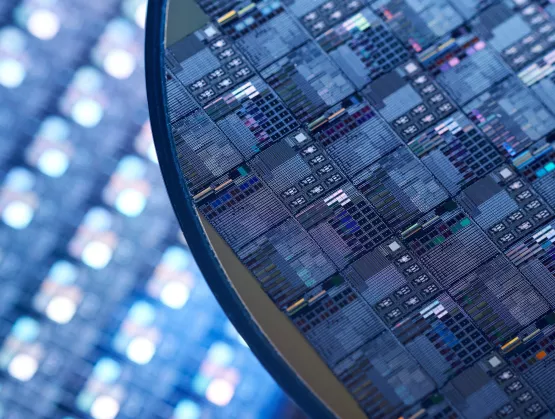
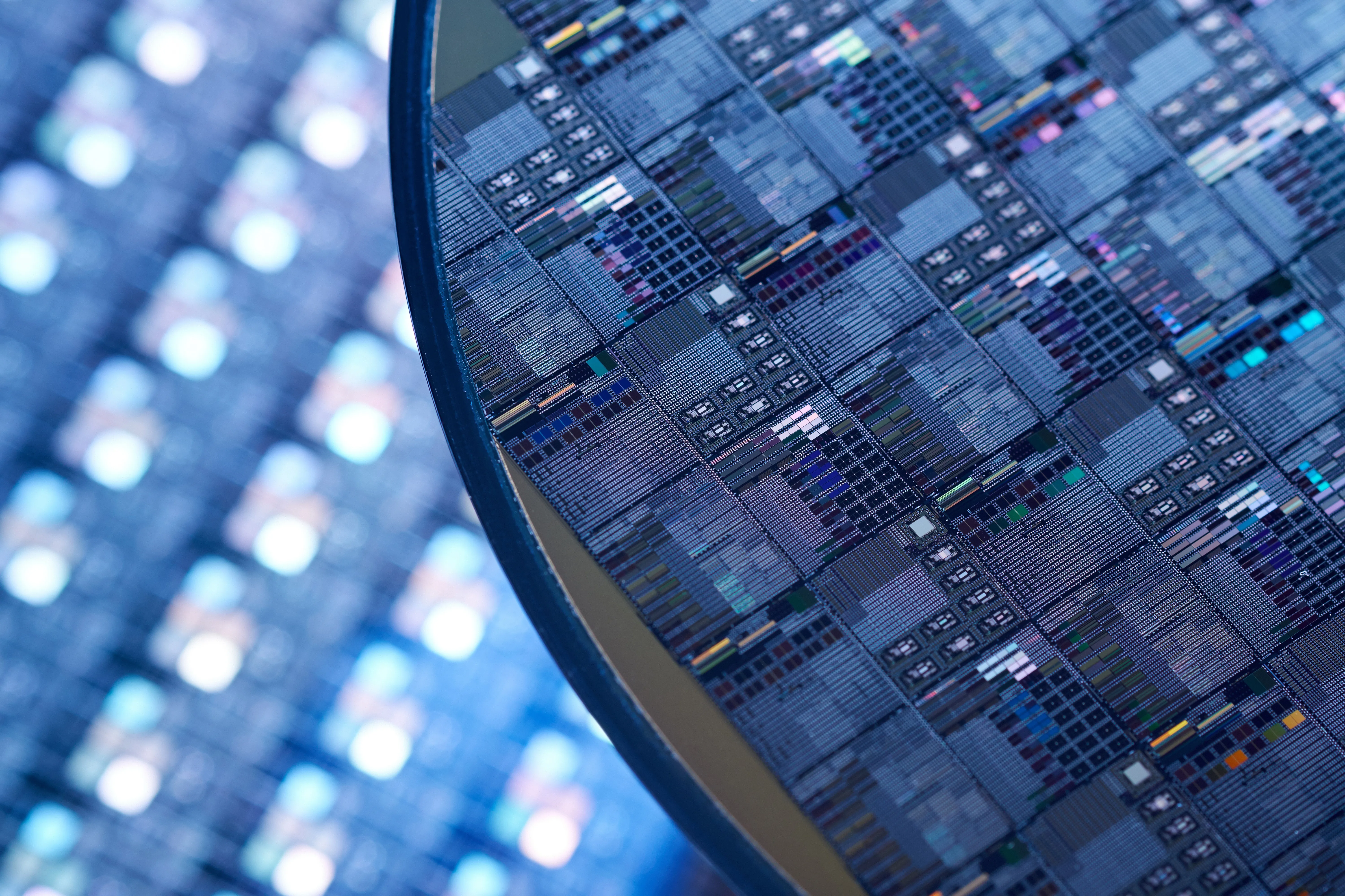
Korea is on track to top all other regions in fab investment, spending $63 billion between 2017 and 2020, with powerhouses Samsung Electronics Co. and SK Hynix leading the way, according to latest World Fab Forecast Report by SEMI. Samsung Electronics increased fab investments $770 million to $12 billion this year, and SK Hynix upped its spending a significant $2.8 billion to $7.25 billion in 2018.Korea's investment companies anticipate continued growth for both companies in the second half of 2018.Under this halo of extraordinary investment, nearly 380 SEMI Korea members and industry analysts gathered for 2018 SEMI Korea Members Day on September 13 to share insights on semiconductor market trends and new technologies that could help members bolster their competitiveness. Following are key takeaways from the event. Korea semiconductor market to grow 16% in 2018That’s according to IDC Korea VP Kim Soo-kyung, who noted that data center, memory and Internet of Things (IoT) are becoming key growth drivers for the semiconductor industry. He encouraged semiconductor companies to closely track development of automotive technology and the industry semiconductor market, both key growth areas. SEMI Korea president H.D. Cho opens SEMI Korea Members Day 2018 Continuing fab investment will lead to oversupply, but display will shineMarket entry by Chinese companies will also spur the oversupply, said Jeong Won-Seok, an analyst at HI Investment Corp. He noted that the oversupply will force Korea into stiffer competition with other regions. However, with OLED used for a wide variety of devices and the display industry seeing rapid growth, the sector will remain ripe for growth among Korean companies.Interconnecting various applications is a big semiconductor industry trendThe need for these interconnections will stand out in the mobility and high-performance computing (HPC) markets, said Park Sung-Soon, principal research fellow at Amkor Technology Korea, who addressed trends in packaging technology. He also emphasized interconnection cost efficiency as key to maximizing competitiveness.Smart Manufacturing is driving mass customizationAs semiconductor industry growth continues, production methods are shifting from ‘mass production’ to ‘mass customization,’ increasing the importance of Smart Manufacturing in driving greater production efficiency, noted BISTel VP Jeon Kyeong-Sik. Building a Smart Manufacturing platform to support large-scale production of specialized database and artificial intelligence (AI) chips will boost production efficiency, reduce costs and improve risk management. Virtual simulation will be a key enabling technology. SEMI analyst Clark Tseng presenting at SEMI Korea Members Day 2018 Surge in data volume and technology advances to drive long-term semiconductor industry growthThese key industry drivers will continue to power fab investment growth, with spending focused on 3D NAND, DRAM, and foundry, said Clark Tseng, director of Industry Research and Statistics at SEMI. China alone will see eye-watering growth with the region’s investments in domestic companies surging 46% from 2018 to 2019 and fab investment by Chinese domestic companies outpacing spending by foreign companies in China, Tseng predicted. SEMI membership rises with industry growthCulminating the event, SEMI Korea president H.D. Cho said, "With the growth of the semiconductor market, the number of SEMI members is gradually increasing, and we will help member companies grow with various activities such as Korea Members Day.”Jaegwan Shim is a marketing specialist at SEMI Korea.
Read More
Materials innovation has always been vital to the semiconductor industry. In the past, it was high-κ gate dielectrics. Today, Cobalt is seen as a replacement for Tungsten in middle-of-line (MOL) contacts.What materials innovation will the future bring?A likely answer is Graphene, the wonder material discovered in 2004.Graphene is one atomic layer of carbon, the thinnest and strongest material that has ever existed. It is 200 times stronger than steel and the lightest material known to man (1 square meter weighing around 0.77 mg). It is an excellent electrical and thermal conductor at room temperature with an electron mobility of ~ 200,000cm2.V-1.s-1. At one atomic layer, graphene is flexible and transparent. Other notable properties of Graphene are its uniform absorption of light across the visible and near infrared spectrum and its applicability towards spintronics-based devices.Graphene and Moore’s LawMoore’s Law scaling can be broken down into 4 key areas: Lithography FET Advanced Packaging (2.5D and 3D IC) Interconnect Material Solutions for upcoming nodes are starting to emerge in the first two areas (EUV and Nanowire- or Nanosheet-based FET respectively). Graphene play an important role in the latter two areas. For advanced packaging, Graphene can be used as a heat spreader (to lower overall thermal resistance), or as an EM shield (to lower crosstalk) as part of a 3D IC package.Active Graphene device layers can potentially be stacked on top of each other using a low-temperature transfer process ( 400°C) to allow for a dense heterogeneous “memory near compute” configuration. This is an area DARPA is actively researching as part of its new $1.5 billion Electronics Resurgence Initiative.Regarding interconnects, Copper interconnects are running out of steam and becoming a major IC bottleneck (projected 40% total delay for 7 nm node). Graphene’s high electron mobility and thermal conductivity make it an attractive interconnect material for MOL and back-end-of-line (BEOL), especially at line widths 30 nm.Graphene Device ApplicationsGraphene-based semiconductor applications are already starting to hit the market. A fully integrated optical transceiver (with a Graphene modulator and photodetector) operating at 25 Gb/s/channel was on display at the recent Mobile World Congress in Barcelona. San Diego-based Nanomedical Diagnostics is selling a medical device that uses a Graphene biosensor. Europe-based Emberion is building Graphene optoelectronic sensors that might find a home in LIDAR applications, where there is currently a focus on improving sensing in low-light conditions.What will the overall Graphene roadmap in the semiconductor industry look like? The history of ion implantation serves as a good example of how a fundamental scientific discovery moves from the lab to the foundry floor.The dominant view in the semiconductor industry at the time was that ion implantation would not work in practice (vs. thermal diffusion) and that, if it did, it would only marginally improve the manufacturing yields of existing products. There was nothing obvious about the transfer of ion bombardment techniques from nuclear physics research to semiconductor production.Varian (led by British physicist Peter Rose) built a new, advanced ion implant tool that Mostek (DRAM manufacturer based in Texas) was able to use to create MOS ICs with clear competitive advantages. The successful collaboration between Varian and Mostek was the turning point in the development of ion implantation as a major semiconductor manufacturing process. Over the next few years, semiconductor firms used ion implantation in a growing number of process steps and, by the late 1970s, it became one of the main processes used in semiconductor manufacturing.Likewise, the Graphene world needs to work closely with the semiconductor industry to develop the tools and techniques required to solve fundamental issues around Graphene growth (good uniformity over large area, low defect density) and Graphene transfer (high throughput, CMOS compatible). It is only then will we fully realize a future that includes 2D materials.The first step in this process is cross-industry education and initiating the dialogue between semiconductor industry and graphene companies. The National Graphene Association will be hosting the largest gathering of graphene companies and commercial stakeholders at the Global Graphene Expo Conference, October 15-17, 2018, in Austin, Texas.Learn more about graphene at the upcoming Global Graphene Expo Conference with dedicated panels of experts and investors, and roundtable discussions on how Graphene will impact the semiconductor industry. The event promo code is SEMINGA. About the AuthorAnand Chamarthy is the CEO and Co-Founder of Lab 91, an Austin-based startup that is working towards Graphene/CMOS integration at the foundry level. Anand can be reached at [email protected]. About the National Graphene AssociationThe National Graphene Association is the main organization and body in the U.S. promoting and advocating for commercialization of graphene and addressing critical issues such as standards and policy development.
Read More