downloadGroupGroupnoun_press release_995423_000000 copyGroupnoun_Feed_96767_000000Group 19noun_pictures_1817522_000000Member company iconResource item iconStore item iconGroup 19Group 19noun_Photo_2085192_000000 Copynoun_presentation_2096081_000000Group 19Group Copy 7noun_webinar_692730_000000Path
Skip to main content
Default Banner Image

Singapore

ESPOO, Finland, 22nd of March 2021 – During the past year, organizations worldwide have been forced to adapt to new ways of working and serving their customers due to the covid-19 pandemic and the related restrictions to travel and logistics. Picosun Group has significantly reinforced its local service units globally and established its PicoSupport™ Center.

PicoSupport™ Center provides on-site support and planned service items such as ALD system installations and preventive maintenance visits conducted by highly experienced, trained and certified field service engineers. It also takes care of customers’ Helpdesk and Emergency Service operations.

At the core of PicoSupport™ Center’s Helpdesk are state-of-the-art remote support tools taking advantage of augmented/mixed reality, live video, screensharing and remote connection applications. In accordance with Industry 4.0, these tools allow safe and on-time service delivery no matter the physical location or time zone of the customer. They also offer an endlessly upgradeable platform for further embedding of e.g. remote training and e-learning modules with full virtual reality environments.

Today, the remote support tools are already widely implemented in Picosun’s customer base. The remote applications are used for a number of services ranging from system inspections and troubleshooting to software upgrades, bug fixes and process optimizations.

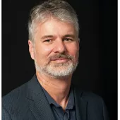
“I’m very proud to say that we have been able to adapt to the changing environment by employing new ways of interaction to ensure continued customer satisfaction. The feedback on the new remote support applications has been very positive. Customers find them easy to use and have benefitted from them in terms of faster reaction times and lower costs compared to traditional on-site services,” says Timo Malinen, VP, Service Business Area of Picosun Group.

“As our customers’ trusted strategic ALD partner we are committed to top-notch and uninterrupted services, despite of the changes in the world we operate in. We are looking forward to further enhance and develop the ways with which we can ensure smooth and trouble-free operations together with our customers,” Malinen concludes.

About Picosun
Picosun provides the most advanced AGILE ALD® (Atomic Layer Deposition) thin film coating solutions for global industries. Picosun’s ALD solutions enable technological leap into the future, with turn-key production processes and unmatched, pioneering expertise in the field – dating back to the invention of the technology itself. Today, PICOSUN® ALD equipment are in daily manufacturing use in numerous leading industries around the world. Picosun is based in Finland, with subsidiaries in Germany, USA, Singapore, Japan, South Korea, China mainland and Taiwan, offices in India and France, and a world-wide sales and support network. Visit www.picosun.com.

More information:
Timo Malinen
VP, Service Business Area, Picosun Group
Tel: +358 40 5011860
Email: [email protected]
Web: www.picosun.com

Carlsbad, CA, USA – Nordson Electronics Solutions, a global leader in electronics manufacturing technologies, are pleased to announce they will showcase many new dispensing, conformal coating, selective soldering, and surface treatment products and technologies at two events: Productronica China (Hall E6 booth #6202) and SEMICON China (Hall N4, booth #4022), both held at the Shanghai New International Expo Centre, Shanghai, China, March 17 – 20, 2021.

Nordson Electronics Solutions product lines for printed circuit board assembly are on exhibit at Productronica China, including:
• Conformal Coating - ASYMTEK Panorama™ R-Line, featuring Select Coat® SL-940 and FX-940UV Inspection system. This line provides flexibility and convenience to manufacturers who are transitioning to an automated conformal coating process.
• Fluid Dispensing – Two ASYMTEK platforms and one new valve family are featured at this show. The new Forte™ MAX System demonstrates dual-jet dispensing with two IntelliJet® jet valves including real-time skew correction - ideal for multi-up, panelized or patterned parts. The award-winning Spectrum™ II dispensing system performs tilt jetting for dispensing accurately into hard-to-reach areas. Also featured is the new Vortik® Progressive Cavity Pump for two-component fluids, which utilizes the award-winning ARC™ Technology software for ensuring easy set-up and accurate mix ratios.
• Selective Soldering - The SELECT Integra® 508.3PD 2seg multi-station includes concurrent fluxing, preheating with dual fluxers and solder pots, and can solder two singulated boards in a parallel mode in-line with two segmented conveyors.
• Plasma Surface Treatment – The popular MARCH AP-1000 is a cost- and space-efficient vacuum plasma treatment machine for treating all types of parts and components. It is completely self-contained including pump, chamber, control electronics, and requires minimal floor space.

On exhibit for semiconductor packaging at SEMICON China 2021 is the ASYMTEK Vantage dispensing system and IntelliJet® Jetting system, demonstrating dispensing for the highest levels of precision and speed.

We look forward to seeing you in Shanghai at either event!

https://www.nordson.com/en/divisions/electronics-solutions
High-resolution image: https://ndsn.tech/4cd

About Nordson Electronics Solutions
Nordson Electronics Solutions offers products to customers for precision automated fluid dispensing, conformal coating, plasma surface treatment, and selective soldering. Consisting of complementary product lines – ASYMTEK, MARCH, and SELECT – we deliver to semiconductor packaging, printed circuit board assembly, and other precision assembly operations. Our passion is helping customers take their processes further faster, with best-in-class technologies, dedicated global sales and support teams, and unmatched consultative applications expertise.

About Nordson Corporation
Nordson Corporation (NASDAQ: NDSN) is one of the world’s leading producers of precision dispensing equipment that applies adhesives, sealants, coatings and other materials to a broad range of consumer and industrial products during manufacturing operations. The company also manufactures equipment used in the testing and inspection of electronic components as well as technology-based systems for curing and surface treatment processes. Headquartered in Westlake, Ohio, Nordson has direct operations and sales support offices in more than 30 countries.

FREMONT, Calif. – Mar 15, 2021 – YES (Yield Engineering Systems, Inc.), a preferred provider of material modification and surface enhancement solutions for the semiconductor, life science and display markets, today announced that a leading memory manufacturer has ordered the YES VertaBond™ system for wafer-to-wafer and die-to-wafer bonding. The new system will be utilized in bringing next-generation HBM (high bandwidth memory) to market. It is scheduled for delivery in the second quarter of 2021 to support the customer’s R&D activities and initial production demands.

“This order marks an important milestone for YES, as it is a validation of our efforts to serve the memory market. This new VertaBond system will enable our valued customer’s most advanced HBM development and pilot production,” said Alex Chow, Asia Sales President & General Manager at YES. “We are very pleased and look forward to working with them to meet their exciting technology roadmap.”

“YES has long been a leader in cutting-edge solutions for polyimide cure and wafer-to-wafer bonding applications utilizing novel vacuum technologies. We are pleased to introduce the VertaBond system for wafers and panels, which is based on this core competence, to customers with demanding 3D stacking and heterogenous integration applications in logic, memory and other critical areas,” said Dr. Zia Karim, Sr. VP and CTO at YES.

About VertaBond
VertaBond is YES’s new vacuum-based wafer-to-wafer and die-to-wafer bonding system. Its superior temperature uniformity and low vacuum environment work together to improve the properties of bonding interfaces and eliminate voids which can cause yield loss and performance degradation. Vacuum technology enables void-free bonding in less time, reduces thermal budget, and provides excellent bonding strength and particle performance.

About YES
YES (Yield Engineering Systems, Inc.) is a leading manufacturer of high-tech, cost-effective equipment for transforming surfaces, materials and interfaces. The company’s product lines include vacuum cure ovens, chemical vapor deposition (CVD) systems, and plasma etching tools used for precise surface modification and thin-film coating of semiconductor wafers, semiconductor and MEMS devices, and biodevices. With YES, customers ranging from startups to Fortune 100 companies can create and volume-produce products in a wide range of markets, including Advanced Packaging, MEMS, Augmented Reality/Virtual Reality and Life Sciences. YES is headquartered in Fremont, California, with a growing global presence. For more information, please visit www.yieldengineering.com.

VertaBond™ and the YES logo are trademarks of YES (Yield Engineering Systems, Inc.).

SEMI Members:  $49

Use your corporate email address during log in to be recognized as a SEMI Member.

Non-Members:  $99

Students:  Free

Contact Gity Samadi ([email protected]) with a picture of your student ID to receive your discount code. 

Belgium China France Germany Ireland Italy Japan Malaysia Singapore South Korea Taiwan United States Watch Now Business Technical Featured Speakers
Highlighted content

Abstract

Fabrication in the cleanroom, and in the newer printed electronics tools, are often a function of time-varying parameters of the equipment, environment, and materials. The parameters often have co-dependencies across different process steps and tool sets. Physics based models and linear regression have been used traditionally, which are often not sufficient to learn the underlying variabilities.

This course will teach the material needed to connect cleanroom and printed electronics science and technology to that of advanced data processing capabilities enabled by Artificial Intelligence and Machine Learning. Cleanroom tools inherently can have millions of internal variables and can learn from the datasets, providing a powerful and complementary approach to traditional feedback control and process stabilization approaches.

Learning models are developed on images (CD-SEMS, optical images), time history data (Optical Emission Spectroscopy), and textual process information. A subset of the class will include: (1) Approaches to preprocess image data and create learning-based models, (2) model verification, (3) application to nanomechanical switch fabrication, and (4) cloud based implementation, data security, and data standardization.

 Course Outline:

1.      Introduction – The need for AI in microfabrication and printed electronics

a.      Microfabrication: Tool variability, process variations

b.      Printed Electronics: Inkjet variations, spatial variations

2.      Fabrication and data collection

a.      Metrology

b.      Fabrication equipment data

c.       Cleanroom data

3.      Data and image processing

a.      Types of data

b.      Time-dependent data

c.       Spatially varying data

d.      Size of data

e.      Computational capabilities

4.      AI and machine learning algorithms

a.      Regression

b.      Binary trees

c.       Random forests

d.      Deep Neural Nets (e.g. Image to Image translation using Pix2Pix)

5.      Results and outlook

a.      Improvement in linewidths

b.      Cloud based implementations


About the Instructors

Amit Lal
Amit Lal is the Robert M. Scharf 1977 Professor in the School of Electrical and Computer Engineering at Cornell University, Ithaca, NY. His work has resulted in new fabrication approaches and architectures in Micro/Nano-Electromechanical Systems, Physical Acoustics and Ultrasonics, Inertial Sensors, Biomedical MEMS, Analog Circuit Design, Solid-State Electronics, Radioactive Thin Films for Autonomous Microsystems, and Nanofabrication. The current focus of his research is on: (1) Gigahertz Ultrasonic for chip-scale communications, sensing, and computation, (2) Near zero power sensors for long-lifetime IoT, (3) Ultrasonic inertial sensors based on surface acoustic waves.

Peter C. Doerschuk
Peter C. Doerschuk is a professor in the School of Electrical and Computer Engineering and the Meinig School of Biomedical Engineering at Cornell University in Ithaca NY.  His interests in signal and image understanding have resulted in new algorithms for a variety of problems from microfabrication to single-particle cryo electron microscopy of biological particles.

Benyamin Davaji
Benyamin Davaji is a postdoctoral research associate in the School of Electrical and Computer Engineering at Cornell University. Ben works with Prof. Amit Lal at SonicMEMS Laboratory on developing solid-state acoustic wave inertial sensors, ultrasound neuromodulation microdevices, event-powered sensors, and methods to use machine learning and artificial intelligence to enhance micro and nanosystem design and manufacturing. He is the recipient of the 2019 Cornell achievement award for excellence in mentoring and the 2016 MEMS shark pub tank prize at the Hilton Head Conference. Before joining Cornell, Ben worked with Prof. Chung Hoon Lee on microthermal analysis and thermal microfluidic systems at Nanodevices Laboratory at Marquette University and received a Ph.D. in electrical engineering. During his Ph.D., he received the 2014 IEEE Larry Hause award and the 2014 College of Engineering outstanding TA award. 

Flexible Hybrid Master Classes are offered on many topics!  Visit this page for entire list and links to more detailed information on each one.

United States

Amit Lal
Dr. Amit Lal
Professor
Cornell University
Peter Doerschuk
Dr. Peter Doerschuk
Professor
Cornell University
Benyamin Davaji
Benyamin Davaji
Postdoctoral Research Associate
Cornell University
FlexTech

This course was recorded on May 27, 2021.  Registering now gives you access to listen to the recording.

10:00 am - 12:00 pm Off Add to Calendar Disabled America/Los_Angeles
Event format

Registration Details

SEMI Members:  $49

Use your corporate email address during log in to be recognized as a SEMI Member.

Non-Members:  $99

Students:  Free

Contact Gity Samadi ([email protected]) with a picture of your student ID to receive your discount code. 

Belgium China France Germany Ireland Italy Japan Malaysia Singapore South Korea Taiwan United States Watch the Master Class Now Battery Business Technical Featured Speakers

The course coverage includes:

  • Flexible power

    • Flexible batteries

    • Printed batteries

    • Thin batteries

  • Flexible batteries and sustainability

  • Flexible battery chemistry

    • Non-toxic flexible batteries

    • Materials for flexible batteries

    • Solid electrolytes for flexible batteries

  • Batteries for on-body electronics

  • Flexible battery testing

  • Flexible battery safety

  • Flexible battery specifications

  • Flexible battery power density

  • Flexible battery energy density

About the Instructor

J. Devin MacKenzie is the Washington Research Foundation Professor of Clean Energy and an Associate Professor of Materials Science and Engineering and Mechanical Engineering at UW.  Dr. MacKenzie is also the director of the Washington Clean Energy Testbeds, an open access laboratory with world-class printed electronics, flexible electronics and energy device fabrication and testing capabilities.  Dr. MacKenzie has 20 years of experience co-founding or leading startups in novel fabrication including as a co-founder and CEO of Imprint Energy commercializing printed  flexible batteries, as CTO of Add-Vision, a printed flexible OLED display company that was acquired in 2011, and as a VP at Kovio, an MIT spin out, leading printed Si RF device integration.  Devin also co-founded the world’s first printed electronics company, Plastic Logic Ltd. in the United Kingdom.  Previously Dr. MacKenzie was a researcher at AT&T Bell Laboratories. Prior to entering the start-up world, Devin was a postdoc in Physics at the University of Cambridge and earned PhD, MS, and BS degrees from the University of Florida and MIT. Dr. MacKenzie has over 220 patents and publications and has been cited over 10,000 times.

United States

J. Devin MacKenzie
J. Devin MacKenzie
Professor
University of Washington
- FlexTech

The Master Class covers the basics of battery terminology, chemistry and structures relevant to flexible electronics. The unique challenges related to the practical use and manufacturing of flexible batteries is discussed, as well as a summary of the current state of the art and emerging flexible battery technologies.  The presentation is 90 minutes with 30 minutes of Q&A and discussion from the participants who attended the live recording on April 20, 2021.

Flexible Hybrid Master Classes are offered on many topics!  Visit this page for entire list and links to more detailed information on each one.

10:00 am - 12:00 pm Off Add to Calendar Disabled America/Los_Angeles
Event format

Intermolecular, Inc. (“Intermolecular”), the trusted partner for materials innovation and a wholly-owned subsidiary of Merck KGaA, Darmstadt, Germany, today announced the relocation of the Silicon Valley Innovation Hub from Menlo Park to Intermolecular’s San Jose facilities, combining Merck KGaA, Darmstadt, Germany’s innovation efforts in the Bay area with Intermolecular’s services for materials and electronics, creating a unique space that empowers collaboration with startups.

The Silicon Valley Innovation Hub was established in 2017 in Menlo Park, CA. As part of the global Innovation Ecosystem of Merck KGaA, Darmstadt, Germany, it strives to identify and develop viable new businesses and technologies between the company’s existing business sectors or break new ground beyond them.

“The mission of the Silicon Valley Innovation Hub is to identify and explore untapped innovation- and business opportunities for Merck KGaA, Darmstadt, Germany. In this context, the intersection of life science and material science is becoming increasingly important and opens new areas of innovation. Having the Silicon Valley Innovation Hub and Intermolecular under one roof now will allow us and our cooperation partners to develop and test new materials for biological applications. We are very excited about these new opportunities,” states Thomas Herget, head of the Silicon Valley Innovation Hub.

Intermolecular has a unique toolset and expertise to quickly test and prove new advanced technologies and materials for semiconductor devices and electronic applications.

Having the Innovation Hub in the same building will further strengthen collaboration of the company’s businesses with startups and innovative companies in and around the Bay Area to rapidly grow their business from concept to high-volume manufacturing. The building boasts 30,000 square feet of cleanroom, chemical labs, offices, a collaboration area and event spaces.

Intermolecular’s customizable services are tailored to meet a startup’s unique needs, whether it is achieving a proof-of-principle, a first prototype, or a small series production. Intermolecular assigns experts in emerging technologies and offers its manufacturing facilities, which can run experiments 24/7to test and validate materials critical to product development. Intermolecular’s flexible methodologies and quality data help accelerate product design innovation, at any phase of a startup’s product development cycle.

“Intermolecular offers a seamless process flow that is specific and confidential to each startup, which is key to speeding time to innovation,” said Casper van Oosten, business field head and managing director for Intermolecular, Inc. “By providing startups the tools and expertise to validate their ideas, we can help them accelerate their path to new investment and speed their product introductions by giving them concrete data needed to move quickly from a research phase to full production. Having the experts from the Silicon Valley Innovation Hub now under one roof, we are looking forward to branch out into new areas and exploring collaboration opportunities that bring benefits to our customers/startups.”

“Semiconductor companies, particularly companies working on current generation and emerging memories, need to do a lot of experimentation to get the best combination of processes and materials,” said Tom Coughlin, president of Coughlin Associates. “Companies such as Intermolecular can provide efficient ways to gather and analyze the required data to make the next generations of memory possible.”

About the Silicon Valley Innovation Hub

Merck KGaA, Darmstadt, Germany’s Silicon Valley Innovation Hub supports scouting for the company’s existing businesses, with the additional objective to look between and beyond their scopes. This means evaluating new technological opportunities, building and maintaining local relationships and partnerships, and driving new business in fields such as cell-based meat.

About Intermolecular

Intermolecular is a trusted partner for materials innovation and the Silicon Valley science hub of Merck KGaA, Darmstadt, Germany and its Performance Materials business. Intermolecular explores, tests and develops advanced materials that are revolutionizing the next generation of electronics that make lives easier, entertaining and more productive. For more than 15 years, the team, methodologies and quality data have driven impactful outcomes, market opportunities and innovative product designs for customers.

About Merck KGaA, Darmstadt, Germany

Merck KGaA, Darmstadt, Germany, a leading science and technology company, operates across healthcare, life science and electronics. Around 58,000 employees work to make a positive difference to millions of people’s lives every day by creating more joyful and sustainable ways to live. From advancing gene editing technologies and discovering unique ways to treat the most challenging diseases to enabling the intelligence of devices – the company is everywhere. In 2020, Merck KGaA, Darmstadt, Germany, generated sales of € 17.5 billion in 66 countries.

The company holds the global rights to the name and trademark “Merck” internationally. The only exceptions are the United States and Canada, where the business sectors of Merck KGaA, Darmstadt, Germany operate as EMD Serono in healthcare, MilliporeSigma in life science, and EMD Electronics. Since its founding 1668, scientific exploration and responsible entrepreneurship have been key to the company’s technological and scientific advances. To this day, the founding family remains the majority owner of the publicly listed company.

Armstadt, Germany, March 4, 2021 – Merck KGaA, Darmstadt, Germany, a leading science and technology company, is changing the name of its Performance Materials business sector to Electronics. The new name is the visible result of the strategic realignment conducted over the past several years and a further milestone of the “Bright Future” transformation program, which began in 2018.

“The renaming of our business sector to Electronics is a logical step for us. After all, the new name underscores our strategic focus on the electronics industry. At the same time, it clearly illustrates our contribution to a world characterized by tremendous technological advances and exponential data growth,” said Kai Beckmann, Member of the Executive Board of Merck KGaA, Darmstadt, Germany, and CEO Electronics. “Under the ‘Bright Future’ umbrella, we’ve developed into a leading player within the electronics industry over the last few years. And with the new name Electronics, we’re now also making it clear, at a glance, what our business sector represents.”

As the company behind the companies advancing digital living, the Electronics business sector is involved in all major technology trends – be it 5G, Big Data, autonomous driving, artificial intelligence, or the Internet of Things. Thanks to these and other megatrends, the demand for ever smaller, faster and more energy-efficient electronics is continuously growing. For example, more and more of the components in modern chips are now approaching atomic dimensions.

“Bright Future” – A successful transformation program

The acquisitions of Intermolecular and Versum Materials in 2019 represented two very important moves within the scope of the ongoing transformation program. Thanks to the integration of Intermolecular, which offers unique processes and R&D capacities, Merck KGaA, Darmstadt, Germany, is now capable of making the latest material innovations available to its customers in the electronics industry even more rapidly. Through the acquisition of Versum Materials, the company has expanded its portfolio to include innovation-driven, ultra-high-purity process chemicals, gases and equipment for semiconductor manufacturing. The name Versum Materials, which has been in use separately until now, will be superseded by the new name of the business sector.

However, the name change will not have any effect on the existing organizational structure of the business sector, which comprises the three business units Semiconductor Solutions, Display Solutions and Surface Solutions. Electronics thus covers a particularly broad range of products and solutions, including high-tech materials and solutions for the semiconductor industry as well as liquid crystals and OLED materials for displays and effect pigments for coatings and cosmetics.

In September 2020, Merck KGaA, Darmstadt, Germany, raised its expectations for average annual organic sales growth of Electronics to 3% to 4% against the backdrop of its focus on the semiconductor industry, which is showing strong growth. The business sector currently generates around 90% of its sales in the two business units Semiconductor Solutions and Display Solutions.

SANTA ROSA, Calif., – February 17, 2021 – PNI Sensor, the world’s foremost expert in precision location, motion tracking, and fusion of sensor systems into real-world applications, today announced availability of the new TargetPoint TCM™ gyro-stabilized digital magnetic compass. TargetPoint TCM incorporates PNI’s high sensitivity Magneto-Inductive sensors with the latest high stability 3-axis MEMS accelerometer and 3-axis MEMS gyroscopes providing accurate orientation while in dynamic motion and in magnetically challenging environments. TargetPoint TCM excels in conditions that cause errors in traditional digital magnetic compasses.

TargetPoint TCM uses advanced magnetic distortion compensation and calibration scoring algorithms to counter the effects of hard and soft iron interference, providing highly accurate heading information in almost any environment and orientation.

TargetPoint TCM features and benefits include:
 Patented magnetic anomaly rejection algorithms eliminate errors due to magnetic distortion, even in magnetically harsh environments
 Gyro-stabilized compass for dynamic accuracy of sub-0.5 degrees of heading accuracy
 Multiple calibration methods, including 12-point hard- and soft-iron calibration methods, are available to ensure ease of calibration for all applications
 ITAR-free

“For military rangefinder and targeting systems developers who need accurate orientation in demanding conditions, TargetPoint TCM is a ruggedized digital magnetic compass built to handle weapons shock,” said Robin Stoecker, vice president of sales and marketing at PNI Sensor. “It’s an ideal choice for targeting applications that require reliability, consistency and accuracy.”

Pricing and Availability
For product specifications, download the TargetPoint TCM product sheet. For pricing and availability, please contact PNI Sales or your regional PNI representative.

About PNI Sensor
With over 30 years of experience, PNI is the world’s foremost expert in precision location, motion tracking, and fusion of sensor systems into real-world applications. PNI’s sensors and algorithms serve as the cornerstone of successful IoT projects and other mission-critical applications where pinpoint location, accuracy, and low power consumption are essential. Building on decades of patented sensor and algorithm development, PNI offers the industry’s highest-performance geomagnetic sensor in its class, location and motion coprocessors, high-performance modules, sensor fusion algorithms, and complete sensor systems. To learn more, please visit www.pnicorp.com.

Media Contact:
Robin Stoecker
PNI Sensor
Tel: +1 707-566-2260 |Email: [email protected]

Semiconductor equipment manufacturer ClassOne Technology has just released its proprietary new SoftSeal™ Plating Rotor, designed to enhance processing performance on the company’s Solstice® electroplating systems. The announcement was made by ClassOne’s CEO, Byron Exarcos and Senior Technology Director, John Ghekiere.

“Together with the plating reactor, the plating rotor design is key to maximizing on-wafer performance,” said Exarcos. “It’s responsible for distributing the electrical supply across the wafer, isolating electrolytes from the electrical contacts, and a great deal more. Which is why we’re constantly working to optimize rotor performance. The new SoftSeal is our latest and most advanced generation in Solstice rotors, and it’s already achieving unprecedented levels of electroplating uniformity along with reduced cost of ownership.”

“This highly-uniform performance comes from a combination of finely-tuned rotating-disk electrode physics and an optimized density of electrical contacts around the wafer,” said Ghekiere. "The ‘SoftSeal’ name comes from its high-performance FFKM elastomer seal which very effectively isolates plating chemistries from the wafer’s edge-exclusion zone. The new rotor also adapts automatically to substrate thickness, so it can accept thick or thin substrates without any adjustment. The design accommodates both flatted and multi-flat wafers, and it’s customizable to non-standard wafer sizes. Plus, the seal is more robust than on competitive rotors, meaning longer part life and no handling concerns.”

“In addition, the SoftSeal rotor’s low profile enables bubble-free entry into the plating bath,” Ghekiere noted. “And a unique design feature directs excess chemistry back into the bath at the end of the plating process. This is particularly important for conserving expensive plating baths such as gold. And, after processing, a special wafer retrieval method eliminates wafer flexing and stress by eliminating the need for extraction force at the center of the wafer.”

ClassOne stated that the new SoftSeal rotor is designed to fit all models of the company's Solstice electroplating systems and it will be standard equipment on all of the new tools going forward.

ClassOne Solstice systems are designed to provide high-performance, cost-efficient, single-wafer electroplating specifically for ≤200mm processing. The series includes the Solstice S8 and Solstice S4 for fully automated 8-chamber and 4-chamber high-speed production. It also includes the semiautomated Solstice LT, with up to three chambers that can be used both for process development and production. In addition to electroplating, the unique Plating-Plus™ capabilities of the Solstice platform enable it to handle many other important surface preparation functions, such as wafer cleaning, high-pressure metal lift-off, resist strip, UBM etch, and more. Class-leading performance and flexibility consistently make Solstice the tool of choice for ≤200mm plating across a range of product categories.

ECM Lab Solutions is a new offer from the ECM Group, dedicated to laboratories, research centers and universities. This offer combines equipment from three companies and four brands: ECM Technologies, ECM Greentech, SEMCO Technologies & Cyberstar.

With more than 90 years of experience in manufacturing industrial equipment, this ECM Group offer highlights the diverse and flexbile nature of ECM's technology and expertise by transitioning from heat treating steels and automotive applications to a wide range of research and specialty fields.

With advanced technologies for crystal growth, vacuum heat treatment and chemical vapor deposition, ECM Lab Solutions offers reliable solutions for semiconductor, solar, medical and other mechanical applications.