downloadGroupGroupnoun_press release_995423_000000 copyGroupnoun_Feed_96767_000000Group 19noun_pictures_1817522_000000Member company iconResource item iconStore item iconGroup 19Group 19noun_Photo_2085192_000000 Copynoun_presentation_2096081_000000Group 19Group Copy 7noun_webinar_692730_000000Path
Skip to main content
Default Banner Image

Singapore

• Total income for the first quarter of 2023 was EUR 4.6 million (first quarter 2022: EUR 3.6 million)
• Order book value increased by 12% compared to March 31, 2022
• Invitation to the presentation of the 2022 Annual Report on April 20, 2023 at 9.30 CEST

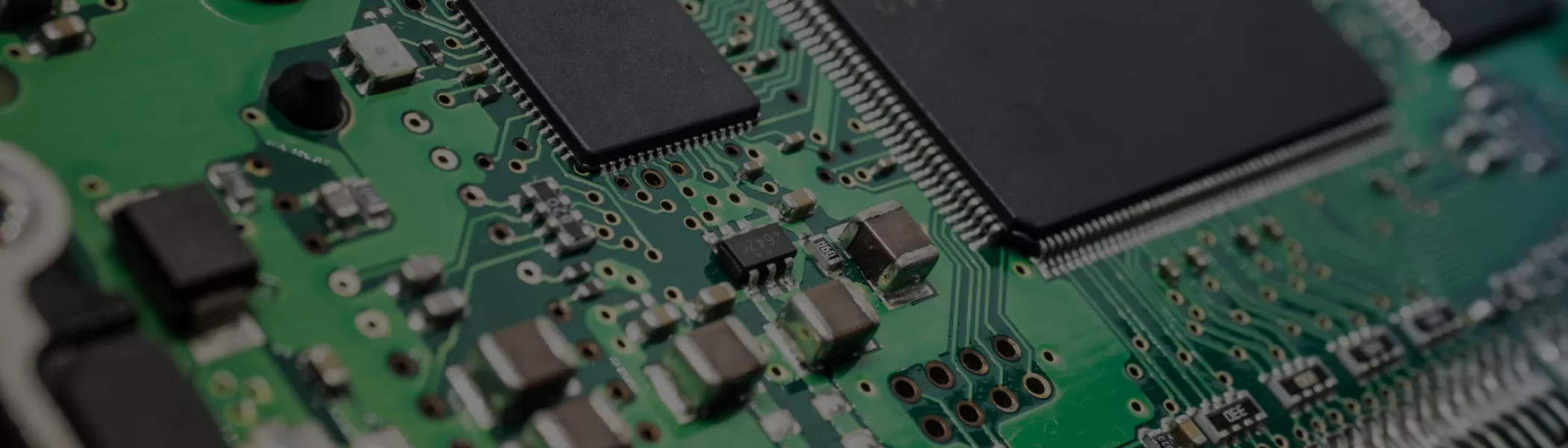
Deventer, April 13, 2023 – RoodMicrotec N.V., a leading independent company for semiconductors supply and quality services, today releases its trading update for the first quarter of 2023. The total income for the quarter was EUR 4.6 million, which is 28% higher than the total income in the first quarter of 2022. Having in mind the forecasted increase of the total income in 2023 over last year, it is encouraging to see the growth in total income in the first quarter and that the order book continues to rise. The order book contains orders for both long term contracts and engagements as well as short-term orders. The long term contracts and engagements are mainly in the SCM and Test Operations units and the short-term orders in the Failure Analysis & Qualification unit.

“I’m very proud to be able to report another increase in total income for the first quarter of 2023. We are working very hard to support our customers in their demanding test and qualification tasks and the continuous high level of total income shows that we are doing a good job”, says Martin Sallenhag, CEO of RoodMicrotec. “The steady increase in the order book is a good indicator for the rest of the year and makes us confident for the future.”

RoodMicrotec will publish the 2022 Annual Report before the opening of the Euronext Amsterdam stock exchange on Thursday, April 20, 2023. The Company’s Board of Management, Martin Sallenhag and Arvid Ladega, will comment on the report and answer questions during the conference call for media, analysts and shareholders to be held on Thursday, April 20, 2023 at 9:30 CEST.

You are invited to join the Microsoft TEAMS event using the following login instructions:
Join with your computer or mobile app Click here to join the meeting
Or call in (audio only)
+49 69 509544247 Germany, Frankfurt am Main
+31 20 399 9804 The Netherlands, Amsterdam
+32 2 895 09 68 Belgium, Bruxelles
+41 43 217 23 02 Switzerland, Zurich
Find a local number – in case you are in another country
Phone Conference ID: 124 673 558#

Outlook
RoodMicrotec expects the total income for 2023 to be in the range of EUR 17.0 million to EUR 17.5 million, with a profit before tax of 5-10% and thus in line with the financial targets. The geopolitical situation in the world and the current energy crisis throughout Europe could have an impact on the Company’s business. The Management is keeping a close eye on the situation and is doing everything possible to mitigate any potentially negative impact.

Audit
The financial data in this press release have not been audited.

About RoodMicrotec
RoodMicrotec is a leading independent company for semiconductor supply and quality services. With more than 50 years of experience in the semiconductor and electronics industry, RoodMicrotec is well-established as a highly valued partner for many companies worldwide. The Company provides full-turnkey ASIC services for complex microchips that are customized to handle specific applications for individual customers. In cooperation with strong partners, RoodMicrotec manages the entire development and production flow of ASICs in the target volume, ranging from low quantities up to multiple millions per year. The turnkey solution includes project management, wafer test, assembly, final test, qualification, failure analysis and logistics. All services comply with the industrial and quality requirements of the high reliability, aerospace, automotive, healthcare and industrial sectors. RoodMicrotec’s headquarters are located in Deventer, Netherlands, with operational units in Nördlingen and Stuttgart, Germany
For more information visit https://www.roodmicrotec.com

[April 10, 2023 – Taipei, Taiwan] Test Research, Inc. (TRI) has unveiled its latest innovation in Conformal Coating Inspection, the TR7700 SIII Ultra CI. Equipped with advanced optical design, specialized multi-phase lighting, and intelligent inspection algorithms, this cutting-edge AOI can detect coating issues with unprecedented accuracy, measure coating thickness, and inspect dispensed flux and glue.

The TR7700 SIII Ultra CI AOI can precisely measure coating thickness from critical areas on the PCB, detecting unwanted coating spills near PCB connectors, sensitive components, and designated mounting holes. The CI software can identify common coating issues, including cracks, bubbles/voids, insufficient/excess coating, and loss of adhesion, with innovative algorithms calculating the maximum/minimum coating coverage length and measuring coating length, splash, or insufficient coating. The coating thickness measurement range is from 35 μm to 750 μm.

The Smart CI AOI allows for the creation of coating maps from CAD data for rapid deployment. The smart programming also extends to learning and tuning the coating programming for an accurate inspection.

Upgrade your conformal coating inspection with TRI's latest technology. For more information about the TR7700 SIII Ultra CI, please visit the link below, https://www.tri.com.tw/en/product/product_detail-60-2-1689-1.html.

TRI's PCBA Test and Inspection solutions and Industry 4.0 data-driven management system, YMS 4.0, can help manufacturers realize their production line's full potential. These systems are designed to interoperate with other manufacturing equipment, minimize downtime, optimize production quality, and reduce operator workload.

About TRI
Test Research, Inc. (TRI) offers the most robust product portfolio in the industry for Automatic Test and Inspection solutions. From Optical Inspection to Board Testing, TRI provides the most cost-effective solutions to meet a comprehensive range of manufacturing Test and Inspection requirements. Learn more at http://www.tri.com.tw. For sales and service information, please write to us at [email protected] call +886-2-2832 8918.

PENANG, MALAYSIA - MARCH 2023 ViTrox, which aims to be the world’s most trusted technology company, is excited to announce the launch of the enhanced Tray-based Vision Handler, TR1000S⁺i!

The semiconductor business is continually changing and has grown significantly in recent decades. Some industry developments worth noticing in recent years, particularly for Integrated Circuit (IC) packages, have emerged. These trends include miniaturisation and the increased demand for IC packages due to the growth of the consumer electronics market, the automotive industry, and the medical industry.

Additionally, manufacturers are actively looking for cost-effective and well-performing equipment to secure product quality, which also includes automating inspections. Hence, we are bringing you our enhanced Tray-based Vision Handler, TR1000S⁺i! This solution is designed to cater for 360° inspection of BGA, QFP, QFN, CSP, TSSOP, MSOP, and SOP packages handled in tray-to-tape inspections.

Our TR1000S⁺i is now enhanced with an improved PP3 design with an added nozzle. The users can experience faster unit pick-and-place with three nozzles and the inspection speed is greatly improved. This translates to an average UPH increase of 24%!

The TR1000S⁺i also houses the following features:
1) Built-in de-taping module: reduces conversion time with a movable linear guide with a built-in jig.
2) Fetcher module: shortens translation time and unit pick-up time to higher throughput.
3) Auto pitching mechanism: expedites nozzle pitch conversion.
4) Easy 3D calibrations: simplifies calibration process (place and slot, no adjustments needed)‏, fast (only 5 minutes) and auto-illuminated.

In general, TR1000S⁺i is the enhanced version of the previous TR1000Si system. With the enhancement of the Tape & Reel as well as the additional nozzle piece, it will greatly reduce the Pick & Place bottleneck and generate higher throughput which compliments the high-speed vision inspection time. Thus, our TR1000S⁺i will guarantee you both quality assurance and productivity which is worth the low cost of investments. To ensure that they have a smooth automation journey with ViTrox, we have a team of technical support experts that are ready to provide top-notch services to you.

Ready to kickstart your automation journey? Reach out to us at [email protected] to learn more about how you can automate your IC package inspection effectively!

About ViTrox Technologies
ViTrox is committed to being the World’s Most Trusted Technology Company and the leading solutions provider through the most innovative, advanced, and cost-effective machine vision solution of excellent quality to its customers by integrating its technologies, people, and strategic alliances.

ViTrox offers a full spectrum of solutions, ranging from Middle & Back-end Semiconductor Inspection Solutions, SMT PCB Assembly Vision Inspection Solutions, Electronics Communication Systems, and Industry 4.0 Manufacturing Intelligence Solutions. ViTrox is headquartered in Penang, Malaysia, with offices in Asia, Germany, and the United States and sales and support sites worldwide.

For more information about ViTrox’s products and services, please visit www.vitrox.com.

SLiM 100 delivers real-time detection and quantification of VOCs to the 1 ppb level

Santa Clara, CA — March 14, 2023 — Picarro Inc., a leading provider of chemical metrology systems for advanced semiconductor fabs, today announced the SLiM 100 Lithography Process Tool Monitoring System. The new 1-ppb class chemical metrology solution detects volatile organic compounds (VOCs) in the lithography process in real time, enabling semiconductor manufacturers to quickly take steps to prevent excursions and detect non-visual defects, thereby improving yield.

As design features shrink, small amounts of airborne molecular contamination (AMC) from VOCs are resulting in significant increases in non-visual defects on reticles and wafers. Crystal growth defects on reticles, hazing of scanner optics, and t-topping of photoresists are some of the serious problems that are caused by the presence of undesired VOCs. Ultimately, these contaminants not only damage expensive lithography tools; they result in yield loss on the wafer.

To mitigate the negative effects of VOCs in the lithography process, fab operators need real-time measurements of VOCs at very low concentration levels. This is very difficult to do in the fab environment with traditional technologies because they are slow and difficult to use.

The SLiM 100 system is a real-time measurement system that is designed to run 24/7 in the fab environment. It is a fully integrated chemical metrology system that is robust, easy to operate, and is ideal for use as a high-volume process monitoring and control system. It measures and monitors 10 organic compounds that negatively affect the lithography process with concentration sensitivity down to 1 part per billion. The system can also accommodate analyzers that measure inorganic molecules at parts-per-trillion concentration levels.

“The Picarro SLiM 100 enables fab operators to detect and resolve semiconductor manufacturing issues much faster than other solutions,” said Dr. Sanjay Yedur, Director of Product Management at Picarro. “This robust system will allow them to reduce costs by halting production of defective wafers sooner and minimize downtime of lithography tools for maintenance and repair."

About Picarro Semiconductor Solutions
Picarro’s Semiconductor business offers industry leading solutions for airborne molecular contamination (AMC) and chemical contaminant monitoring within fabs and process tools. Picarro’s Semiconductor solutions respond to contaminants in seconds, not hours, enabling semiconductor manufacturers to quickly mitigate contamination events in cleanrooms, FOUP, and lithography process equipment – improving production yield. For more information, visit semi.picarro.com.

Deventer, March 8, 2023 – RoodMicrotec N.V., a leading independent company for semiconductors supply and quality services, today announces that its wholly owned subsidiary RoodMicrotec GmbH has entered into an agreement for a full and final settlement with Prime Capital Debt SCS, SICAV-FIS – Robus Recovery Sub-Fund ("Robus") regarding the perpetual bond that RoodMicrotec GmbH issued in 2010 and which is held by Robus.

As announced on 21 February 2022, Robus had initiated legal proceedings against RoodMicrotec GmbH before the Regional Court of Frankfurt am Main. Robus claimed being entitled to an 11.7% compensation payment in relation to 2017, 2018 and H1-2021. In addition, alleging non-compliance by RoodMicrotec GmbH of the terms and conditions of the 2010 perpetual bond, Robus claimed the immediate and full repayment of the nominal amount of the perpetual bond asserting grounds for the extraordinary termination of the perpetual bond. The total amount claimed by Robus in the proceedings amounted to EUR 2,568k to be increased with 11.7% interest for the applicable period.

Following an oral hearing held on 7 March 2023, the parties have reached agreement on a full and final settlement that was reached before and confirmed by the Regional Court of Frankfurt am Main. Pursuant to the settlement, RoodMicrotec GmbH shall pay a total amount of EUR 2,194k, in four equal instalments of EUR 548k each, by 31 March, 30 June, 30 September and 31 December 2023. RoodMicrotec will be able to pay the installments from free available cash.

RoodMicrotec is pleased that the ongoing litigation procedure is now settled and the dispute is closed.

About RoodMicrotec
RoodMicrotec is a leading independent company for semiconductor supply and quality services. With more than 50 years of experience in the semiconductor and electronics industry, RoodMicrotec is well-established as a highly valued partner for many companies worldwide. The Company provides full-turnkey ASIC services for complex microchips that are customized to handle specific applications for individual customers. In cooperation with strong partners, RoodMicrotec manages the entire development and production flow of ASICs in the target volume, ranging from low quantities up to multiple millions per year. The turnkey solution includes project management, wafer test, assembly, final test, qualification, failure analysis and logistics. All services comply with the industrial and quality requirements of the high reliability, aerospace, automotive, healthcare and industrial sectors.
RoodMicrotec’s headquarter is located in Deventer, Netherlands, with operational units in Nördlingen and Stuttgart, Germany.
For more information visit https://www.roodmicrotec.com

This press release is published in English and German. In case of conflict between these versions the English version shall prevail.

PENANG, MALAYSIA - FEBRUARY 2023 Wafer inspection is always a critical stage for quality assurance for wafer foundry, integrated device manufacturing (IDM), fabless, and outsourced semiconductor assembly & test (OSAT). Since semiconductor devices are continuously getting smaller and more complex, the requirement for wafer inspection has become more stringent to accommodate these changes. However, defects on the wafer may be overlooked and may pass through the final stages of fabrication and assembly if they are not eliminated or filtered out, which could be a costly mistake for the manufacturers. Consequently, this will lead to increasing demand for quality wafer production.

At ViTrox, we aim to be the World’s Most Trusted Technology Company in providing innovative, advanced, and cost-effective automated Machine Vision Inspection Solutions. Therefore, we would like to introduce our all-new Wi8i G2 PRO Wafer Vision Inspection Handler, which is designed to offer high flexibility in wafer handling, cover different semiconductor processes and high-accuracy inspection results to the users of the semiconductor market, and is also an expansion to the inspection capabilities of our existing Wafer Vision Inspection Hander - Wi8i G2.

One Solution For Two Semiconductor Processes
The all-new Wi8i G2 PRO solution is enhanced with hardware and programming features to accommodate both bare wafers (pre-dicing process) and mounted wafers (post-dicing process) inspection requirements. This innovative configuration eliminates the need for hardware conversion on the wafer robot arm when inspecting these two wafer types of the same size, which is suitable for production involving both pre-and-post-dicing processes and/or having a high-mix-low-volume of bare and mounted wafers. Hence, our Wi8i G2 PRO is the ideal solution to deliver high overall equipment effectiveness (OEE) which guarantees excellent wafer quality without any machine stop time.

Ability To Handle Up To 12” Wafers & FOUP
Based on the current market trend, there is a demand for wafer inspection equipment to cater to larger wafers due to the increasing number of chip-related productions. To address this, our Wi8i G2 PRO offers a significant enhancement in catering to a new type of wafer carrier box, Front Opening Unified Pod (FOUP) which is particularly important to users with such production practice to accommodate 12 inches of bare wafer transferring. Nowadays, FOUPs are the preferred carrier boxes to handle raw water because FOUPs offer a sealed wafer environment that provides static protection, white-light shielding, and control of moisture and oxygen. Today’s FOUPs not only address particles, but also minimize and control volatile organic compounds (VOCs), oxygen, and relative humidity. Any of these potential contamination sources can negatively impact device yield. Alternatively, should the user need to handle framed wafers, they can opt for a metal cassette instead.

Users are also able to configure their load ports based on their production needs, which can be either:
FOUP + Metal cassette
FOUP + FOUP
Metal cassette + Metal cassette

This load port design accommodates both 8 inches and 12 inches of metal cassettes on the load ports, which translates to cost-effectiveness on different-sized wafer inspections!

Robust Wafer Inspection With Our Advanced Vision Optics
Wi8i G2 PRO is not only equipped with robust vision optics that provides high-quality image under different magnification lenses but also integrates an advanced deep-learning algorithm in defect detection and determining the defect types. When a user’s wafer has a complex circuit design and/or is required to inspect different defect types at different regions, this algorithm is the perfect solution for enhancing the accuracy of defect detection.

With the combination of cutting-edge wafer handling mechanisms and robust wafer vision inspection, our latest Wafer Inspection Solution is guaranteed to solve your production pain points! Additionally, we also seek to better understand our customers’ needs in their production line and boost their production yield and also significantly reduce their long-term costs.

Interested to know more about our Wi8i G2 PRO? Do get in touch with our Sales Expert Ms Kong Poh Mei ([email protected]). To top it off, we also invite you to visit us here at ViTrox Campus 2.0 in Penang, Malaysia for a demonstration of the solution. We look forward to serving you!

About ViTrox Technologies
ViTrox is committed to being the World’s Most Trusted Technology Company to provide the most innovative, advanced, and cost-effective machine vision solutions of excellent quality to its customers by integrating ViTrox’s technologies, people, and strategic alliances.

ViTrox offers a full spectrum of solutions, ranging from Middle & Back-end Semiconductor Inspection Solutions, SMT PCB Assembly Vision Inspection Solutions, Electronics Communication Systems, and Industry 4.0 Manufacturing Intelligence Solutions. ViTrox is headquartered in Penang, Malaysia, with offices in Asia, Germany, and the United States, as well as sales and support sites worldwide.

For more information about ViTrox’s products and services, please visit www.vitrox.com.

Malaysia Singapore Register Now! Executive Technical

Co-Organizer

InvestSelangor_Logo

Supporting Partners

Highlighted content

This course will cover:

  • Substrate and PCB fabrication processes and its key processes and materials such as ABF, BT, FR5, etc.

  • Build-up micro-via technologies with use of lasers, plasma, photo materials etc.

  • Registration and tolerances of substrate design in relation to substrate and PCB fabrication processes which includes via to pattern, pattern to resist etc, which can affect microelectronics assembly processes.

  • Materials, design and surface finishes (Cu, NiAu, ENIG , NiPdAu etc) with respect to assembly processes and parameters.

  • Substrate defects and package reliability including failure of fatigue, kirkendall voids and intermetallics.

Why should I attend?

  • Provides necessary technical knowledge for industry professionals
  • Enhance knowledge in manufacturing and R&D know-how in IC packaging
  • Case studies discussion
  • Networking Opportunity with industry peers

Who should attend?

  • Directors, managers, process engineers, R&D engineers working in the areas of microelectronics
  • Useful for sale or application engineers who supply packaging materials and tools to the industry

Malaysian International Trade & Exhibition Centre (MITEC)
No. 8 Jalan Dutamas 2
50480 Kuala Lumpur
Kuala Lumpur
Malaysia

Image of Dr Lee Teck Kheng
MEET OUR SPEAKER
Dr. Lee Teck Kheng
Director, Technology Development Centre, Institute of Technical Education Singapore,
SEMI SEA Advance Packaging Technical Committee Member

Note: Program is subject to changes.

9:00 am

Introduction to IC Packaging & Interconnects

Introduction to IC Packaging
• Functions of Packaging – Mechanical, Material, Electrical and Chemical
• Review of Packaging Trend – BGA, CSP, Fan-in & Fan-out WLP, 3D Packaging, SoC vs SiP etc
• Challenges in Assembly and Packaging

Interconnects
• Overview
• TAB Bonding
• Wirebonding – Ultrasonic, Thermocompression, Thermosonic mechanisms
• Flip Chip Bondings – Thermocompression, C4, Re-cap reflow, solid-state, ACF, Conductive paste bonding

12:00 pm

Lunch

1:00 pm

Board Assembly and Soldering & PCB and IC Carriers

Board Assembly and Soldering
• Through Hole & SMT – Stencil Print Process, Reflow Profile
• Solder Materials – Alloy, Flux, Solvents, self-alignment effect
• Pb Free Solder – Ternary phase diagram, SnAgCu
• Intermetallics and Growth – Diffusion mechanism, Arrhenius equation
• Testing and Reliability – Ball shear & pull failure strength and modes, Fatigue, Weibull distribution

PCB and IC Carriers
• PCB Technology – Material properties, PCB fabrication process, drilling, patterning, plating, solder resist, laminating
• IC Carriers – Design rule, Leadframe, LTCC, Flex and BT substrates
• Substrate Development

4:00 pm

Q&A | Case Studies

5:00 pm

End of Day 1

5:00 pm

End of Day 1

9:00 am

Assembly Process

• Thickness Reduction – Grinding, Lapping, Polishing, CMP
• Dicing/Singulation – Blade, Laser, Stealth dicing, Dicing after grind
• Die Attach – Eutectic bonding, DA materials, Collets
• Plasma – Argon, Oxygen plasma, Surface tension
• Encapsulation – Mold constitutes and properties, Transfer, Film and compression molding, Dam and fill
• Plating – Solder plating, NiPd finish, PPF
• Trim & Form – ESD, Lead formation, Spring back mechanism

12:00 pm

Lunch

1:00 pm

Material Characterization Techniques

• Introduction
• Bulk Material Characterization – Stress strain, Bending, Impact toughness, TGA, DSC, TMA, DMA
• Interfaces Characterization – Failure mode and strength, Wire pull, Ball pull, Double cantilever bending, Die shear, Mold button shear, Ball shear

2:30 pm

Q&A | Case Studies

3:30 pm

Lucky Draw

3:35 pm

End of Workshop

- Workforce Development

Interaction of Substrate and PCB to Microelectronics Packaging Assembly and Reliability

Substrate and PCB technologies are the building blocks for Microelectronics Packaging and surface mount packages.

Course Fee:

Member Rate: SGD 750
Non-member Rate: SGD 935

Register before 6 March 2023 to enjoy Early Bird rate of up to 15% off the rates above.

This workshop is HRDC Claimable, subjecting to terms and conditions.

Certificate of completion will be awarded at the end of the workshop.


Off Add to Calendar 2023-03-08 00:00:00 2023-03-09 00:00:00 [IN-PERSON] Advanced Packaging Training Seminar 2023 Interaction of Substrate and PCB to Microelectronics Packaging Assembly and Reliability Substrate and PCB technologies are the building blocks for Microelectronics Packaging and surface mount packages. Course Fee: Member Rate: SGD 750 Non-member Rate: SGD 935 Register before 6 March 2023 to enjoy Early Bird rate of up to 15% off the rates above. This workshop is HRDC Claimable, subjecting to terms and conditions. Certificate of completion will be awarded at the end of the workshop.   Malaysian International Trade & Exhibition Centre (MITEC) No. 8 Jalan Dutamas 2 50480 Kuala Lumpur Kuala Lumpur Malaysia SEMI.org [email protected] Asia/Singapore public Asia/Singapore

CUPERTINO, Calif., Feb. 01, 2023 (GLOBE NEWSWIRE) -- Xpeedic today released Notus, an electronic design automation (EDA) platform for package/board SI/PI/thermal analysis, at DesignCon 2023 at the Santa Clara Convention Center in Santa Clara, Calif.

Notus, powered by Xpeedic’s electromagnetic and multiphysics solver engine, helps designers to meet the SI, PI, and thermal requirements in an efficient and automated way. It provides a comprehensive simulation flow, including DC IR-drop and AC impedance analysis, decoupling capacitor optimization, signal topology extraction, signal interconnect modeling, and thermal analysis.

In addition to Notus, Xpeedic also announced today upgrades to its Advanced Packaging and High-Speed Digital Solutions.

Metis, the EM simulation tool for 2.5D/3DIC advanced packaging designs, now delivers further improvement on performance. The unique speed-balanced-accuracy multi-mode capability is enhanced to achieve optimal accuracy-speed tradeoff.

Hermes, Xpeedic’s 3D EM simulation tool, further improves its adaptive mesh technology to achieve desired accuracy with faster convergence. It enhances the editing function associated with via, trace, and shape operation for package and PCB. It supports board-level antenna analysis and near-field and far-field view with integrated powerful data post-processing capability.

ChannelExpert, the diagram GUI-based circuit simulation platform, provides a fast, accurate and simple approach to analyze high-speed channels. It supports IBIS/AMI simulations and integrates compliance specs for various SerDes and DDR standards. ChannelExpert provides a comprehensive analysis for high-speed channels including frequency-domain S-parameter, time-domain eye diagram, statistic eye, and channel operating margin (COM) with parameter sweep and optimization. In this release, ChannelExpert integrates Hermes and Notus EM modeling tools for EM-circuit co-simulation and supports the AMI modeling and the latest DDR5 standard.

Other tools within the Xpeedic expert suite including SnpExpert, ViaEpxert, CableExpert and TmlExpert are improved with the usability and additional built-in templates to enable easy and quick evaluations of S-parameter, via, cable, and transmission line, respectively.

Availability and Pricing
Notus and the entire Xpeedic portfolio is shipping now. Pricing is available upon request.

Visit the Xpeedic website for additional information or requests for a demonstration. Email requests should be sent to [email protected].

Xpeedic at DesignCon
Xpeedic will be in DesignCon Booth #633 today and tomorrow, February 1 and February 2, at the Santa Clara Convention Center.

About Xpeedic
Xpeedic is a leading EDA provider to accelerate designs and simulations of next generation high-frequency, high-speed intelligent electronic products. Powered by its proprietary electromagnetic, circuit, and multi-physics solver technologies, Xpeedic is addressing challenges in designing IC in advanced nodes, 3D-IC with advanced packaging, high-speed digital, and RF systems for the markets including data center, automotive, communication, mobile, and IoT. Founded in 2010, Xpeedic has offices in both U.S. and China. For more information, please www.xpeedic.com.

Engage with Xpeedic
www.xpeedic.com
Twitter: @xpeedic
LinkedIn

American IC manufacturers have 56% of their wafer capacity installed at fabs located in other regions of the world, according to the new Global Wafer Capacity 2023 report from Knometa Research. As of year-end 2022, American companies have installed capacity of 4.6 million 200mm-equivalent wafers per month, with 2.0 million in domestic fabs and 2.6 million in fabs at foreign sites.

Of the major IC producing countries and regions (Americas, China, Europe, Japan, Korea, and Taiwan), the Americas region is unique in that foreign capacity exceeds that of domestic capacity.

The biggest volumes of offshore capacity for American companies are in Singapore (22% share of total), Taiwan (12%), Japan (10%), Germany (4%), Ireland (3%), and Israel (2%).

  • Singapore: Micron Technology - 4 fabs, GlobalFoundries - 4 fabs
  • Taiwan: Micron Technology - 4 fabs, Diodes - 1 fab
  • Japan: Micron Technology - 4 fabs, TI - 2 fabs, Onsemi - 1 fab
  • Germany: GlobalFoundries - 2 fabs, TI - 1 fab
  • Ireland: Intel - 1 fab, Analog Devices - 1 fab
  • Israel: Intel - 2 fabs

With its many large fabs in Singapore, Taiwan, and Japan, Micron owns by far the most offshore capacity, accounting for 65% of the 2.6 million wafers in monthly capacity. GlobalFoundries is next with a 14% share followed by Intel with 9% and Texas Instruments with 5%.

In the past couple years, American companies have announced several major fab construction projects in the U.S. Some of these came about as a result of the CHIPS Act passed by the U.S. government in July 2022 to boost American semiconductor research, development, and manufacturing.

American-owned fabs under construction in the U.S. and scheduled to open during 2024-2025 include:

  • Intel - Fabs 52 and 62 in Chandler, Arizona
  • Texas Instruments - Fabs SM1 and SM2 in Sherman, Texas
  • Intel - Fab 27 in New Albany, Ohio
  • Micron - Fab in Boise, Idaho

Micron will also build a large fab site in Clay, New York, but this project is part of the company's long-term capacity expansion plans and construction will not begin until 2024 at the earliest. In January 2023, Analog Devices announced plans to double the capacity of its fab in Beaverton, Oregon.

While the share of domestic IC wafer capacity will increase some in the next several years with the opening of these large new fabs in the U.S., American companies are building or have plans to build additional fabs at overseas sites as well. Moreover, Intel's pending acquisition of Tower Semiconductor, with its fabs in Israel and Japan (as well as the U.S.), will shift the balance in the direction of more foreign capacity. Had Tower been part of Intel at the end of 2022 with the headquarters of the combined operations being in the U.S., the foreign share of American-owned capacity would be one percentage point higher at 57%.

About Global Wafer Capacity 2023
Global Wafer Capacity provides a detailed examination of existing fab capacity along with a five-year forecast to 2027. The report has been published on an annual basis since 2007, initially by IC Insights. In December 2021, IC Insights transferred business associated with Global Wafer Capacity to co-founder Trevor Yancey. Mr. Yancey became an independent contractor in 2014 but continued as the principal analyst and project manager for Global Wafer Capacity. Published in January 2023, Global Wafer Capacity 2023 is sold by Mr. Yancey’s company Knometa Research. For more information, visit https://knometa.com/gwc.

About Knometa Research
Knometa Research is a semiconductor technology and market analysis firm led by former IC Insights executive, Trevor Yancey. Mr. Yancey co-founded IC Insights in 1997 with Bill McClean and Brian Matas. In 2014, Mr. Yancey established Knometa Research to serve as an independent contractor for TechSearch International and for IC Insights until that business closed in December 2022. For more information, visit https://knometa.com.

Substrate and PCB technologies are the building blocks for Microelectronics Packaging and surface mount packages

This course will cover:

  • Substrate and PCB fabrication processes and its key processes and materials such as ABF, BT, FR5, etc.

  • Build-up micro-via technologies with use of lasers, plasma, photo materials etc.