downloadGroupGroupnoun_press release_995423_000000 copyGroupnoun_Feed_96767_000000Group 19noun_pictures_1817522_000000Member company iconResource item iconStore item iconGroup 19Group 19noun_Photo_2085192_000000 Copynoun_presentation_2096081_000000Group 19Group Copy 7noun_webinar_692730_000000Path
Skip to main content
Default Banner Image

English

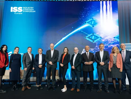
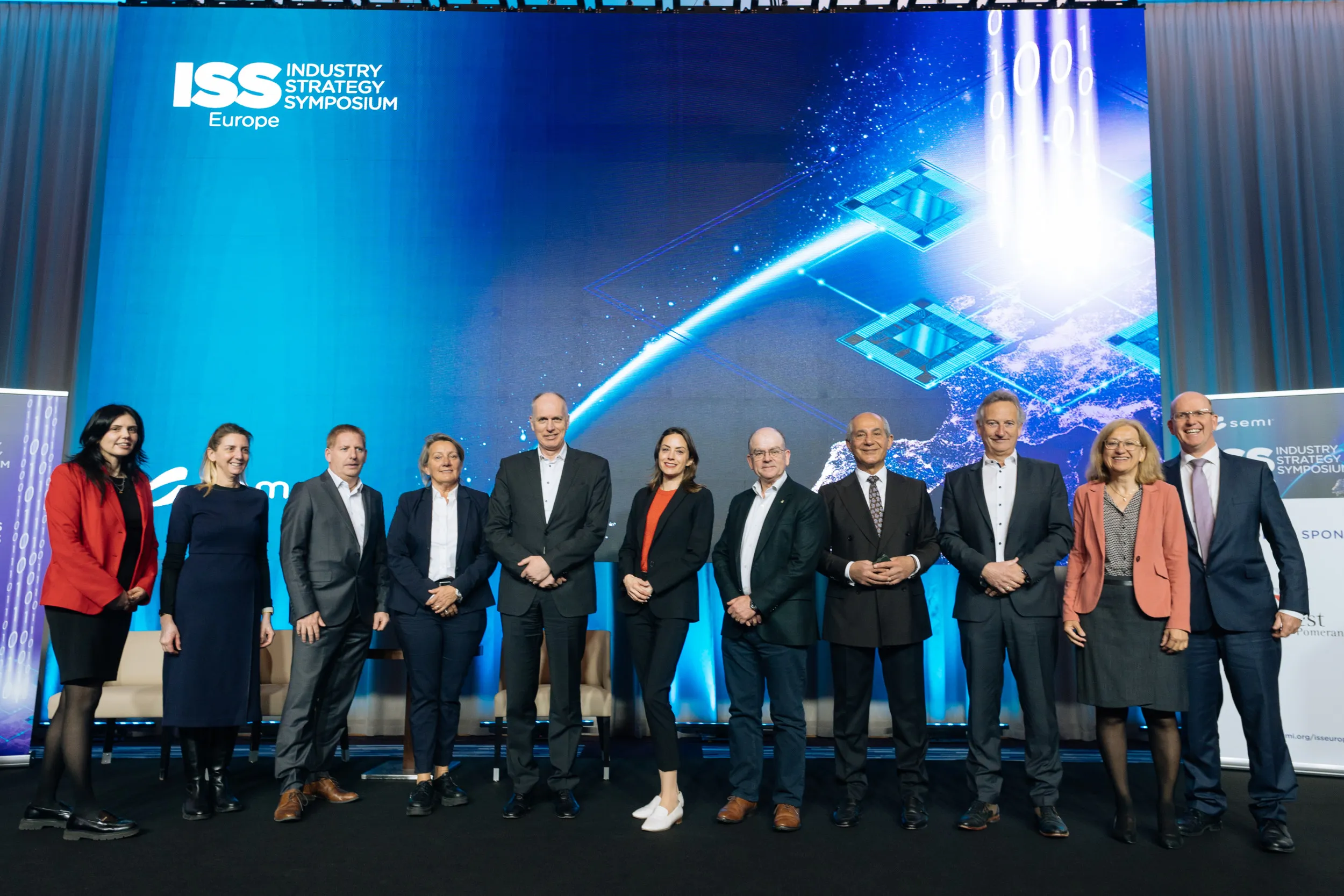
Geopolitical shifts, rapid technological advancement, and supply chain pressures continue to redefine the global semiconductor landscape. These forces framed the discussions at the 2025 SEMI Industry Strategy Symposium Europe (ISS Europe), held in Sopot, Poland. Over two days, industry leaders, and policymakers examined how Europe can boost resilience amid growing uncertainty.Artificial intelligence (AI) stood out as a key driver—powering global chip demand and transforming industry operations. In the past year, AI applications like generative models and edge computing helped push chip sales to new highs. The EU Chips Act, effective since September 2023, also fueled change. It has drawn tens of billions of euros into European semiconductor infrastructure, including major investments in Pomerania, the host region for this year’s symposium. “With AI expected to drive exponential growth in the semiconductor industry—projected to reach $1 trillion by 2030—Europe must act collectively to remain competitive,” said Laith Altimime, President of SEMI Europe. “We encourage collaboration across all countries to strengthen supply chain resilience, mitigate geopolitical risks, and harness the full potential of our diverse talent base.”Laith Altimime, President, SEMI EuropeSo what has the EU’s investment in the semiconductor industry achieved, and how much more remains to be done? Gustav Kalbe, Acting Director of Enabling and Emerging Technologies at the European Commission, cited €80 billion in public and private investment in European fabs as clear progress toward introducing "advanced technology that has not before been deployed on the continent of Europe." However, Kalbe emphasized a new urgency driven by AI’s rise. “We need in Europe a secure supply chain for AI chips in key sectors—particularly automotive,” said Kalbe. “That’s why we are really pushing for accelerated development of AI chips here.”Gustav Kalbe, Acting Director of Enabling and emerging technologies,DG CNECT, European CommissionPoland is a prime example of the EU Chips Act’s impact—driven by consistent government support. Dariusz Standerski, Secretary of State in the Ministry of Digital Affairs, highlighted Poland’s seven-pillar national semiconductor strategy, which includes expanding infrastructure and increasing engineering talent by 20% by 2030. “We need to build our production capacity to meet the strategic needs of Poland,” said Standerski. “Semiconductors are important not only because of market size, but because of their role in national security.”Dariusz Standerski, Secretary of State, Ministry of Digital Affairs, PolandRisks to the Industry from a World in Political TurmoilGeopolitical shifts and market volatility dominated the opening session of ISS Europe 2025. Malcolm Penn, CEO of Future Horizons, warned that despite strong 2024 revenues, industry fundamentals remain fragile. “All of the growth is in graphics processing units (GPUs) for AI and high-bandwidth memory (HBM) for AI servers—every other product sector is currently in recession,” said Penn. He forecast 12% industry growth in 2025 but cautioned against overcapacity and price pressures from China. “We are not seeing unit growth, and without unit growth, you don’t have sustainable market growth,” explained Penn. “If momentum in AI slows, the industry could face a significant retrenchment.”Malcolm Penn, CEO of Future HorizonsLooking beyond the immediate outlook for semiconductors, Hendrik Bourgeois, Vice President for European Governmental Affairs at Intel, turned the spotlight onbroader economic and security challenges facing the region. Bourgeois outlined four strategic policy priorities for Europe: Build internal strength to ensure external (global) relevance;Deepen alliances beyond the United States—such as with the UK, Canada, Japan, and South Korea;Be open to a stronger economic relationship with China;Recognize that the U.S. is more than its federal government: states, cities, people and corporations all have a role to play in bringing stability and certainty.Hendrik Bourgeois, Vice President for European Governmental Affairs, IntelBenedikt Ernst, Senior Vice President and Head of Strategy Transformation at Merck KGaA, Darmstadt, Germany, emphasized the strategic importance of strengthening Europe’s domestic semiconductor ecosystem. “No country or region can be fully self-sufficient,” said Ernst. “But Europe is particularly strong in domains like advanced materials, fabrication equipment, and semiconductor manufacturing. We have leading players in these fields – let’s bet on them.”Benedikt Ernst, Senior Vice President and Head of Strategy Transformation, Merck KGaA, Darmstadt, GermanyMikolaj Trunin, Deputy Director of the Invest in Pomerania, and its Strategic Investment Manager Radoslaw Bojarczuk, highlighted the region’s rising profile among global investors. Despite a global downturn in foreign direct investment (FDI) since 2015, the region stretching from Gdansk and Warsaw to Dresden and Magdeburg is emerging as a vibrant semiconductor hub. “The environment is becoming increasingly attractive to outside investors drawn by the region’s large talent pool, robust venture capital activity, and strong and stable economic growth,” said Trunin.Left: Mikołaj Trunin, Deputy Director, Invest in PomeraniaRight: Radosław Bojarczuk, Strategic Investment Manager, Invest in PomeraniaAdvancing on the Roadmap to Net ZeroThe symposium’s second session tackled sustainability—how to grow the industry beyond $1 trillion in revenue while cutting emissions. AI emerged as a key enabler of sustainable innovation. Bill Lussier, Managing Director of Tokyo Electron Europe, highlighted recycled aluminum which has a much lower carbon footprint, but noted that semiconductor equipment requires ultra-pure aluminum, which is not available off-the-shelf in recycled form. “The solution is to create a new circular economy for ultra-pure aluminum—a supply chain so complex that it cannot be managed without the aid of AI,” explained Lussier.Bill Lussier, Managing Director, Tokyo Electron EuropeAI is also helping decarbonize logistics, a critical yet often overlooked part of the semiconductor ecosystem. Rainer Kiefer, Executive Vice President and Global Head of Sales at Schenker AG, underscored the environmental cost of air cargo: “We need smart supply chain design to reduce the air miles of chips.” AI supports this by optimizing routing, loads, predictive maintenance, and demand forecasting. Rainer Kiefer, Executive Vice President and Global Head of Sales, Schenker AGHowever, AI brings new energy demands. Malgorzata Kasperska, Vice President of Secure Power at Schneider Electric, urged greater efficiency in AI data centers: “We need to optimize both power capacity and efficiency, and deploy high-density infrastructure, all while enhancing sustainability practices.” Malgorzata Kasperska, Vice President of Secure Power, Schneider ElectricEnergy-intensive fab operations remain a major challenge. Charles Vaillant, Chief Technology Officer at MANN+HUMMEL, noted that heating and ventilation account for up to 50% of a fab’s energy use. To improve efficiency, the company introduced a filtration system using activated carbon ceramic technology. The innovation reduces pressure drop, cutting fan energy use and delivering up to 41% energy savings in cleanroom environments.Charles Vaillant, Chief Technology Officer at MANN+HUMMELFinding the Talent to Fuel the Industry’s GrowthAttracting and developing talent remains a critical challenge for the semiconductor industry. Andreas Schleicher, Director for Education and Skills at the OECD, cited a visibility gap: “Young people don’t see these engineering and IT jobs. You cannot be what you do not see.” Meike Boekelmann, Chief Human Resources Officer at Comet, echoed the sentiment. “Face-to-face, we can get people excited about joining our industry,” said Boekelmann. “The challenge is getting them in front of us in the first place.” Andreas Schleicher, Director for Education and Skills,Organization for Economic Co-operation and Development (OECD)In a panel discussion on Bridging the Talent Gap for Sustainable Growth, moderated by SEMI Europe’s Maria Daniela Perez, speakers explored how industry and academia can better collaborate to meet evolving workforce demands. Thomas Kralinski, Saxon State Secretary of Economic Affairs, Labor, Energy and Climate, emphasized the importance of future-ready education. “Do we know which fab is going to be built in 2035, or which start-up will be founded? No—but all the people who will work there are already alive. We need education to prepare these people for this unknown future.Thomas Kralinski, Saxon State Secretary of Economic Affairs, Labor, Energy and ClimatePanel Discussion on Bridging the Talent Gap for Sustainable GrowthAI Intensifies Scale of Innovation in Semiconductor FabricationDay two of ISS Europe 2025 spotlighted AI’s transformative impact on semiconductor innovation, from materials to manufacturing and chip design. John Behnke, General Manager for Smart Manufacturing at INFICON, emphasized AI’s growing role in managing fab complexity. “You need a lot of highly knowledgeable people to run a fab today,” said Behnke. “They must analyze huge amounts of data, and balance priorities like quality, on-time delivery, cycle time, and profitability.” In the future, he explained, AI-powered optimization engines will shoulder that burden by making autonomous decisions.John Behnke, General Manager for Smart Manufacturing, INFICONJean-Christophe Eloy, CEO of Yole Group, pointed to the rapid growth of data centers as a catalyst for architectural transformation, predicting a shift from monolithic AI ASICs to chiplet-based designs. “In the future, we can expect to see much of the value in the semiconductor business transfer from the front-end chip to the advanced packaging that integrates chiplets,” said Eloy. Jean-Christophe Eloy, CEO, Yole GroupThis sentiment was echoed by Christophe Frey, Vice President of EU Engagement at Arm, who described the industry’s shift from systems-on-chip to systems-of-chips. “Chiplets represents a unique opportunity for Europe to re-enter the game of high-end chips,” said Frey. He emphasized the need for an open chiplet marketplace, an effort Arm supports, but warned, “There is a long road ahead of us,” citing the need for silicon qualification, profiling, test and debug infrastructure, software standards, and specifications for mechanical and thermal integration.Christophe Frey, Vice President of EU Engagement, ArmThat transition is already taking shape in manufacturing. Volker Herbig, Vice President of the Microsystems Business Unit at X-FAB, noted that capabilities developed for CMOS+MEMS sensor in the early 2000s are now enabling heterogeneous integration (HI) at scale. “We are now an open HI foundry,” said Herbig, adding that X-FAB is building a dedicated HI facility with support from the EU Chips Act. “This technology is propagating down from the high-performance computing (HPC) world to medical and industrial applications — It’s happening as we speak.”An Industry Changing Faster Than Ever Volker Herbig captured the industry’s rapid evolution with the “Red Queen” theory from Alice in Wonderland: “You need to run as fast as you can just to stay in the same place.”Volker Herbig, Vice-President, BU MEMS, X-FABClosing the symposium, Leonard Hobbs, Director for Government Affairs at Intel Ireland, cited Charles Darwin: “The species which can best adapt to changes in its environment is the one which survives,” Hobbs added, “Over the past two days we have learned much that can help Europe’s semiconductor industry to adapt successfully to a rapidly changed world.” Leonard Hobbs, Director for Government Affairs, Intel IrelandAt the symposium’s gala dinner, delegates celebrated leaders driving the industry forward. SEMI presented the 2024 SEMI European Award to Kurt Sievers, President and CEO of NXP Semiconductors, and honored Anna-Riikka Vuorikari-Antikainen, Chief Commercial Officer of Okmetic, with the Special Service Award.Kurt Sievers, President and CEO, NXP Semiconductors (Middle)Anna-Riikka Vuorikari-Antikainen, Chief Commercial Officer, OkmeticOn behalf of SEMI, the SEMI Europe team and ISS Europe committee would like to thank all speakers, sponsors, and attendees for making the event a great success.SEMI Contact Cassandra Melvin, Senior Director of Business Development and Operations Email: [email protected]
Read More
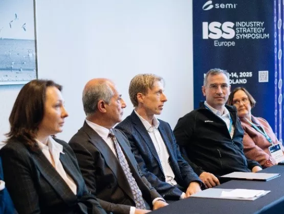
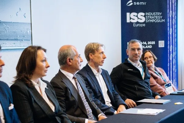
Insights from the ISS Europe 2025 Press Briefing in SopotAt the SEMI Industry Strategy Symposium Europe (ISS Europe) 2025, held in Sopot, Poland, senior leaders from government, industry, and the investment community came together to share insights on Europe’s evolving semiconductor landscape. During a dedicated press briefing, they addressed Poland’s growing role in the ecosystem, the significance of international collaboration, and the strategic levers needed to bolster Europe’s competitiveness in semiconductors.Against the backdrop of accelerating investment through the EU Chips Act, speakers emphasized that building Europe’s semiconductor future will require more than funding. It will demand cross-border collaboration, cohesive public-private strategies, and a long-term vision to ensure talent pipelines and supply chain resilience.The briefing featured remarks and commentary from:Laith Altimime, President, SEMI EuropeAgnieszka Sygitowicz, President, The Polish-Taiwanese Chamber of Commerce and IndustryPawel Pudlowski, Ph.D., Deputy CEO, Polish Investment and Trade Agency (PAIH)Monika Morali-Majkut, Chairwoman of the Supervisory Board, Atlas WardBenedikt Ernst, Senior Vice President and Head of Strategy Transformation, Merck KGaA, Darmstadt, GermanyDionys van de Ven, President, Comet YxlonAnna-Riikka Vuorikari-Antikainen, Chief Commercial Officer, Okmetic From left to right: Agnieszka Sygitowicz, President, The Polish-Taiwanese Chamber of Commerce and Industry; Pawel Pudlowski, Ph.D., Deputy CEO, Polish Investment and Trade Agency; Monika Morali-Majkut, Chairwoman of the Supervisory Board, Atlas Ward; Laith Altimime, President, SEMI Europe; Benedikt Ernst, Senior Vice President and Head of Strategy Transformation, Merck KGaA, Darmstadt, Germany; Dionys van de Ven, President, Comet Yxlon; Anna-Riikka Vuorikari-Antikainen, Chief Commercial Officer, OkmeticSEMI: How are the private sector and international partners contributing to Poland’s ecosystem development?Morali-Majkut: The private sector is essential to building Poland’s semiconductor ecosystem. At Atlas Ward, together with like-minded companies, we’ve launched SEMICON Supply Poland to help develop a strong, scalable supply chain. We’re working to ensure that essential infrastructure is ready: land, utilities, materials, and specialized service providers that can meet the needs of incoming semiconductor investments. But this isn’t just a national effort. We’re closely aligned with ecosystem-building in Dresden, Prague, and across Central Europe. Collaboration across borders is essential.Sygitowicz: We believe strongly in the philosophy of “building bridges.” In our work with Taiwan and other partners, we focus on five “bridges”: knowledge, people, business, development, and shared success. These connections are critical for Poland to become an integral part of the global semiconductor supply chain. Poland is not trying to replicate what others have done, but to learn from it—particularly in ecosystem development. The long game is not just investment attraction; it’s ecosystem maturity. SEMI: Talent shortages remain a major concern across the industry. What steps are being taken to prepare the future-ready workforce?Morali-Majkut: We are working closely with academia to build the talent pipeline Poland will need as its semiconductor sector grows. Together with industry partners, we’re developing vocational training programs and university-level collaborations aimed at aligning skills with industry needs. There are already several R D-focused projects underway at Polish technical universities, and Poland’s strong foundation in technical education positions us well to support workforce growth as the industry scales up.The semiconductor industry has one of the most complex supply chains in the world. Investing in this industry creates ripple effects across a wide range of skill areas. When we invest in semiconductor education, the spillover benefits for the broader economy will be immense.Altimime: While the talent shortage is certainly a challenge, it also presents a massive opportunity. At SEMI, we’re committed to making Europe’s semiconductor investment a long-term success. Through strong collaboration with the European Commission and a broad network of consortium partners across Europe, including Poland and other Eastern European countries, we’re pushing forward both public and private sector engagement to ensure the continuity of growth and innovation.Europe is projected to face a shortage of 271,000 skilled workers in the semiconductor sector by 2030 if current trends persist. To address this challenge, SEMI is leading a range of initiatives focused on reskilling, upskilling, and cross-sector knowledge development. We’ve established an Educational Leaders Board with 18 consortium members and are organizing events to reach out to students and educational institutions – including the recent SEMI On Campus with the University of Gdańsk — all to foster stronger connections between academia and industry. SEMI: How can Europe strengthen its semiconductor supply chain resilience in the face of geopolitical challenges?Ernst: Resilience starts with recognizing and building on Europe’s existing strengths. While much attention is often given to gaps, Europe already has world-class players, technologies, and a strong consumer market. These are key strategic assets. What’s needed now is coordination—government and industry must work together to align efforts, avoid fragmentation, and ensure that political initiatives channel support in a unified direction.Van de Ven: For industry, true resilience means the freedom to operate globally. Trade controls and IP restrictions can create bottlenecks, so policies must support open access to markets across regions—including the U.S., Europe, and Asia. Companies also need to co-create with fabs and universities, embedding themselves where talent is trained and where innovation happens. This creates a robust, future-ready ecosystem. Location decisions are increasingly influenced by proximity to both production facilities and research institutions.Sygitowicz: Poland is well-positioned to support investment through a combination of ready-to-develop land, financial incentives (such as grants and tax exemptions), and ecosystem services. Beyond infrastructure, there is growing government support for talent development and innovation. Startups, accelerators, and academic partnerships are playing a larger role in building the technology pipeline—creating a more comprehensive, innovation-friendly environment for foreign investors.Vuorikari-Antikainen: Speed is an often overlooked but critical factor in competitiveness. Europe has historically moved slowly, but if countries like Poland can create fast-track pathways for permitting, investment, and project execution, they can set themselves apart. Pairing this agility with strong education and startup ecosystems will help deliver long-term resilience and responsiveness to market needs.Altimime: We must avoid country-centric thinking. Europe’s strength lies in its diversity with different regions excel in different areas, and the challenge is to bring those strengths together. Initiatives like the pilot lines are a great example of this in action, connecting capabilities in photonics, advanced packaging, and quantum technologies across the continent. With strong leadership from Europe’s research and technology organizations (RTOs), such as the Technical Research Centre of Finland (VTT), we’re seeing renewed momentum in areas where Europe has historically been strong, like communications and photonics.To truly accelerate Europe’s position in the global semiconductor landscape, we need to focus on integration—connecting the dots between regions, institutions, and industries. From left to right: Laith Altimime, President, SEMI Europe; Benedikt Ernst, Senior Vice President and Head of Strategy Transformation, Merck KGaA, Darmstadt, Germany; Dionys van de Ven, President, Comet Yxlon; Anna-Riikka Vuorikari-Antikainen, Chief Commercial Officer, OkmeticSEMI: With the European Commission discussing a potential second Chips Act, what lessons should we carry forward from the first—and how can Poland play a stronger role?Van de Ven: The primary objective of the Chips Act should be to enable investment and industrial action. In some cases, we’ve seen frameworks become overly complex, attempting to define platforms or outcomes in ways that don’t always align with business needs. From an industry standpoint, what’s most helpful is straightforward support—mechanisms that empower companies to invest where it makes sense and move quickly. Ultimately, the private sector will determine how to build and scale the necessary infrastructure and innovation.Pudlowski: It’s true that Poland did not benefit from the first Chips Act to the extent that its assets and potential might suggest. We offer a combination of engineering talent, geographic advantage, and industrial readiness—yet, in terms of EU-level influence and visibility, we’ve been underrepresented. That is beginning to change.Poland now has a national semiconductor strategy backed by the government, and this, combined with growing engagement from organizations like SEMI, positions us for stronger inclusion going forward. At the same time, we need more bottom-up visibility. Companies in Poland should proactively present their capabilities and publish their work more widely. We have a great deal to offer, and now is the time to ensure that’s recognized in Brussels and across Europe.Altimime: Poland’s recent release of its national chip strategy is both timely and critical. From SEMI’s perspective, this is a proven model: a clear strategic roadmap, strong government backing, and industry alignment create the right environment for success. The first Chips Act delivered real progress and global attention, and with Poland’s new strategy in place, we expect to see even greater integration into the European semiconductor value chain in the next phase of the initiative.Morali-Majkut: During recent conversations with international partners, particularly in Asia, it became clear that while countries like Germany and the Czech Republic are well known within the semiconductor ecosystem, Poland has not always been equally visible—despite being geographically and industrially well-positioned. That perception is starting to shift.Poland has long played a vital role in Europe’s industrial supply chain, particularly in collaboration with Germany. We bring a strong foundation in engineering, education, cost-efficiency, and industrial land availability. These assets are highly relevant to semiconductor expansion. Rather than seeing countries in isolation, we should frame this as a collaborative regional model—linking Germany, the Czech Republic, and Poland as an integrated supply chain hub. SEMI ContactSitong He, Communications ManagerEmail: [email protected]
Read More
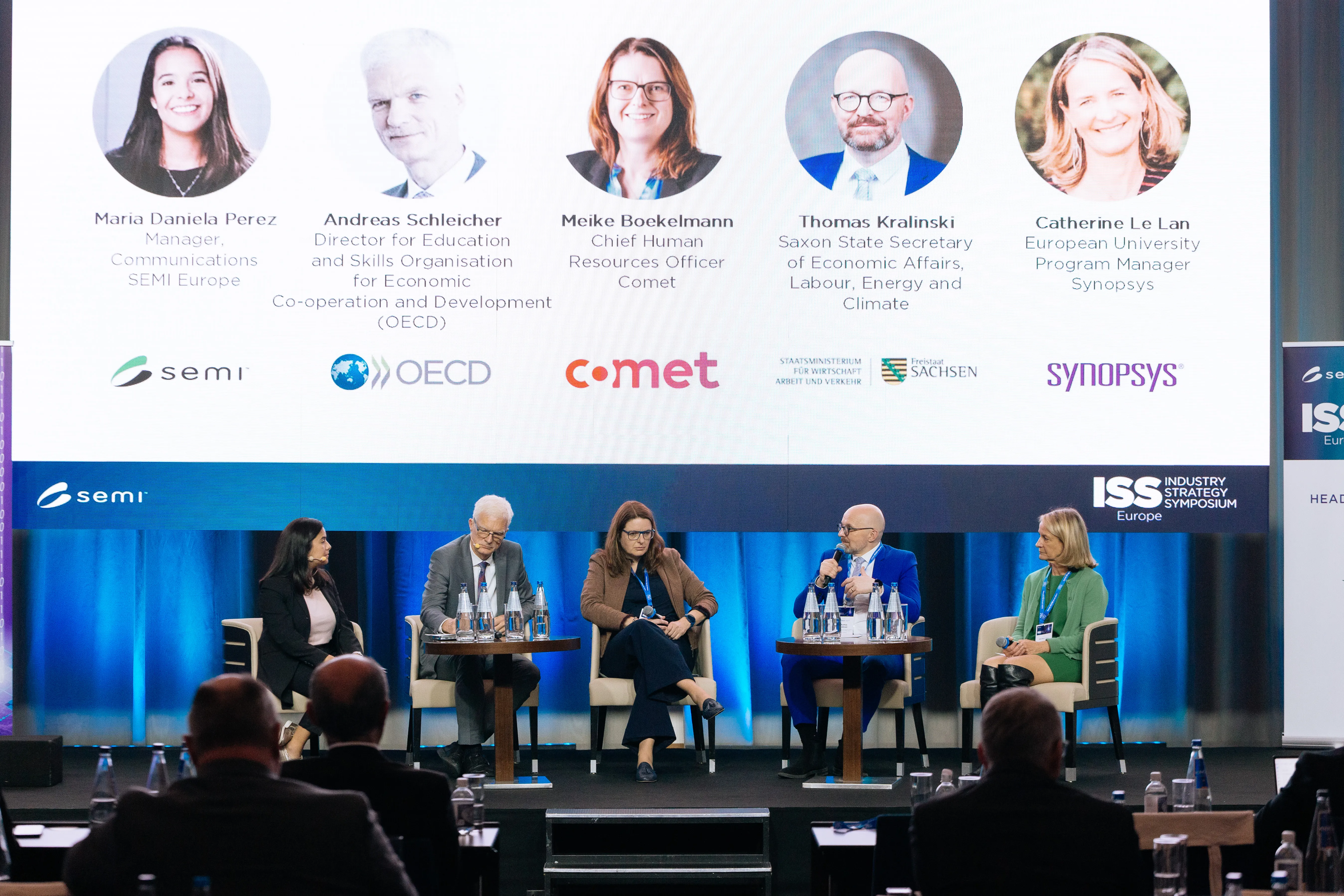
The semiconductor industry lies at the heart of Europe’s technological ambitions, powering breakthroughs in artificial intelligence, quantum computing, and advanced manufacturing. However, as the industry expands rapidly to meet surging global demand, the need for highly skilled workers is outpacing supply. According to the recently published ECSA Skills Strategy, Europe must train and hire tens of thousands of skilled professionals by 2030 to remain globally competitive. Without a robust and inclusive talent pipeline, the region’s independence in critical technologies might be at risk.At this year’s Industry Strategy Symposium Europe (ISS Europe) held in March, a panel discussion moderated by Maria Daniela Perez from SEMI Europe, brought together industry leaders and experts to explore solutions to this challenge. The discussion centered on how emerging technologies are reshaping the workforce, the role of education in preparing future professionals, and strategies for attracting and retaining diverse talent – all critical to ensuring sustainable workforce development in the semiconductor industry.Tackling Talent Acquisition and RetentionCatherine Le Lan, European University Program Manager from Synopsys, drew a direct connection between technological disruption and workforce challenges. “AI is driving unprecedented changes, and hardware is at the heart of the AI revolution,” said Le Lan. As the industry invests in new methodologies, leading-edge technologies, and innovative products, the demand for updated skillsets continues to outpace supply. This places a dual burden on companies – who must hire for both today’s and tomorrow’s skills – and on the education sector, which is expected to rapidly adapt.Meike Boekelmann, Chief of Human Resources at Comet, highlighted that the challenge is not just about attracting talent from within the semiconductor field – it is also about standing out in a crowded talent market. “We are not only competing within our industry for talent. We’re also competing against other industries: automotive, consumer electronics, and AI,” said Boekelmann. To succeed, companies must go beyond traditional incentives and offer meaningful, forward-looking career experiences. “Primarily what I see is that they’re really asking for creating an impact and also a sense of belonging… so they want to see what’s the outcome,” she explained. “There are more people leaving the labor market than entering the labor market,” added Thomas Kralinski from the Saxon State Secretary of Economic Affairs, Labour, Energy and Climate. “We need to think about immigration, family-work integration, and training.” His comments underscore the need for a holistic workforce strategy – one that not only fills immediate vacancies, but also strengthens the broader ecosystem through inclusive policies, targeted reskilling, and long-term demographic planning.Fostering Industry-Academia SynergyAs the industry evolves, so must its workforce. Andreas Schleicher, Director for Education and Skills at the OECD, made a stark observation. “There’s one thing worse than losing people – and that is to keep them and not upskill them.” He warned that the current pace of technological change demands far more than one-time training; it requires a culture of continuous learning. “Neither the industry nor the education sector has the capacity for upskilling and reskilling,” he noted, pointing out that while Europe performs well in early education, adult learning remains insufficient. “The incidence and intensity of upskilling and reskilling is so far out of what we will need.” Without scalable, lifelong learning systems, even experienced professionals risk being left behind.Building on this idea of future-readiness, Thomas Kralinski noted: “Do you know what kind of fab is going to be open in 10 years’ time or what startup is going to be founded in 10 years’ time? You probably don’t. But everybody who’s working there or will work there is born already – and is probably in school or at the university.” He underscored the need for steady investment in teachers, training systems, and educational infrastructure – not just to meet today’s demand but to ensure Europe’s long-term competitiveness.To truly inspire the next generation, Schleicher pointed to visibility as a vital factor. “You cannot be what you cannot see.” Without relatable role models or a clear understanding of how their interests connect to meaningful careers, young people – especially underrepresented students – often overlook STEM pathways. Schleicher described how even small actions, like industry professionals visiting schools to explain their work, can have a lasting impact. “You can bring someone from the semiconductors industry to speak to students and help them understand, for example, what’s in a mobile phone and that they can actually create tomorrow’s mobile phone.” That kind of engagement, he argued, helps “build dreams” and makes technology tangible, exciting, and inclusive.AI: An Enabler, Not a ThreatPanel moderator Maria Daniela Perez raised a critical question about the evolving role of AI in the workforce. Acknowledging the widespread concern that AI could lead to job displacement, she challenged the panel to consider a different perspective. How can AI be leveraged to broaden and accelerate the talent pipeline rather than replace it? In response, the panelists emphasized that AI is not a disruptor but an accelerator. Rather than eliminating jobs, AI-driven tools enhance productivity by automating repetitive tasks, freeing professionals to focus on innovation, problem-solving, and high-value work. Catherine Le Lan provided a compelling example, explaining how AI-powered electronic design automation (EDA) tools are enabling engineers to push the boundaries of technological advancement. She referred to a university study that compared two groups of students – one with access to AI tools and one without. “They found out that those AI tools helped to improve productivity and also helped to improve skills of the students,” she said. “The student who had used AI tools had better skills than the one who hadn’t used AI tools… because they had been able to focus on the high-level skills, and they got rid of the low-level skills.” Her remarks underscored how AI, when integrated into education, can accelerate both efficiency and learning outcomes.Collaboration: The Key to Sustainable Workforce DevelopmentAddressing the workforce challenge requires cross-sector collaboration among industry, academia, and policymakers. There is a shared responsibility to invest in long-term education strategies, develop structured training initiatives, and create an ecosystem where talent can thrive. This is precisely the mission of two SEMI Europe-led initiatives.The European Chips Skills Academy (ECSA) and the European Chips Diversity Alliance (ECDA) are playing a critical role in shaping Europe’s semiconductor workforce. ECSA is driving efforts to align education and training with industry needs, ensuring that both students and professionals are equipped with the technical expertise and practical experience required for the sector’s future. Meanwhile, ECDA focuses on building a more inclusive semiconductor workforce across the industry. By creating opportunities for underrepresented groups, ECDA is ensuring that the industry benefits from a broad talent pool.Securing Europe’s Semiconductor FutureIn her closing remarks, Maria Daniela Perez brought the discussion full circle, emphasizing that addressing the semiconductor talent gap requires collective ownership: “In the end, it ends up being all about collaboration,” said Perez. From engaging technology users to amplifying the industry’s visibility, to aligning with academia and policymakers, the path forward depends on shared action. By fostering this ecosystem-wide commitment – and investing in the people behind the progress – Europe can bridge the talent gap and shape a resilient, inclusive, and globally competitive semiconductor workforce.SEMI ContactKartikey Srivastava, Senior Specialist, CommunicationsEmail: [email protected]
Read More
While many individuals in leadership positions are seen as role models, only a select few have the ability to create a lasting impact on both individuals and organizations. Role models play a pivotal role in the growth of individuals, teams, and entire companies. Whether intentionally or not, role models possess the power to shape the possibilities others envision for themselves, and exceptional role models harness this power to empower and inspire.The Role Models article series shines a light on remarkable individuals who serve as inspirational leaders for their achievements, leadership, and positive influence. In each installment, we delve into the life and accomplishments of these exceptional role models, exploring their journeys, values, and the impact they've made on their organizations, communities, and across industries. Join us in celebrating these outstanding individuals and discover the valuable lessons they offer for aspiring leaders and changemakers.Role Model - Stephan HaferlIn an industry driven by innovation and high-tech advancements, Stephan Haferl stands out as a transformative leader at the helm of Comet, a globally recognized Swiss technology leader specializing in x-ray and radio frequency solutions for the semiconductor industry. As CEO, Stephan Haferl has successfully guided the company through a period of transformation, focusing on innovation, operational excellence, and customer satisfaction. With extensive experience in business management and a Ph.D. in mechanical and process engineering from the Swiss Federal Institute of Technology (ETH), Haferl has led Comet’s transformation while also contributing to the broader industry as a member of the Board of Directors at Belimed AG and the SEMI Europe Advisory Board.In this interview, Haferl shares his personal journey and leadership philosophy, offering invaluable insights into the mindset of a successful business leader and the values that drive his work. His dedication to mentorship, diversity, and cross-functional learning serves as a beacon for future generations of leaders.SEMI: Please tell us about your background and professional experience.Haferl: My father passed away from cancer when I was a young child, and though I have only faint memories of him, he left behind a remarkable legacy. He had a great library filled with books on physics, math, and engineering, as well as stories and photographs showcasing his passion for tinkering and DIY projects. In many ways, this collection became a foundation for my intellectual development. Reading his books, going through his notes from university, and exploring his projects allowed me to feel spiritually connected with him. Fortunately, his passion for the technical world was something I inherited. I became a dedicated engineer and tinkerer, and that mindset has helped me embrace every challenge I encounter. While this is a large part of “what I am”, I believe that “who I am” is even more important. That was shaped largely by my maternal grandmother. She lost her husband, my grandfather, during the war when my mother was just a baby. Despite this hardship, she remained single throughout her life, focusing on raising my mother and running my late grandfather’s little shop in post-war rural Norway. She was tougher than nails, stoic, industrious, but above all, she was humble and kind. My grandmother has been, and will always be, my role model, in both my personal and professional life. “It is my conviction and advice to aspiring leaders: If you want to be successful in business, go on a cross-functional learning journey.”– Stephan HaferlSEMI: What was your journey to becoming the CEO of Comet?Haferl: Driven by curiosity and a desire to understand as many aspects of business as possible, my journey has been one of evolution. I started in engineering and moved through various areas, including operations, R D, product management, sales, and business development. Overtime, I transitioned from being an individual contributor to a team leader, and eventually to management roles with higher levels of responsibility. There were moments when I stepped away from activities that were comfortable and familiar, like R D, in order to have new experiences and learn something new, even when it went against advice or my own judgement. I intentionally chose to become a seasoned generalist with a few areas of specialty, rather than a functional specialist. Although it may sound a bit idealistic, I never had a specific plan to end up in my current role.That said, if I could offer advice to aspiring leaders, it would be this: To succeed in business, embark on a cross-functional learning journey. Nothing prepares you more for a leadership role than hands-on experience across as many areas of business as possible.Ribbon Cutting Ceremony of the new facility in San Jose.SEMI: What has been your greatest challenge as CEO?Haferl: My greatest challenge as CEO has been and will always be, creating a healthy balance between the things I’m passionate about: the responsibilities of my job, the people around me, my family, and ultimately, myself. While a crisis or challenge in business can be overcome with the support of your entire organization and external systems, managing your time, maintaining well-being, and ensuring you’re fully present is entirely your own responsibility. The larger the role, the more demanding this balance becomes.SEMI: What has been your greatest learning as CEO?Haferl: There isn’t one single greatest learning. Instead, being a CEO offers you the opportunity to experience many truisms firsthand, such as:As a CEO, you are often alone in the spotlight and must learn to be comfortable absorbing the pressure that comes with it, entirely on your own.Your title means little unless you strive to earn it every day. If you’re a good leader, you don’t need to create followers – they will emerge naturally.A team of excellent individual contributors can be outperformed by a cohesive group – a true team of average players who stick together and go the extra miles for one another. I’ve seen this dynamic play out many times during my younger years in team sports. SEMI: What makes a great leader?Haferl: With so much literature on leadership, one might believe that there is an easy answer to this question. However, the sheer volume of attention leadership receives highlights that there isn’t a single definitive answer. I believe a great leader creates clarity and drives closure while also inspiring and motivating the team to achieve their goals while being approachable and ethical. Leadership effectiveness often depends on the team being managed, as there are various archetypal leadership styles.I’ve always aimed to build teams made up of individuals who are loyal, ambitious, disciplined, smart, honest, and kind. Within such teams, I find that a highly participative leadership style is most effective. Chinese New Year Dinner in China.SEMI: Has mentorship played a significant role in your professional success?Haferl: Mentorship has played, and continues to play, a pivotal role in my career. I have gained invaluable insights from highly experienced people who took me under their wings and showed me the ropes. Even now, as a CEO and often feeling peerless within the company, having someone to confide in and seek advice from, or get a second opinion when I am uncertain is absolutely essential.Additionally, I find it deeply rewarding to mentor two or three individuals at any given time. It is a way me to give back while continuing to learn through the process. Staying connected with younger staff is equally important – they are a valuable source of fresh insights and candid feedback.SEMI: How are you setting an example for your generation and demonstrating what you'd like to see from your generation's leaders?Haferl: Let me reframe the question by sharing the characteristics I prioritize when hiring people. As mentioned earlier, I value loyalty, ambition, discipline, intelligence, honesty, and kindness. I strive to embody these qualities in my own leadership and seek out individuals who share the same values. By consistently upholding these principles and surrounding myself with like-minded people, I aim to set a positive example and influence those around me. Townhall in Japan.SEMI: How have you helped to empower the next generation of leaders and in particular women?Haferl: I’m actively involved as mentor to a select group of high-potential employees within the company, many of whom I’ve supported for years. Even those I’ve coached who have since moved on to outside the company remain in touch, and I continue to offer guidance when needed. Interestingly, the women I have mentored have made the greatest impact, both within and beyond the company, which has been incredibly rewarding to witness. SEMI: What advice do you have for the next generation of industry leaders?Haferl: It is wise to develop a strong foundation of functional expertise in one area before expanding your knowledge. However, as a leader, you cannot rely solely on being a subject matter expert. Leadership requires understanding people, grasping the big picture, and knowing when to focus on the finer details in certain areas. To make decisive decisions, create clarity, and drive closure, you need a broad understanding of the work you’re leading. Q A with the team in South Korea.SEMI: What are the best ways to attract students and especially women to consider careers in the semiconductor industry?Haferl: Inspire them with purpose, ignite their passion, and cultivate their curiosity. Provide safe and meaningful access to the industry through internships and opportunities to work on small projects. There are many ways to pave the road for the next generation, and the semiconductor industry has the resources to make it happen. There are no excuses!SEMI: What role should diversity, equity, inclusion, and belonging play in an organization's strategy?Haferl: This is incredibly important, and I always explain to my team using this analogy: If you want to win the Champions League in football, you can’t just hire the best goalies. You need a corresponding specialist for each role to build a winning team. If you fail to treat those specialists equitably, you will lose their passion and, ultimately, their unique strength. Finally, even if you hire the best players, you’ll lose against a cohesive team of mediocre players if you don’t foster a sense of inclusion and belonging – where everyone is united as “all for one, one for all.”Groundbreaking Ceremony of Comet’s new facility in Malaysia.Through his journey and leadership philosophy, Stephan Haferl demonstrates that being a great leader is not about titles or expertise alone, but about fostering clarity and purpose, building strong teams, and nurturing those around you. His emphasis on mentorship, the importance of a diverse and inclusive environment, and the value of broadening one's knowledge to encompass all aspects of business highlights his commitment to developing well-rounded leaders. For Haferl, leadership is a dynamic balance – between personal and professional commitments, passion and discipline, and individual contributions and team success. By continuously learning, mentoring, and staying connected to the next generation of talent, he sets an inspiring example for current and future leaders in the semiconductor industry and beyond.SEMI ContactCassandra Melvin, Senior Director of Business Development and OperationsEmail: [email protected]
Read More
The European semiconductor ecosystem continues to evolve, driven by the ambitions outlined in the EU Chips Act. With goals to strengthen Europe’s technological leadership and double its semiconductor manufacturing market share to 20% by 2030, collaboration across the value chain is imperative. Heterogeneous Integration for Connectivity and Sustainability (HiCONNECTS), a Horizon Europe-funded project, exemplifies this collaborative spirit. The initiative aims to develop next-generation electronic components and systems using advanced heterogeneous integration core technology solutions.The HiCONNECTS consortium, comprising 65 partners with diverse expertise, is addressing key societal and industrial challenges. These efforts focus on advancing core technology solutions for energy-efficient, high-performance wireless and wired cloud and edge computing, as well as automotive radar systems.“Collaborating with 65 partners is no small feat—it’s akin to orchestrating a complex IT network,” says Ilan Englard, Coordinator of the HiCONNECTS project. “We streamline progress by creating local networks of partners, all interconnected through a central management framework of tasks, work packages, and coordination. Such large consortia form intricate systems where complexity fosters innovation, often leading to surprising and transformative outcomes.” As the three-year project progresses, HiCONNECTS is working to establish pilot lines focused on key areas:RF Electronic Heterogeneous IntegrationPhotonic Components for Heterogeneous IntegrationAdvanced Packaging for Heterogeneous IntegrationThese pilot lines, led by organizations such as the Ferdinand Braun Institute and imec, will develop systems and modules through advanced equipment development, manufacturing optimization, and integration of electronic and photonic components. Validation of equipment in integrated process flows will further enhance the heterogeneous integration landscape.Now in its third year, HiCONNECTS continues to welcome new members. This inclusiveness underscores the project’s flexibility and its commitment to incorporating fresh perspectives as new trends and challenges emerge. At the 12-month consortium meeting in Catania last February, Arbonaut was unanimously inducted to contribute to the forest fire use case, further expanding the project’s scope.“The upcoming months are critical, as we move closer to delivering modules, systems, and demonstrators,” says Englard. “Our goal is to heterogeneously integrate the next generation of RF, electronic, and photonic components into networking, telecom, and radar systems, with support from module and equipment makers.”HiCONNECTS members at the 12-month consortium meeting in Catania, February 2024As this ambitious work progresses, sharing project results and achievements remains a top priority for the consortium to ensure meaningful social, political, and economic impact. By drawing attention to the results of the project, the consortium enhances the visibility, comprehension, and implementation of these advancements. Recently, four partners—Excillum, TNO, SANLAB, and Centria University of Applied Sciences—participated in a webinar titled “Heterogeneous Integration for Future High Speed Communication,” organized by SEMI Europe. The webinar is now available on demand for viewers worldwide.The significance of HiCONNECTS was further highlighted at SEMICON Europa 2024, where seven consortium members presented progress on topics ranging from advanced packaging to photonic integration. At the TechARENA, representatives from SEMI Europe, Excillum, Centria, Arbonaut, AT S, imec, and Applied Materials showcased the project’s contributions to the semiconductor ecosystem. “I was thrilled to present at the TECHArena and engage with the HiConnects partners,” said Julius Hållstedt, Head of segment - Semi Electronics, Excillum. “I especially appreciated the high attendance at my talk, which validated the strong interest in X-ray solutions for semiconductor applications. The insightful discussions at the SEMICON Europa exhibition and advanced packaging conference was a rewarding bonus.”HiCONNECTS Speakers at SEMICON Europa 2024By disseminating research and breakthroughs across various channels, such as publications, webinars, and conferences, HiCONNECTS is promoting knowledge sharing and fostering collaboration across the semiconductor ecosystem. This openness accelerates the adoption of new technologies, ensuring that European industry players remain at the forefront of critical advancements. Furthermore, sharing these results strengthens Europe’s position as a hub for cutting-edge research and development, driving both economic growth and technological leadership on the global stage.SEMI Europe is proud to be a consortium member of HiCONNECTS under the Chips Joint Undertaking (Chips JU), which is funded by the EU Horizon Europe program and supported by numerous countries, including Austria, Italy, Germany, and Sweden.About HiCONNECTS:HiCONNECTS (Heterogeneous Integration for Connectivity and Sustainability) is a three-year project bringing together 65 partners to develop sustainable, energy-efficient cloud and edge computing platforms. The project focuses on high-performance computing, storage infrastructure, network interfaces, and real-time analysis of IoT sensors and big data.Kartikey Srivastava is Senior Specialist – Communications at SEMI Europe.
Read More
As artificial intelligence (AI) continues to revolutionize industries, the technology behind AI chips is advancing at an unprecedented pace. Meeting the demands of faster processing, greater efficiency, and increased complexity requires cutting-edge solutions in semiconductor manufacturing. SEMI spoke with Kai Beckmann, Member of the Executive Board at Merck KGaA, Darmstadt, Germany and CEO of the Electronics business sector, who shared insights into Merck KGaA, Darmstadt, Germany's latest strategic move that underscores the company’s commitment to innovation in semiconductor and optics technologies. With the acquisition of Unity-SC, a leading provider of advanced measurement and inspection technology, this marks a significant milestone in the evolution of AI chip manufacturing and beyond by bridging expertise in electronics and optics to drive innovation.Strengthening AI Chip Manufacturing with Unity-SC On October 31, 2024, Merck KGaA, Darmstadt, Germany’s Electronics business acquired Unity-SC, a global leader in metrology tools for semiconductors. According to Beckmann, this acquisition not only enhances Merck KGaA, Darmstadt, Germany’s portfolio in advanced measurement and quality inspection but also bolsters its position in the development of AI chips. These chips, essential for driving AI, rely on cutting-edge manufacturing processes like advanced packaging and heterogeneous integration.“Unity-SC brings precision to the table,” Beckmann explained. “Its technology is vital for managing the complex production sequences involved in creating high-density, three-dimensional chip structures. Without this precision, the production of AI chips at the necessary scale and quality would be nearly impossible.”The expertise of Unity-SC is pivotal for ensuring reliability in semiconductor manufacturing, reducing waste, and optimizing performance. With Merck KGaA, Darmstadt, Germany’s established relationships with major chip manufacturers, the integration of Unity-SC's technology is set to create synergies that will benefit the entire industry.A New Era for Merck KGaA, Darmstadt, Germany: Electronics Meets OpticsThe acquisition of Unity-SC aligns with Merck KGaA, Darmstadt, Germany’s broader strategy of combining expertise in semiconductors and optics, a vision that includes rebranding its display business as Optronics. This move represents a transformation from a traditional display specialist to a pioneer in optical technologies that complement electronic advancements. “Integrating optics with electronics opens up vast opportunities,” Beckmann shared. He highlighted key areas of focus like silicon photonics, which is revolutionizing data transmission, and augmented reality, where lightweight, powerful headsets represent the next frontier.Merck KGaA, Darmstadt, Germany’s foray into these domains underscores the importance of merging light management and materials expertise. For instance, the precision metrology brought by Unity-SC dovetails with Merck KGaA, Darmstadt, Germany’s work in materials science, forming a foundation for advancements in next-generation technologies such as quantum computing and neuromorphic systems. Driving Innovation in AIAdvanced packaging and heterogeneous integration are at the core of today’s AI revolution. These technologies make it possible to stack chips in 3D configurations, reducing energy consumption and increasing processing power. “Unity-SC plays a crucial role in this process,” Beckmann noted, emphasizing that the precise measurement of intricate structures ensures the reliability and efficiency of these complex systems.By mastering these technologies, Merck KGaA, Darmstadt, Germany is positioning itself as a leader in both materials and metrology for semiconductor manufacturing. “Integrating metrology and inspection into our portfolio is a leap forward in aligning our expertise with the needs of the AI-driven semiconductor industry,” Beckmann said. Looking AheadMerck KGaA, Darmstadt, Germany’s combination of semiconductor and optics expertise is not just about advancing technology but about creating a stronger, more resilient organization capable of tackling future challenges. The integration of Unity-SC is a step toward achieving this vision, fostering innovation at the intersection of light and materials.“Working in the semiconductor industry has always been exciting,” Beckmann shared. “But now, with AI reshaping the landscape, the opportunities for innovation and growth are unparalleled. Together with Unity-SC, we’re not just keeping pace—we’re leading the charge.”Merck KGaA, Darmstadt, Germany’s strategic evolution signals a promising future for AI, semiconductors, and the broader field of optoelectronics, where the interplay of light and materials continues to unlock new horizons.Kai Beckmann is a Member of the Executive Board of Merck KGaA, Darmstadt, Germany and CEO of the Electronics business sector. Joining Merck KGaA, Darmstadt, Germany in 1989, he has held roles in IT, consulting, and international management, including as Merck KGaA, Darmstadt, Germany’s first CIO. Since 2017, he has led the Electronics sector (operating under the name EMD Electronics in the US and Canada), driving innovation in semiconductors and optics. Beckmann also oversees the Darmstadt site and co-determination in Germany. He holds a computer science degree from TU Darmstadt and a doctorate in economics earned in 1998.SEMI ContactMaria Daniela Perez, Communications ManagerEmail: [email protected]

Read More
Use of machine learning and artificial intelligence (ML/AI) is on an exponential rise across fields1 including all aspects of the semiconductor industry. In the last decade, the use of ML/AI exploded in the areas of speech recognition, facial recognition, smart phone features, search engines and now large language models like ChatGPT, Bard AI, and CoPilot. The ML/AI growth has been enabled by massive data storage capacity and increased compute performance, leading to projections for the semiconductor industry to reach over $1 trillion in annual revenue by 2030, with about 50% of the industry’s growth related to GenAI2. Figure 1: McKinsey Company on GenAI driving semiconductor industry growthAs semiconductor manufacturing drives toward Industry 4.0, SEMI member companies have a vision of Industry 5.0, truly adaptive manufacturing, integrating human creativity with robotic precision enabled by AI. Along that path, automation and data exchange in every step of manufacturing is essential, with data acquisition, data integrity and relevance, and operational Digital Twins3 as defined steppingstones to the factory of the future.Based on growing member interest in ML/AI, in 2019, SEMI assembled technology communities that quickly engaged in AI discussions and proofs of concept, discovering gaps in the path to Industry 4.0. Successful demonstrations of the value of AI in chip manufacturing process development and factory efficiency, not to mention GenAI uses in society, hastened the pace to produce faster, more powerful chips to accommodate the computation and communication requirements. Recognizing the industry opportunity and the mounting role AI plays in the semiconductor supply chain, SEMI initiated several thought leadership efforts, namely the Smart Manufacturing Initiative, Smart Data-AI Initiative, and the Future of Computing think tank.Smart Manufacturing According to the SEMI World Fab Forecast, over 100 new and expanded wafer fabs will begin volume production by 2027. This massive capacity expansion will need to achieve the highest possible operational efficiency and performance. To this end, the Smart Manufacturing Initiative is a technology community with over 120 member companies collaborating pre-competitively to transform manufacturing. The SEMI Smart Manufacturing Global Executive Committee (GEC), outlined a roadmap vision for the cognitive factory of the future based-on technology, sustainability and future talent. The GEC has been working with members to realize that vision. Figure 2 describes this vision in terms of the technology progression needed and the approximate timeline for implementation by most manufacturers. The proliferation of this vision through Smart Manufacturing Forums at SEMICON events around the globe, newsletters and blogs has garnered enormous interest and participation in the initiative and is central to the mission of connecting and raising awareness within the ecosystem. Figure 2: AI-Driven Smart Factory (Point Systems to Autonomous Solutions) To move the needle on this vision, industry experts in the initiative successfully created and launched the Industry 4.0 Readiness Assessment Model (IRAM) to help assess technology deployment progress. IRAM adoption is steadily growing. Modern front-end and back-end lines produce an extraordinary amount of multi-modal data from a variety of sources, and this is key to success in unlocking the potential of AI in manufacturing environments. The initiative’s global working groups on Data Architectures and Smart Control Room among others are working towards a holistic Cognitive Factory framework uniting the vertical and horizontal flow of information. Integral to the Cognitive Factory are smart manufacturing standards, that will accelerate the vision outlined above, and without which local solutions are unlikely to scale.In 2023, the Smart Manufacturing Initiative brought together industry leaders in a unique Digital Twin workshop to align on the state of semiconductor development and usage. The key takeaways from this workshop are captured in a white paper that highlighted the need to accelerate efforts in multiple areas including standards. Along with SEMI International Standards, Smart Manufacturing supports other standards development organizations (SDOs) and NIST standards development, for example, to identify and drive critical standards for Cognitive Factory implementation. The initiative is planning future workshops on Cognitive Factory Framework requirements, Digital Twins, and Smart Data AI in the coming months. that highlighted the need to accelerate efforts in multiple areas including standards. Along with SEMI International Standards, Smart Manufacturing supports other standards development organizations (SDOs) and NIST standards development, for example, to identify and drive critical standards for Cognitive Factory implementation. The initiative is planning future workshops on Cognitive Factory Framework requirements, Digital Twins, and Smart Data AI in the coming months.The GEC has identified critical interrelationships in addition to the technology focus. At the intersection with sustainability, the initiative has formed a collaborative task force with the SEMI Semiconductor Climate Consortium (SCC) to develop a bottom-up technology roadmap that can be used as a blueprint for device makers to meet their proclaimed sustainability goals faster. The task force organized a technical session at SEMICON West 2024 and will be releasing a white paper in the near future. Similarly, the initiative is working with the SEMI Foundation to identify necessary future skills and to make training available through SEMI University. Smart Data AI – Applying AI to Semiconductor OperationsSEMI’s Smart Data-AI Initiative started by assembling a group of interested companies to explore the pivotal role AI could play in the industry and to address the criticality of data. All stakeholders agreed that a formidable challenge was (and still is) the integrity of that data and the security of sharing that data, which is considered IP to most. The optimal implementation of ML/AI techniques can only be gained by access to the comprehensive data set which is owned by numerous supply chain partners. Consequently, semiconductor R D, process and design have not yet realized the full benefit of Data-AI advances. In response, the initiative developed a framework to create value for members and support industry progress. Four pillars underpinning the strategy are:Educating stakeholdersBuilding communitiesExecuting proof-of-concept projectsDeveloping industry standardsTo explore the data challenges the subject matter experts highlighted, a collaborative proof-of-concept (POC) project was proposed in 2019 and accepted by the initiative's partners at Army Research Laboratories4 along with academic and industry partners. The project has completed two phases and is starting on its third phase under the expert guidance of an Industry Advisory Council (IAC) comprised of leaders in the Smart Data-AI community.The POC project, being conducted by principal investigators at Cornell University, demonstrated significant accomplishments from the first two phases, including:An AI model to predict device geometry by optimizing photolithography and plasma etching processesInitial demonstration of secure data-sharing techniques with software-hardware co-optimizationInnovative metrology ideas to train AI algorithms rapidlyStudents trained in cross-disciplinary skills to address the industry’s critical talent shortageFurthermore, the visionary objectives laid out at the initial stages of the POC proved to be synergistic with the strategic goals of the CHIPS Act5, which articulates the need for “collecting, aggregating, and sharing data sets that enable benchmarking and operational improvements, tools development, the creation of digital twins, and training AI models,” and that “the NSTC could develop a methodology for the voluntary sharing of data that protects the proprietary component and national security while enabling access to appropriate performance data.” Phase 3, to be completed by August 2025, will advance the state-of-the-art toward the following specific objectives:A framework to create and integrate Digital Twins of semiconductor R D and manufacturing process toolsAbility to explore processes and generate virtual devices swiftlyDefined interfaces to combine models for each process module or toolAccurate AI-based models for executing virtual process flows to build virtual devicesAdvanced solutions for secure data-sharing across the ecosystem – for example, federated learning where raw data is protected for each entity by building models locally, and only the outputs of the local models are used to build flow-level AI modelsFoundation for future industry standards for secure data-sharing and for interfaces in the virtual innovation environmentSEMI continues to build the collaborative community for Data-AI and strives to synergize with broader efforts such as the Digital Twin Manufacturing Institute, NSTC, and NAPMP in the U.S., and international standards development. Smart Data AI – System-level Innovation for AI – Future of ComputingThe cross-collaborative and synergistic objectives of Smart Manufacturing, the Smart Data-AI proof-of-concept work, and SEMI Standards merge to advance the state-of-the-art. The objective is to help members realize the full value of technology and innovation. In addition to improving semiconductor operations using AI, the efforts also strive to enable SEMI members to participate in, and ultimately profit from, market growth opportunities. Continued progress in AI is crucial both for the industry’s march towards $1 trillion in annual revenue, and for continuing to realize AI’s benefits to society.There are some hurdles to overcome in such a dynamic market. AI models, and the data they process, are outpacing hardware advances, posing a major roadblock for continued progress. As GenAI becomes more pervasive, the performance and power challenges continue to multiply, and require significant innovation in both hardware and software. While individual companies will develop competitive products in this domain, the entire ecosystem needs to evolve in a synergistic manner. As a global industry association, SEMI can play an important role in ensuring this. SEMI started a series of workshops and technology sessions to develop the community and identify opportunities and challenges. The first in this series was a joint workshop with McKinsey Co., held in October 2023, with a focus on innovations in “Domain-Specific Architectures.” Strategically, it brought together thought leaders from three diverse communities - start-ups, investors, and SEMI member companies across the supply chain. This was followed by an overcapacity audience at the Future of Computing session at SEMICON West 2024, where we explored AI-specific hardware with leaders in academia and industry. The Initiative’s next planned event in October 2024 is a focused workshop that is designed to be highly interactive and bring together visionaries and thought leaders from across the value chain – materials, devices, architectures, algorithms, and critical enabling technologies such as photonics, chiplets, advanced packaging, and 3D and heterogeneous integration. The overarching goal is to identify pre-competitive collaborative actions that would help the entire industry. The “Future of Computing” is the broad path to the industry’s future success. While AI systems are the current major wave on this path, future waves may be about heterogeneous integration of photonics and other components, and ultimately, quantum technologies joining the mainstream. SEMI continues to monitor these future trends, strengthen the ecosystem and enable innovation through pre-competitive collaboration, and accelerate implementation through standards.SEMI is fostering today’s collaborations while helping the industry navigate the future of electronics.Melissa Grupen-Shemansky is CTO at SEMI, Pushkar Apte is a Strategic Technology Advisor and Leader of the SEMI Smart Data-AI Initiative, and Mark da Silva is Senior Director of the SEMI Smart Manufacturing Initiative.Definitions and References:1https://arxiv.org/abs/2405.15828 Eamon Duede, William Dolan, Andre Bauer, Ian Foster, Karim Lakhani2McKinsey Company3Digital Twins for semiconductor manufacturing operations are dynamic, predictive, data-driven virtual models of a physical asset, process, or an entire factory, constantly synchronized with its real-world counterpart through real-time data streams and analytics4Research was sponsored by the Army Research Laboratory and was accomplished under Cooperative Agreement Number W911NF-19-2-0345. The views and conclusions contained in this document are those of the authors and should not be interpreted as representing the official policies, either expressed or implied, of the Army Research Laboratory or the U.S. Government. The U.S. Government is authorized to reproduce and distribute reprints for Government purposes notwithstanding any copyright notation herein.5“A Vision and Strategy for The National Semiconductor Technology Center (NSTC)” published by the CHIPS R D Office.
Read More
In recent years, SEMI has been increasing its attention to sustainability within the global semiconductor industry. With the formation of the Semiconductor Climate Consortium (SCC) within the SEMI Sustainability Initiative, member companies have joined hands to collaborate and collectively tackle the challenge of meeting the industry’s ambitious sustainability goals.The SEMI Smart Manufacturing Initiative is a global effort focused on the future of manufacturing in electronics that helps microelectronics manufacturers enable business value by facilitating awareness and problem-solving to reduce barriers and realize timely ROI for critical Industry 4.0/5.0 technology deployment.Addressing the Industry’s Sustainability Inflection Point The Initiative’s Accelerating Sustainability with Smart Manufacturing Task Force formed in the summer of 2023 is a pivotal effort that collaborates with the SEMI Sustainability Initiative. The task force provides the “how” to the “what” of corporate sustainability goals, focusing on a bottom-up approach that leverages various sensing technologies, at the cleanroom, sub-fab and facilities levels for both greenfield and brownfield device-making facilities, to enable predictive analytics.The task force is designed to be a driving force to encourage the industry’s shift from a fragmented, top-down approach – which does not address the increasing usage of carbon as device-making becomes more complex – to a more integrated, bottom-up strategy. The task force has created a roadmap based on three pillars comprising connecting, sensing, and predicting technologies, which are meant to be cumulative and could dramatically reduce the carbon footprint for making microelectronics like semiconductors. The task force participants believe this to be the first industry roadmap to address all areas of fab processing, leveraging Industry 4.0/5.0, including AI for the purpose of enhancing the sustainability of operations.The task force’s roadmap is comprehensive and includes a variety of sensing technologies, digital twin methodologies, and machine learning/AI techniques for reducing Scope 1 (direct, process-based) and Scope 2 (indirect, energy-related) greenhouse gas (GHG) emissions, water usage and material waste. Once the roadmap is completed, factory management can prioritize the implementation of best practices based on the quantified impact factors of specified use cases. The roadmap outlines methodologies for brownfield and greenfield fabs separately based on practical capex and implementation recommendations.The task force has finalized its assessment of practical solutions for reducing Scope 1 and Scope 2 emissions, and it is now addressing water usage best practices before addressing material waste later this year and into 2025. SEMI will publish separate white papers regarding Scope 1 and 2 as a precursor to offering the roadmap as a customized tool for fabs.The semiconductor manufacturing industry stands at an inflection point from a sustainability perspective. Consider this: U.S. CHIPS Act funding is set to support 19 greenfield fabs, which collectively will consume the equivalent of 11 Empire State Buildings’ worth of steel. That’s a monumental environmental impact. Additionally, the Q2 2024 SEMI World Fab Forecast is tracking approximately 104 new fabs worldwide coming online between 2023 and 2027. Each of these fabs requires significant amounts of concrete, steel, and construction equipment, all with their own GHG footprints. This all represents a challenge that the industry must grapple with head-on.Furthermore, there is the energy-intensive nature of large semiconductor fabs, the cost implications of renewable power acquisition, and the substantial water usage by medium and mega-sized fabs. The main mission of the task force is to create an industry roadmap—a practical blueprint—for device makers to invest in sustainability, following a systematic, bottom-up approach.Accelerating Sustainability with Smart Manufacturing at SEMICON West At the Smart Manufacturing Pavilion at SEMICON WEST 2024 , a special session centered around the key components of the Accelerating Sustainability with Smart Manufacturing Task Force roadmap. Task force leaders helped coordinate a unique session to showcase the roadmap findings and detailed case studies for Scope 1 and 2 emissions. The session included speakers from Deloitte, Linkan Engineering, Micron, Solvay, Spectrum Environmental Services, and ULVAC.Accelerating Sustainability with Smart Manufacturing Session at SEMICON West 2024The opening keynote by Adeline Tay of Micron covered the company’s pioneering efforts to improve sustainability in semiconductor manufacturing. Tay highlighted how to enable a net-zero transition sooner via smart manufacturing technologies including digital twins, real-time power monitoring and optimization, lower global warming potential gas usage, and emission data visibility.The next presentation by Brian Coppa (Task Force Co-Chair) of ULVAC [1] revealed the findings of the SEMI task force roadmap, which described the most critical technologies to reduce Scope 1 and 2 emissions and quantified them with respect to impact level to help fab managers prioritize budget allocation for meeting related sustainability goals at the cleanroom, sub-fab and facilities levels. Coppa provided estimates on the substantial decreases in emissions that can be achieved (see Figure 1) using the compilation of recommended technologies (i.e. predictive analytics such as AI, machine learning and predictive maintenance) that are outlined in the task force roadmap. Figure 1: Task force roadmap estimates for the emissions reduction potential for Scope 1 and 2, respectively.Jake Townsend of Deloitte [2] followed and underlined the industry’s sustainability challenge with regards to chip-making carbon footprint and the opportunities from design to fab, to sub-fab and facilities. Townsend presented that the industry’s water management carbon footprint is estimated to be at least 2 orders of magnitude higher by weight compared to consumer products such as a car or hamburger.Next, Steve Hall of Spectrum Environmental Solutions [3] discussed how compliance testing and measurements differ from common GHG reporting, which is calculation based. The Electronics Code for Federal Regulations 40CFR 98 Subpart 1 now requires the electronics industry to report both calculated emission factors and smokestack measurements. Hall showed the benefits of Fourier-transform infrared spectroscopy (FTIR) monitoring at the smokestack level and the accuracy it can provide for reporting.Michael Peter Pitroff of Solvay [4] provided an in-depth case study on how the F2-based cleaning gas Solvaclean® can replace SF6 chemistries for chamber cleans, facilitated by in-situ gas monitoring techniques, to reduce Scope 1 emissions in plasma etch and deposition processes. Pitroff covered the financial and throughput impacts of the replacement and described how higher global warming potential (GWP) gases can be replaced with low GWP gases in Bosch wafer etch processes.Finally, Drew Horseman of Linkan Engineering [5] presented innovations in water treatment for the semiconductor industry. Horseman covered current state-of-the-art, energy-efficient reverse osmosis (RO) systems and addressed specific benefits of RO optimization. He showed how data acquisition and analytics are the first step to eventually reaching zero-liquid-discharge (ZLD), which is the future of sustainable water treatment.Get Involved!Overall, the Smart Sustainability session at the Smart Manufacturing Pavilion at SEMICON West 2024 enlightened many attendees on how smart manufacturing technologies like AI can help advance sustainability in semiconductor manufacturing using a more scalable, automated approach. Visit the SEMI Smart Manufacturing Initiative homepage to learn more about upcoming activities and contact [email protected] to get involved in the task force.Amit Srivastava is Manager, Data Science- Smart Manufacturing and Artificial Intelligence at Micron Technology, Brian Coppa is Product Engineering Lead at ULVAC, and they lead the SEMI Accelerating Sustainability with Smart Manufacturing Task Force. Mark da Silva is Senior Director of the Smart Manufacturing Initiative and APHI Technology Community at SEMI. Topics: Smart Manufacturing , SEMI Smart Manufacturing Initiative , semiconductor manufacturing , Digital Twin standards , manufacturing productivity , Digital Twin framework , manufacturing efficiency , semiconductor industry , semiconductor ecosystem, sustainability , SEMICON West , decarbonization , Semiconductor Climate Consortium , greenhouse gas emissionsReferences from the Smart Sustainability Session at Smart Manufacturing Pavilion available to SEMICON West 2024 attendees: SEMI Smart Sustainability Roadmap: Blueprint for Device MakersGreen Chips are the New Blue-Chip InvestmentMeeting Net Zero Manufacturing Challenges with Real-Time Monitoring of Exhaust Laterals in Sub-FabsSolvaClean as replacement of SF6 in cleaning and etchingInnovations in Water Treatment: Exhibiting the Importance of Data in Sustainable Process Development
Read More