downloadGroupGroupnoun_press release_995423_000000 copyGroupnoun_Feed_96767_000000Group 19noun_pictures_1817522_000000Member company iconResource item iconStore item iconGroup 19Group 19noun_Photo_2085192_000000 Copynoun_presentation_2096081_000000Group 19Group Copy 7noun_webinar_692730_000000Path
Skip to main content
Default Banner Image

English

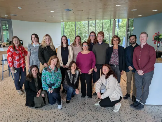
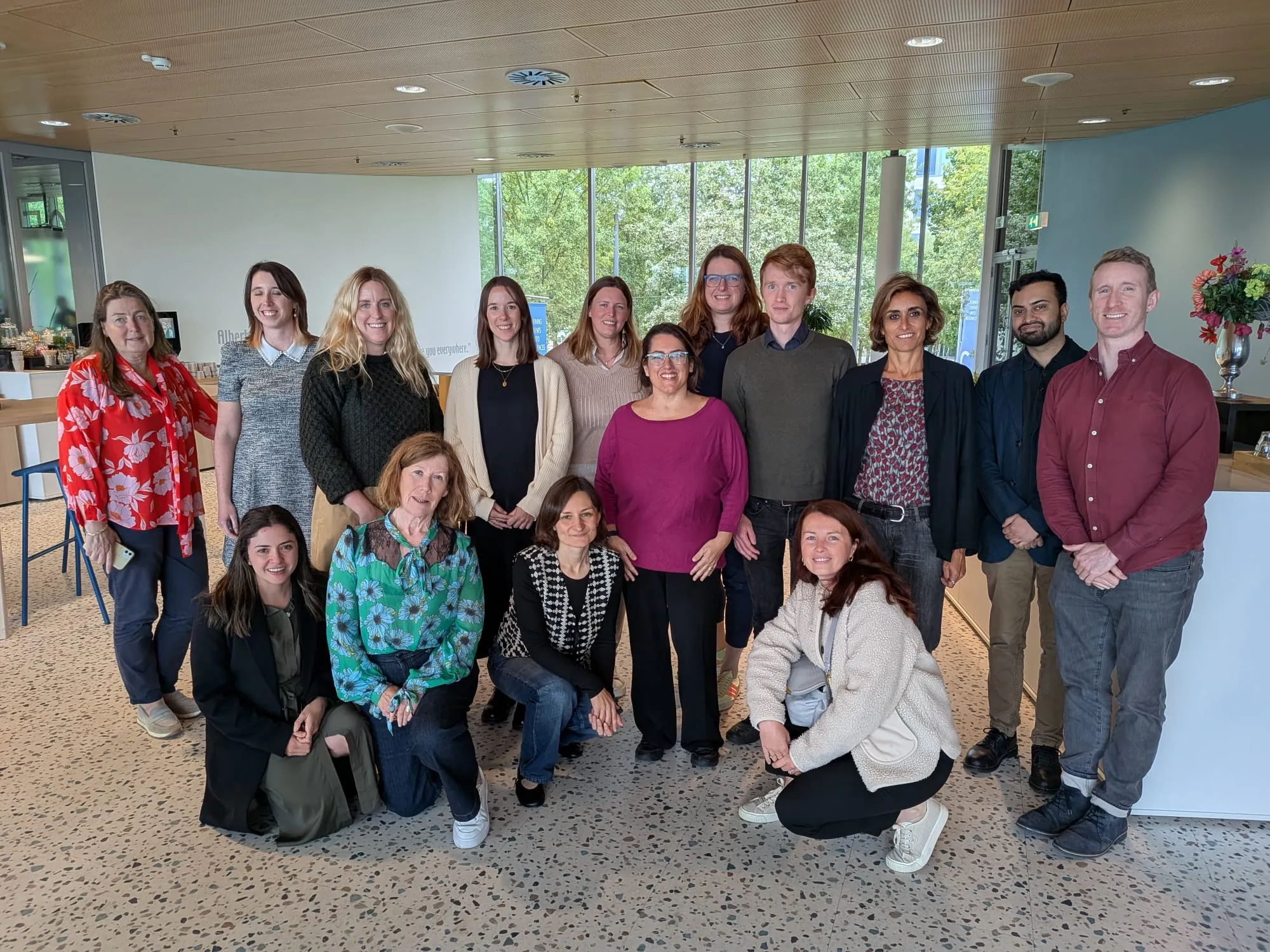
On September 16, 2025, the Inclusive Chips Forum organized by Platform Talent voor Technologie at the High Tech Campus Eindhoven convened changemakers from across Europe’s semiconductor ecosystem to share insights and strategies for building a more inclusive industry.This full-day program was designed to showcase practical strategies, inspiring case studies, and collaborative solutions aimed at strengthening inclusion, innovation, and resilience in the semiconductor industry. With Europe’s role in the global semiconductor landscape under intense focus, the forum highlighted why building a workforce culture rooted in equity and belonging is not just the right thing to do, it’s a strategic imperative.A Thought-Provoking Panel on Inclusive LeadershipA central question resonated throughout the conversation: What if inclusivity were treated as a core component of leadership development, as fundamental as financial management or strategic planning, rather than an optional module or one-off seminar?The discussion surfaced several critical insights for the industry and beyond:Awareness alone is not enough. While raising awareness about bias and stereotypes is important, research and experience show it rarely leads to behavioral change on its own. Lasting change comes from setting clear norms, leaders must define and model what is acceptable, expected, and celebrated in organizational culture. As Sahar Yadegari, Executive Director of Expertisecentrum voor haar technische ontwikkeling, emphasized:“Awareness is a starting point, not the finish line. Real change happens when inclusion is built into systems — not treated as an add-on.” – VHTOLeadership as connection. True leaders don’t just focus on profits or processes. They bring all perspectives into the room, connect diverse groups, and create conditions for others to thrive.Structural support matters. To avoid symbolic gestures, organizations must embed inclusivity into their leadership practices and accountability systems.Competitiveness through inclusion. By embracing diversity and inclusion, Europe can future-proof its semiconductor workforce, strengthening innovation capacity and securing its position in an increasingly competitive global market.Looking AheadThe Inclusive Chips Forum underscored a powerful message: embedding inclusion into leadership is not optional, it is essential for the sustainable success of Europe’s semiconductor industry.As participants engaged in lively discussions and networking throughout the day, one thing became clear: building a resilient, innovative, and inclusive semiconductor ecosystem will require collaborative effort, courageous leadership, and a commitment to turning awareness into action.A heartfelt thank you to all speakers, participants, and partners who made this event possible.For more information, contact Ana Isabel Billingslea at [email protected] or Kartikey Srivastava at [email protected] Isabel Billingslea is Communications Coordinator at SEMI Europe.
Read More
The GENESIS EU project is reshaping how Europe thinks about semiconductor manufacturing. Its goal is simple but ambitious: reduce usage of harmful chemicals from chip production, cut emissions and waste, and make the industry more circular and resilient.Launched on 1 May 2025, GENESIS – GENerate in Europe a Sustainable Industry for Semiconductor – is a research and innovation project co-funded by the European Union through Chips JU and its participating member states. In addition, Swiss partners are supported by the Swiss State Secretariat for Education, Research and Innovation (SERI).Coordinated by CEA-Leti in Grenoble, GENESIS brings together 58 partners from across the semiconductor value chain: materials and chemistry suppliers, equipment manufacturers, semiconductor fabs, research and technology organisations (RTOs), universities, small and medium-sized enterprises (SMEs), recycling specialists and communication experts. Together, they are working to build a resilient, circular and environmentally responsible microelectronics sector aligned with the European Green Deal and the European Chips Act.Mission and VisionGENESIS exists to future-proof the European semiconductor industry. The project focuses on:Eliminating or replacing per- and polyfluoroalkyl substances (PFAS) and other hazardous substances used in manufacturing processes;Reducing waste and greenhouse gas emissions throughout the production chain;Securing access to critical materials through smarter use, reuse and circular strategies;Deploying advanced monitoring and sensing solutions for gas and liquid environments in fabs.Six Work Packages, One Integrated ApproachTo reach its objectives, GENESIS is structured into six work packages.Work Package 1 – Management, Specifications, and MethodsLead: CEA-LetiWP1 keeps the project on track. It manages the technical, administrative and financial coordination of GENESIS and defines common specifications and methodologies. This includes setting technical recommendations and carrying out environmental impact assessments so that shared targets and consistent methods guide all subsequent work.Work Package 2 – Process, Monitoring Sensing Hardware and SolutionLead: CSEMWP2 develops real-time monitoring technologies capable of detecting and quantifying emissions from process gases such as NF₃, CF₄ or SF₆. By improving transparency and enabling process feedback, GENESIS contributes to the transition toward low-emission semiconductor fabs aligned with EU climate goals.Work Package 3 – Environmentally Friendly Materials AlternativesLead: imecWith global PFAS restrictions tightening, the semiconductor sector urgently needs high-performance, safe alternatives. GENESIS in WP3, is designing and qualifying materials for key manufacturing steps including lithography, etching, cleaning, deposition, and packaging, that reduce industry dependence on PFAS and higher GWP gases while ensuring compatibility with industry performance requirements.Work Package 4 – Minimisation of Waste and EmissionsLead: FraunhoferWP4 addresses the complexity of semiconductor waste streams and explores innovations to enhance abatement efficiency. GENESIS develops recycling, recovery, and closed-loop solutions for gases, slurries, and solvents, with the aim of significantly reducing waste across fabs.Work Package 5 – Materials Scarcity Impact MitigationLead: Università degli Studi di Roma Tor VergataEurope’s dependence on critical raw materials—including gallium, indium, and rare earth elements—represents both an environmental and strategic challenge. GENESIS in WP5 focuses on reducing CRM usage through process innovation and strengthening circularity to enhance supply chain resilience.Work Package 6 – Regulations, Dissemination, Communication and ExploitationLead: SEMI EuropeWP 6 is dedicated to ensuring that GENESIS creates meaningful and lasting impact beyond its technical achievements. It integrates regulatory monitoring, dissemination, communication, and exploitation activities to connect the project’s innovations with industry needs, European policy developments, and wider society. WP6 is coordinated by SEMI Europe, supported by expert partners across the consortium, and serves as the bridge between GENESIS’s scientific work and its real-world influence.Long-term strategyGENESIS is built with one goal in mind: making sure the work happening inside the project translates into real change across Europe’s semiconductor ecosystem. To support this, the project focuses on four key impact areas that help move ideas from research into industry, policy and long-term community engagement.Helping Industry Put Results to WorkA core part of GENESIS is understanding how each partner can use the project’s results in their own environment. Whether it’s new materials, smarter monitoring solutions or better waste-reduction approaches, partners define clear pathways for adoption so GENESIS innovations can move naturally into real industrial use.Staying Connected to Europe’s Policy AgendaSustainability and chemical regulations in Europe are evolving fast, and GENESIS stays close to these developments. The project brings technical insights to discussions around the Green Deal, PFAS regulation, and critical raw materials. This makes sure GENESIS is not only aligned with policy trends, but also contributes to shaping them.Making Knowledge Accessible and Future-FocusedOpen access is an essential part of GENESIS. The project shares its research outputs publicly and supports the creation of educational material for universities and training programmes. This helps the next generation of engineers and specialists build on GENESIS knowledge and carry it forward.Keeping GENESIS Visible and RelevantGENESIS maintains a strong presence across events, conferences, publications and expert discussions. This ongoing engagement ensures that project results remain visible, understood and connected to wider conversations on sustainable semiconductor manufacturing—helping extend the project’s influence well beyond its duration.Towards a Sustainable Semiconductor FutureGENESIS shows that high-performance chips and environmental responsibility can coexist. By uniting materials science, process engineering, monitoring technologies, environmental assessment and policy insight, GENESIS is helping define what responsible, future-ready semiconductor manufacturing will look like tomorrow.Jatin Mendiratta, Communications CoordinatorSEMI Europe Phone: +49 160 402 8899Email: [email protected]
Read More
Advanced packaging is no longer operating behind the scenes. The technology of advanced packaging is helping to sustain the speed of the semiconductor industry’s improvement in power and performance, even as the Moore’s Law roadmap for wafer-level scaling comes under strain.At the Advanced Packaging Conference during SEMICON Europa 2025 in Munich, global experts examined the growth trajectory of this critical sector and Europe’s potential to lead in next-generation packaging solutions.Market Momentum Fueled by AI and HPCRomain Fraux, Chief Research Officer at Yole Group, forecasted that global revenues for advanced packaging will grow from $46.1 billion in 2024 to $79.4 billion by 2030. “Everything is linked to AI and high-performance computing (HPC),” said Fraux, while also emphasizing the growing relevance of automotive applications in driving demand.Romain Fraux, Chief Research Officer, Yole GroupThis demand is accelerating innovation across the supply chain. One emerging area is panel-level packaging, which breaks away from traditional round wafers. As Andreas Wocko, Sales Manager at Lam Research, observed, “Since the 1970s, the semiconductor industry has built on wafers. Now we are not just scaling, we are reshaping, building in a square format for the first time” – an innovation which substantially increases area efficiency and reduces device cost. Andreas Wocko, Sales Manager Europe, Lam ResearchTechnology Transformation from Lab to FabEurope is already investing in the foundational technologies that will power tomorrow’s packaging systems. Rolf Aschenbrenner, Deputy Director of Fraunhofer IZM, the home of the European Union’s APECS advanced packaging pilot line, discussed ongoing research into functional interposers, routing density, and organic interposers. “Our goal is to show how a new design philosophy incorporating chiplets can be brought to the industrial systems level,” said Aschenbrenner.Rolf Aschenbrenner, Director Deputy, Fraunhofer IZMThese breakthroughs are essential, as pitch sizes shrink and new materials emerge. Dr. Jessica Stubbe, Global Application Manager at MKS Atotech, described how interconnect densities have doubled in the past two years, with the industry moving to pitch sizes of less than 10µm. Stubbe said this new technology “will be enabled by a move from traditional solder-based interconnects to copper-to-copper hybrid bonding to provide higher density I/Os and lower resistance.” Jessica Stubbe, Global Application Manager, MKS AtotechInnovation Meets Real-World IntegrationThis increased density carries thermal risks with it. As Ram Trichur, Global Head of Semiconductor Packaging at Henkel Corporation, said, “New architectures enabled by advanced packaging are putting power devices on the backside, interposer or substrate, and this addition of more power delivery components in the package creates more local hotspots.”The reduced feature sizes inside the latest packages make it more difficult than ever to apply thermal interface materials. “At Henkel, we are now making 1µm-level fillers which enable the effective filling of gaps as small as 7µm,” said Trichur.Ram Trichur, Global Head of Semiconductor Packaging Market Segment, Henkel CorporationOne of the applications which stands to gain the most from the development of advanced packaging technology is silicon photonics. Dr. Himani Kamineni, Director for Advanced Packaging at GlobalFoundries, described how co-packaged optics (CPO) brings photonics directly inside the package, reducing connection lengths from centimeters down to millimeters, and providing higher bandwidth and lower latency at lower power. “Advanced packaging and CPO are foundational elements for AI and data centers to enable scalability to the next generation of compute,” said Kamineni. “But it will need a lot of packaging innovation: silicon interposers, copper-to-copper interconnects, and fiber-attach units for precise alignment.” Himani Kamineni, Director, Advanced Packaging, GlobalFoundriesReliability and Test Under PressureIn the transition to new packaging technology, it is crucial that the industry does not lose sight of the reliability standards which have made semiconductors so valuable in sectors such as automotive and aerospace. Amar Mavinkurve, Director of Materials and Labs Package Innovation at NXP Semiconductors, warned the finer spacing and smaller feature sizes in the latest packages posed a problem for reliability and long-term performance. He said, “We are dealing now not just with one failure mechanism, but with multiple. So, the way that we are used to describing behavior in models will not necessarily hold in future. Even industry standards might not hold.”Discussing new technologies such as copper-to-copper interconnects, Mavinkurve pointed out that failure would not be due to a single event, but to processes such as electromigration, corrosion, and thermomechanical effects. To model reliability properly in future, he said, “we need to move from a physics of failure to a physics of degradation.” Amar Mavinkurve, Director Materials and Labs Package Innovation, CTO, NXP SemiconductorsFabio Pizza, Business Segment Manager at Advantest Europe focused on quality and failure. With geometry scaling toward 1nm, early identification of known-good dies is essential to optimize cost and test coverage. Pizza said that, while device manufacturers need to keep time-to-market and the cost of test under tight control, they are also trying to figure out how to increase test coverage. “In a modern GPU, even a 100 DPPM quality process leaves 20 million transistors untested,” he said. Fabio Pizza, Business Segment Manager, Advantest EuropeEurope’s Position in the Global EcosystemThe conference concluded with a panel discussion about the prospects for Europe in the global advanced packaging market. According to Yole’s Romain Fraux, there is a strong ecosystem in Europe: “Europe’s strengths include specialized packaging service providers in the photonics and power market segments, as well as many packaging equipment manufacturers,” said Fraux. This resonated with the instincts of NXP’s Amar Mavinkurve and Advantest’s Fabio Pizza. Mavinkurve said: “We should focus on what we are already good at doing. It will be challenging to compete with advanced packaging providers elsewhere for AI and HPC business.”Ram Trichur of Henkel, however, urged the industry in Europe, “Do not take your foot off the gas on advanced packaging. You cannot do the full stack here, but in a technology such as CPO, there is a lot of innovation in Europe, and there is scope to add the manufacturing of these devices on top of the research capabilities.”Chris Scanlan, Senior Vice President of Technology at Besi, raised the idea of shifting production toward Eastern Europe. But Trichur cautioned that talent and infrastructure remain limiting factors in that strategy. From left to right: Chris Scanlan, Senior Vice President Technology, Besi;Amar Mavinkurve, Director Materials and Labs Package Innovation, CTO, NXP Semiconductors; Fabio Pizza, Business Segment Manager, Advantest Europe; Rolf Aschenbrenner, Director Deputy, Fraunhofer IZM; Ram Trichur, Global Head of Semiconductor Packaging Market Segment, Henkel CorporationCollaboration is the Path ForwardSpeakers throughout the conference echoed a common message: advanced packaging is reshaping the semiconductor landscape, and global collaboration will be essential to success. “It is impossible for one country or one region to do the entire stack,” Trichur concluded. “Innovation must be matched with strategic partnerships to bring advanced packaging from research to real-world impact.”On behalf of SEMI, the SEMI Europe team would like to thank the industry leaders whose expertise and enthusiasm made this conference a resounding success. SEMI ContactCassandra Melvin, Senior Director of Business Development and OperationsEmail: [email protected]
Read More
The semiconductor industry is expanding at an unprecedented pace. Global semiconductor revenues are now forecast to exceed $1 trillion annually by 2030, yet recruitment is struggling to keep pace with the demand for new workers. This is why talent development is a critical focus for SEMI and the SEMI Foundation.Young professionals and students are crucial stakeholders of future talent. Held during SEMICON Europa, Building the Talent Pipeline event provided a showcase for some of Europe’s most enthusiastic promoters of careers in the industry: the Student Ambassadors of the European Chip Skills Academy (ECSA). The session opened with Andra Bornea, a Master’s student of electrical engineering at the Technical University of Cluj-Napoca in Romania, who shared the inspiring story of her journey towards a career in electronics. “For me, it started when I attended the ECS Summer School in 2023 along with 39 other students. It was a life-changing experience,” Bornea shared.The Summer School is a week-long programme jointly organised by AENEAS, ECSA, EPoSS and Inside, bringing together lectures, demonstrations and interactive sessions that give students a first-hand glimpse into what a career in semiconductors can look like. For Bornea, the impact was immediate and decisive. “Attending the Summer School convinced me to shift the focus of my studies from telecommunications and pursue a Master’s in electrical engineering,” she added. Today, Bornea is one of 70 students across Europe who form the ECSA Student Ambassador Programme, a community she describes as “a vibrant network of motivated students working towards the goal of keeping Europe at the forefront of the global semiconductor industry.”Andra Bornea, Technical University of Cluj-Napoca The event also featured other ECSA student ambassadors who are actively promoting the semiconductor industry within their own academic communities. One of them was András Bálint Mészáros, an electrical engineering student at the Budapest University of Technology and Economics, who spoke about his determination to build a student electronics club despite facing administrative hurdles along the way. Reflecting on the process, Mészáros said, “ECSA provided good opportunities to start a community of students interested in observing how the microelectronics industry works.”András Mészáros, Budapest University of Technology and Economics A similar spirit of initiative was shared by Nassim Beladel, a Master’s student at ETH Zurich, who described founding Young Neuromorphs which is a student association focused on computational hardware design inspired by the structure of the human brain. Beladel outlined ambitious plans for the group, including an FPGA hackathon in 2026 supported by the Edge AI Foundation, as well as a proposal to present the association’s work at an IEEE event in Shanghai. Nassim Beladel, ETH Zürich These new initiatives supplement a vibrant network of clubs and events around Europe. Octavian-Constantin Axinte, a Master’s student at the Technical University of Cluj-Napoca, told the forum of a Romanian competition for electronics students which has its roots way back in 1992. The Technologies of Interconnections in Electronics (TIE) contest attracted 1,500 students to its final stage in 2025. Axinte said that the benefits of participation included “hands-on experience of professional work, interaction with teachers, and, if all goes well, a job offer!” Octavian Axinte, Technical University of Cluj-Napoca Pioneering Research Efforts of the Next Generation of Students The Building the Talent Pipeline event also gave ECSA student ambassadors an opportunity to describe the findings of research projects that they have undertaken. Laura Sondakh, a Master’s student at Ghent University, presented her research into the environmental and social impacts of tantalum and cobalt which are critical minerals used in electronic components such as capacitors. “These minerals mostly come from the Democratic Republic of Congo, a country which ranks very low on development indices,” she explained, noting that many mines are located in conflict-affected regions in the east of the country. Laura Sondakh, Ghent University Vuk Vulević, a Bachelor’s student of telecommunications and IT at the University of Belgrade, shared his work on the applications of quantum computing, highlighting its potential beyond classic engineering uses such as machine learning. He explained how quantum technologies could also be applied “in pharmacology, for simulating complex molecules and testing compounds virtually, and in finance, for performing risk analyses and Monte Carlo simulations at high speed.” Vuk Vulević, University of Belgrade Z Zainab, a Research Assistant at Hochschule Anhalt, shared insights from her research into how mechanical strain can be introduced during the wafer saw-dicing process which is a critical step in turning wafers into individual chips. Using Raman spectroscopy, her work helps identify how key process parameters influence wafer integrity, enabling manufacturers to better optimise dicing conditions and reduce hidden damage that can affect chip reliability and manufacturing efficiency.Z Zainab, Research Assistant, Hochschule Anhalt Future Plans for Building the Talent Pipeline The event concluded by looking ahead at how SEMI and its partners are scaling up programmes to support talent development worldwide. Victoria Cummings, Senior Manager for Workforce Development and EU Projects at SEMI Europe, introduced Reinforcing Skills in Chips Design for Europe (RESCHIP4EU), a Master’s program for training the next generation of semiconductor designers supported by SEMI Europe and STMicroelectronics. Outlining the project’s ambition, Cummings said, “The program has a broad curriculum, covering everything from silicon chips and SoCs to safety-critical software, how to run a team, and how to start a semiconductor business.” Victoria Cummings, Senior Manager, Workforce Development and EU Projects, SEMI Europe The focus then shifted towards engaging younger learners. Marco van Schagen and Tijl Bouman, co-founders of JuniorIOT, unveiled their newest workshop, Chips in Schools, which builds on their work to spark interest in electronics among younger students. During a hands-on demonstration, audience members of all ages were invited to examine LEDs under a microscope, learning how different chips can be identified and classified by function.The Chips in Schools workshop will soon be available on the ECSA e-learning platform as part of the ongoing collaboration between ECSA and JuniorIOT. Reflecting on the importance of early engagement, van Schagen noted: “When we talk about the talent pipeline, we need to ask where this pipeline really begins. For us, it’s so important that we reach out to children early to foster their sense of curiosity and discovery.”Marco van Schagen, Co-founder of JuniorIOT, demonstrating the Chips in Schools workshop with Victoria Cummings.Rounding off the session, Mike Glavin, Program Director for Workforce Development at the SEMI Foundation, spoke about efforts to significantly scale the foundation’s impact. He described how, despite hundreds of individual microelectronics education initiatives across schools and colleges in the United States, their collective impact has often been limited by fragmentation and a lack of coordinated promotion. To address this, Glavin introduced the National Network for Microelectronics Education (NNME), an initiative designed to unify and amplify existing programmes by connecting educators, students and regional partners. The goal, he explained, is to build scalable, sustainable talent pipelines: “We want to answer the questions, how do we train teachers to educate students about semiconductors? How do we connect to networks through which we can train educators at scale? And how do we develop resources so that a university can host its own semiconductor day, rather than requiring the SEMI Foundation to put it on?” Mike Glavin, Program Director for Workforce Development, SEMI Foundation From university labs to industry-aligned Master’s programs, the message at SEMICON Europa 2025 was clear: talent development is critical to sustaining Europe’s semiconductor ambitions. SEMI would like to thank its partners across academia and industry, as well as the vibrant community of ECSA Student Ambassadors, whose collaboration, commitment and creativity are helping to build a diverse, resilient talent pipeline and shaping the future of the global microelectronics ecosystem.SEMI Contact Jatin Mendiratta, Communications Coordinator, European Projects Email: [email protected]
Read More
At SEMICON Europa 2025, the Executive Forum programs brought together experts from across the semiconductor value chain to address two critical challenges shaping the industry’s future in Europe: the transformation of the automotive sector and the pursuit of smarter, more competitive manufacturing.Smart Mobility in a Changing MarketKnut Krümmel, Senior Partner Automotive at Porsche Consulting, set the tone with a stark question, “Are we facing a Detroit scenario in Europe, especially in Germany?” – a reference to the decline since the 1990s of the famous “Motor City.” He pointed out that all three of Germany’s giant OEMs, Volkswagen, Mercedes-Benz and BMW, are rapidly losing market share in China in the face of a destructive price war, and have suffered large declines in reported earnings. Krümmel outlined four strategic imperatives for Europe’s auto industry: reduce complexity and increase standardization, become software-defined, design regulation that supports innovation, and build stronger partnerships across the ecosystem. He emphasized, “A new mindset is needed—people need to be hungry to win and prepared to suffer in pursuit of victory.”Knut Krümmel, Senior Partner Automotive, Porsche Consulting GmbHAndreas Aal, Head of Semiconductor Strategy at Volkswagen AG and Chair of Europe at SEMI Smart Mobility Global Automotive Advisory Council (GAAC), introduced a proactive approach to redefine the market. He shared Volkswagen’s vision for mobility-as-a-service, exemplified by its roboshuttle pilot in Hamburg. “It is very difficult for a traditional OEM to go into the full digital services world. But this is what we want to do,” said Aal.Andreas Aal, Semiconductor Strategy Volkswagen AG and Chair of Europe GAAC, VolkswagenJan-Philipp Gerhmann, Vice President of Marketing and Strategy for Automotive at NXP Semiconductors, added that the traditional value chain is being upended. The industry is shifting from a hierarchical supply chain to vertical integration, with companies like Tesla designing their own chips. Gehrmann introduced NXP’s CoreRide platform, a modular “skateboard” architecture enabling plug-and-play Advanced Driver Assistance Systems (ADAS) and infotainment features for future vehicles.Jan-Philipp Gehrmann, Vice President of Marketing Strategy, NXPA perspective on the future of semiconductors in autonomous vehicles was provided by Dieter Hoffend, Business Director for Automotive at imec: “For autonomous vehicles, you need a higher-end compute capability, which needs a transition to smaller nodes – and that is very costly. In fact, semiconductor companies will not want to commit volume to automotive customers for their most expensive leading-edge ICs. This means that a chiplet architecture will be the most cost-effective approach for vehicles, and will provide the greatest supply chain resilience. To support this, imec’s vision is of an open chiplet marketplace of heterogeneous chiplets which are interoperable.”Dieter Hoffend, Business Director Automotive Sector, imecAchieving End-to-end Manufacturing ExcellenceThe Executive Forum then shifted to a discussion of smart semiconductor manufacturing. Giovanni Notarnicola, Partner at Porsche Consulting, highlighted the untapped potential of AI in fabs. “AI requires massive amounts of data—but fabs often don’t own or control their data. And second, AI talent doesn’t typically reside in semiconductor companies,” said Notarnicola. His recommendation: “AI is not an IT issue—it’s a cross-functional technology. Isolating AI in the IT department is an old-fashioned view which will deter AI talent from joining the industry.”And Notarnicola encouraged the industry to leverage the new white paper produced by SEMI End-to-End Smart Manufacturing Group, which provides an in-depth report on the application of AI in semiconductor fabrication. Giovanni Notarnicola, Partner, Porsche ConsultingOliver Aubel, Corporate Lead for Automotive Solutions at GlobalFoundries, echoed the opportunity. “We have 1 billion sensors in a fab, but 30% of the signals are statistical noise. AI could help us make better sense of the data.”Oliver Aubel, Corporate Lead for Automotive Solutions at GlobalFoundriesA session on smart manufacturing brought to light other proven methods for improving the performance of fabs. Dr. Holland Smith, Director of Data Science at INFICON, described fab control technology that INFICON had helped STMicroelectronics to deploy. As Thomas Gimmig, Director for Industry 4.0 at STMicroelectronics, said, “Our model was a highway control room – a place where a single person controls 220km of road monitored by 400 cameras, and handles one alert every three minutes on average. This is only possible with a huge amount of automation.”Left: Thomas Gimmig, Director for Industry 4.0 at STMicroelectronics; Right: Dr. Holland Smith, Director of Data Science at INFICONAt STMicroelectronics, the new fab control room mimics this model, automating anomaly detection and problem solving. Smith described how the system will not be limited to detecting and handling anomalies which have already occurred. “There is a plan to look ahead at problems which could emerge in future, and to configure it to make proactive suggestions which will prevent anomalies from occurring in the first place,” said Smith. Jamie Potter, co-founder and CEO of Flexciton, showcased how intelligent scheduling tools based on real-time fab capacity are transforming operations. “In the modern fab decisions must be made more frequently, with more intelligence and with fewer people. And that is why fabs need to be made more autonomous,” said Potter.Jamie Potter, CEO Cofounder, Flexciton Ltd“Our tool is based on a dynamic capacity model of the fab, so WIP optimization is based on knowledge of what the fab can actually do now, rather than – as is normally the case in fabs today – on an abstract algorithm which is derived from operational results observed in the past.” Potter said. Robert Wallace, Solutions Architect at Seagate, which has deployed the Flexciton technology, confirmed the impact: “We increased throughput without increasing cycle times, and saw a 30% drop in deviations from forecast completion times.” Robert Wallace, Solutions Architect at SeagateAntoine Amade, President (EMEA) of Entegris, emphasized the importance of benchmarking to guide performance improvements: “We have a robust library of fab case studies. These benchmarks can become the foundation for best practices.” Antoine Amade, President (EMEA) of EntegrisRegulatory Burdens and Regional Challenges In a panel session, the discussion turned to the issues that European semiconductor manufacturing faces in particular. Herbert Blaschitz, Executive Vice President of Advanced Technology Facilities at Exyte, put a strong emphasis on the drag that European regulation imposes on the construction of new fabrication plants: “There is three times more paperwork to complete in Europe than in Asia.” Blaschitz made the contrast with Taiwan, “where they have standard codes of regulation specifically for a wafer fab. In Europe, we have regulations for skyscrapers, we have regulations for building family homes. But we have nothing for wafer fabs.”It could be worse for companies building all new fabs. According to Stephen Rothrock, President and CEO of ATREG, “We are affected by permits and politics most of all when trying to push through the repurposing of fabs.”From Left to Right: Mark Puttock, Sr. Director - Technology and Innovation, Entegris; Giovanni Notarnicola, Partner, Porsche Consulting; Stephen Rothrock, President/CEO, ATREG; Jean-René Lèquepeys, Deputy Director and Chief Technology Officer, CEA-Leti; Herbert Blaschitz, Executive VP of Advanced Technology Facilities, Exyte; Oliver Aubel, Corporate Lead Automotive Solutions, GlobalFoundriesSustainable Manufacturing Practices: A Source of Competitive Advantage?The forum ended with a debate on the value of and problems with Europe’s commitment to sustainability. As Mark Puttock, Senior Director for Technology and Innovation at Entegris, acknowledged concerns that sustainability practices could raise costs and reduce process efficiency. But Jean-René Lèquepeys, Deputy Director and Chief Technology Officer at CEA-Leti, countered: “sustainability can be a competitive advantage. For instance, the industry is under pressure to eliminate PFAS from its processes. CEA-Leti is working on this problem, and the whole world is looking for a solution.”The event concluded with a moment of celebration: Ilya Zabelinsky, Co-founder of the International Subfab Research Labs (ISRL), won a diamond prize sponsored by Nanores Lab,Left: Jakub GawczyńskiJakub Gawczyński, Head of Nanores Lab; Right: Ilya Zabelinsky, Co-founder of the International Subfab Research Labs (ISRL)On behalf of SEMI, we extend our sincere gratitude to the speakers, sponsors, and participants who contributed their expertise and vision to the programs at SEMICON Europa 2025.SEMI ContactAna Bernardo, Senior Manager of Technology Programs SalesEmail: [email protected]
Read More
In an era where performance and efficiency are essential, heterogeneous integration is rapidly becoming a foundational technology. The webinar “Heterogeneous Integration in Action: Powering the Next Era of Connectivity” featuring speakers from the HiCONNECTS project dives deep into the advances, challenges, and ecosystem-building necessary to bring next-generation integrated systems to life across Europe and beyond.HiCONNECTS (Heterogeneous Integration for Connectivity and Sustainability) brings together more than 60 partners across Europe under the Chips JU to explore how packaging, materials, architectures and software can be co-designed for industrial uptake.A Bold Ambition: Why This MattersConnectivity is the lifeblood of our digital age. From smart mobility and data centers to consumer electronics and factory automation, demands on performance, energy efficiency, miniaturization and flexibility keep growing.Heterogeneous integration offers a path to meet those demands by enabling dissimilar technologies, for example chips, sensors, RF, photonics, advanced packaging and AI accelerators to work together more seamlessly than ever before.Set against the backdrop of Europe’s broader ambitions under the EU Chips Act to strengthen its semiconductor ecosystem and technological leadership, projects like HiCONNECTS demonstrate how coordinated R D can translate into industrially relevant demonstrators and use cases.Key Themes from the WebinarBelow are some of the most compelling takeaways from the session:From Components to SystemsAcross all talks, one message was clear: heterogeneous integration is no longer just about better individual devices, it’s about system-level co-design.Speakers showed this in very concrete ways:In power device manufacturing, improving yield, process control and data correlation across the wafer line directly improves the reliability of integrated systems.In smart logistics and manufacturing, autonomous mobile robots combine LiDAR, cameras, 5G, on-board compute and collaborative AI to operate safely on factory floors.In life-science imaging, cryo-electron microscopes, AI-assisted screening and high-performance computing are tied together into a single workflow.In connected and autonomous mobility, radar, V2X modems, explainable AI software and human–machine interfaces form one integrated chain.You can no longer treat sensing, connectivity, compute and packaging in isolation – the value lies in how they are composed into complete systems.Ecosystem Consortium DynamicsTo realize heterogeneous integration, no single entity can go it alone. The webinar highlighted how large consortia such as HiCONNECTS bringing in universities, research institutes, packaging houses, system vendors, and tool suppliers are key. A strong theme: modularity and interfaces must be agreed upon early to allow parallel work across partners.Why Europe’s Timing is CriticalHiCONNECTS sits within a broader European push to strengthen the continent’s semiconductor capabilities and reduce systemic vulnerabilities in critical value chains. Europe already hosts strong players in photonics, packaging, system integration, robotics, automotive and research.What the webinar underscored is that coordination and shared infrastructure are now decisive:aligning manufacturing know-how with AI and data analytics,connecting application-driven demonstrators with underlying technology platforms, andensuring results can be replicated and scaled beyond a single lab or pilot line.Final ThoughtsThe “Heterogeneous Integration in Action” webinar was a timely, forward-looking snapshot of how Europe’s microelectronics ecosystem is moving from component-level innovation to system-level co-design, grounded in real industrial use cases.The journey is far from complete, but the payoff is clear: higher-performance systems, new classes of products in mobility, health and manufacturing, and a stronger, more resilient European position in semiconductors.Kartikey Srivastava, Manager, EU ProjectsSEMI Europe Phone: +49 151 1436 6324Email: [email protected]
Read More
The CxO Summit at SEMICON Europa 2025 spotlighted Europe’s ongoing efforts to build a resilient and globally competitive semiconductor industry, while calling for greater ambition, speed, and unity in execution. Following global disruptions with the automotive supply chain crisis, the European Union launched a continent-wide strategy through the EU Chips Act. While the Act has already spurred significant developments, including construction of the new ESMC fab in Dresden, Europe remains far from its goal of achieving a 20% share of global semiconductor production by 2030. The CxO Summit, part of the SEMICON Europa event in Munich, provided an opportunity for industry leaders to share ideas about how to catalyze the next phase of the European industry’s growth.Ajit Manocha, President and CEO of SEMI opened the summit by describing today’s industry landscape with one word: “unprecedented.” Manocha said, “The global growth of the industry is unprecedented, with 107 new fabs set to come online by 2028, but the uncertainties are unprecedented, from geopolitics to the talent shortage to environmental concerns. So we need unprecedented solutions.” Ajit Manocha, President and CEO, SEMILaith Altimime, President of SEMI Europe echoed the mood of uncertainty, describing Europe as caught “in a perfect storm.” Altimime said, “As we face a combination of internal challenges and intensifying external competition, collaboration is not optional — it is mission critical.” Laith Altimime, President, SEMI EuropePierre Chastenet, Head of the Unit for Microelectronics and Photonics, European Commission, highlighted the tangible progress made under the EU Chips Act. “We now have a proper toolbox to handle a future crisis in the supply chain. The Chips for Europe initiative has led to the creation of five pilot lines for advanced technologies such as FD-SOI and wide bandgap semiconductors.” Chastenet added, “Europe must now capitalize on its strengths, from materials and equipment to design tools and cutting-edge research emerging from our RTOs.”Pierre Chastanet, Head of the Unit for Microelectronics and Photonics, European CommissionEchoing the call for action, Oliver Schenk, Member of the European Parliament, urged stronger regional unity. “Europe must act together, act faster, and act with much bigger ambition,” Schenk said, reinforcing the need for cross-border commitment to strengthen the continent’s semiconductor position.Oliver Schenk, Member of the European Parliament, European ParliamentHighlighting Europe’s most critical technology gap, Luc Van den hove, President and CEO of imec, unveiled plans for a new advanced fab backed by €2.5 billion in investment from the EU, the Flemish government, and ASML. Van den hove urged Europe to commit wholeheartedly to advanced technologies: “We must be more ambitious, and focus on disruptive breakthroughs rather than incremental change if we want to ensure a prosperous future.”Luc Van den hove, President CEO, imecAt the CxO Summit, CEA-Leti and ASML signed a memorandum of understanding (MoU) to deepen their collaboration and accelerate innovation in mainstream semiconductor technologies. Building on promising results in hybrid bonding, the partnership will now target 'More-than-Moore' innovations, including heterogeneous integration and novel substrates like SiC and GaN. “We aim to combine ASML’s world-class lithography expertise with CEA-Leti’s system-level innovation,” said Sébastien Dauvé, CEO of CEA-Leti. The collaboration is set to strengthen Europe’s ecosystem by shortening the path from early research to industrial impact.Left: Anne Hidma, Senior Vice President EUR US, ASML; Right: Sébastien Dauvé, CEO, CEA-LetiTurning to Europe’s industrial base, Christian Senger, CEO of Volkswagen Autonomous Mobility, emphasized the need to shift from risk-aversion to opportunity. While the region’s automotive sector faces intense global competition, particularly from China, Senger highlighted that Europe has the potential to lead in new mobility markets. “The market for autonomous roboshuttles for people transport in large cities is forecast to be worth €400 billion in the US and Europe alone,” he said. With American firms like Waymo and Uber leading the robotaxi space, Senger stressed that Europe must “act swiftly to create an environment that supports an autonomous mobility industry here.”Christian Senger, Member of the Board for Fully Autonomous Mobility and Transport CEO of ADMT GmbH, VolkswagenEurope’s Potential to Create Advanced TechnologyOne of these RTOs, CEA-Leti, is responsible for the FAMES pilot line for FD-SOI technology. Sébastien Dauvé, CEO of CEA-Leti, agreed with Pierre Chastenet that the pilot lines show great promise. He said, “FD-SOI is a big trend in semiconductors, because it enables very low power consumption in embedded devices. We think that adoption of the technology will grow in the coming years, and that is good, because most of the technology is produced in Europe.”Sébastien Dauvé, CEO, CEA-LetiEurope is also widely recognized to be the leading global voice on sustainability – a huge issue of concern to the semiconductor industry. Henri Berthe, President of the Semiconductor and Battery Segment at Scheider Electric, told the summit that 500 million tonnes of CO2 emissions per year are attributable to the semiconductor industry – “more than the whole of Mexico emits!” he said. “We need to make fabs more efficient, and that is why Schneider Electric has launched a new playbook with Applied Materials for sustainable energy abundance for the industry.”Henri Berthe, President of the Semiconductor Segment, Schneider ElectricAnother aspect of Europe’s playbook is support for new fabs. The flagship is ESMC, the joint venture between TSMC, NXP Semiconductors, Bosch, and Infineon. Christian Koitzsch, president and managing director of ESMC, reported to the summit that the project to build in Dresden a 12nm FinFET foundry and a 28nm CMOS line, requiring a total investment of €10bn, is on schedule. “We are now developing local supply chains, hosting a series of ESMC Supplier Days which are open not only to German but generally to European suppliers,” said Koitzsch.Christian Koitzsch, President and Managing Director, European Semiconductor Manufacturing Company (ESMC)As Manfred Horstmann, General Manager and Senior Vice President of Global Foundries, pointed out, the building of the ESMC fab means that Dresden is established as the center of a cluster of semiconductor industry companies. “Global Foundries has its Fab 1 and a mask center in Dresden. In fact, one-third of the chips produced throughout the whole of Europe now comes from Dresden.”Manfred Horstmann, General Manager and Senior Vice President, GlobalFoundriesAn example of ambition was given by Terence Gan, Executive Director of the Institute of Microelectronics of Singapore. Gan told the summit how Singapore has used pilot lines to stimulate research and development in new technologies. He said: “We started research into advanced packaging as long ago as 2011. Most people thought we were mad! But today, there is strong demand for our advanced packaging capabilities because of the rise of AI and its need for high-performance computing.”Terence Gan, Executive Director, Institute of MicroelectronicsBreaking Barriers to ProgressDespite momentum, bureaucratic inefficiencies continue to hamper progress. Narjiss Haddaoui, Managing Director of European Economics called for faster decision-making: “In global competition, speed is a decisive factor. To act fast enough, the EU must change its ‘software’ - the processes by which it considers and makes decisions.” Narjiss Haddaoui, Managing Director, European economicsThe stifling character of European bureaucracy is reflected in the region’s approach to building fabs. Herbert Blaschitz, Executive Vice President of Advanced Technology Facilities at Exyte, compared fab construction timelines: 20 months in Taiwan, 34 in Europe, and 38 in the U.S., attributing delays in Europe to paperwork bottlenecks.Herbert Blaschitz, Executive VP of Advanced Technology Facilities, ExyteFabio Gualandris, President for Quality, Manufacturing and Technology at STMicroelectronics raised another concern — 100% of raw materials used in European fabs come from outside the region. Christophe Frey, Vice-President for EU Engagements at Arm France, added that geopolitical tensions are clouding the path forward: “We are a bit lost in the smoke from the big fire in the world’s semiconductor industry.” Fabio Gualandris, President Quality, Manufacturing Technology, STMicroelectronics Christophe Frey, Vice-President of EU Engagements, Arm FrancePlaybooks For Future SuccessSo amid the uncertainty and global tension, what lessons can the industry learn from successful regional examples? Tuomas Korpela, Business Development Senior Manager at Nokia, credited Finland’s strategic procurement and policy tools with enabling a vibrant semiconductor ecosystem: “Finland creates demand for advanced chips using industrial policy tools, alongside strategic procurement in sectors such as defense and aerospace, and connectivity.” Tuomas Korpela, Business Development Senior Manager - Corporate Development Organization, NokiaAt a regional level, Joerg Schulze, Director of the Bavarian Chips Alliance, said that his organization was supported by the Bavarian State Ministry of Economic Affairs, as well as by companies and universities. “We help semiconductor companies to establish themselves and grow here through help with site searches, networking and contacts, funding and support, and talent acquisition,” said Schulze.Joerg Schulze, Spokesperson for the Bavarian Chips Alliance, Director of the Fraunhofer IISB, Bayern Innovativ GmbHCompanies in the European semiconductor supply chain also provided the summit with their insights into the roots of global success. André Grede, Chief Technology Officer of Comet, described how his company’s strategy is not to wait for customers to tell it what they need, but to be “ahead of the curve.” Grede said: “Is staying in sync with the customer enough? Not for us - we are deeply embedded with our customers, and constantly looking to broaden our relevance to them.”André Grede, CTO, CometChristophe Maleville, Chief Technology Officer of Soitec, provided a real-world example of how this is done. He said: “Our engineered substrates using RF-SOI technology reduce the drain on a mobile phone’s battery power, and cut our customers’ board footprint thanks to RF front end integration. As a result, our products are now in 100% of 5G smartphones.”Christophe Maleville, CTO, SoitecAnne Hidma, Senior Vice-President for Europe and the US at ASML, shared the company’s success formula: “The reasons for ASML’s success include customer focus – decide which markets you are going to be in, and which you are not. We are also all-in on innovation. We nurture an ecosystem, which for us includes imec and CEA-Leti, as well as partnerships with academia. And lastly, we have a strong supply base, which is a core strength of Europe.” In a time marked by both uncertainty and opportunity, the example of ASML shows how the European semiconductor supply chain can survive and thrive.Anne Hidma, Senior Vice President EUR US, ASMLEurope’s Path ForwardThe CxO Summit made one thing clear: Europe has world-class innovation, policy momentum, and industrial commitment. What’s needed now is faster execution, deeper collaboration, and the courage to invest in the technologies of tomorrow. As the industry heads toward the $1 trillion milestone, the decisions made today will shape Europe’s place in the semiconductor world for decades to come.On behalf of SEMI, the SEMI Europe team would like to express appreciation to the industry leaders for sharing their visions and readiness to collaborate during the CxO Summit.SEMI ContactLaith Altimime, President SEMI [email protected]
Read More
As Europe’s microelectronics industry enters a new era of growth, one question stands out: do we have the talent pipeline to match our ambitions? The European Chips Skills Academy (ECSA), coordinated by SEMI Europe, is addressing this challenge through coordinated action, insightful research, and strong collaboration between industry and academia. Why Talent and Skills Matter The semiconductor sector in Europe is undergoing rapid transformation, driven by the European Chips Act and large-scale investments in design, manufacturing, and packaging. This momentum creates significant demand for engineers, technicians, and specialists across the electronics value chain.However, Europe faces a growing structural challenge. An ageing workforce, modest growth in technical graduates, and limited public awareness of semiconductor careers are widening the talent gap.The ECSA Skills Strategy 2024, published in November 2024, provides a detailed overview of this situation. The updated Skills Strategy 2025, released in November 2025, reinforces the urgency with new data and recommendations.According to the latest report, around 30% of Europe’s current semiconductor workforce will retire by 2030, while the inflow of graduates is increasing by less than 1% per year. This creates an annual shortfall of approximately 10,800 skilled professionals across the European value chain. Read the full report, available to download on the ECSA website.Without decisive action, this shortfall could limit Europe’s ability to meet its strategic goals in semiconductors, electronics, and digital technologies.What is European Chips Skills Academy (ECSA)?ECSA connects industry, academia, training providers, and policymakers to create a sustainable and inclusive skills ecosystem for the electronic components and systems (ECS) sector.Its core objectives are:To attract new talent into semiconductor and ECS careers.To upskill and reskill professionals for emerging roles.To build a long-term, future-ready talent pipeline across Europe.Through this initiative, SEMI Europe is leading the conversation on talent and skills, turning awareness into action and strategy into measurable results.Key ECSA Initiatives:1. ECS Summer School The annual ECS Summer School invites STEM students from across Europe to explore careers in microelectronics through lectures, workshops, and hands-on learning.The 2024 edition took place in Bertinoro, Italy, while the 2025 edition was hosted by the Budapest University of Technology and Economics in August 2025, under the theme “Fascinating Electronics for a Cool World.”The 2026 edition will return to Bertinoro, Italy on August 23-26. These events give students a first-hand look at the semiconductor ecosystem, helping them connect with experts and understand how their studies translate into real-world careers.Read more about the 2025 Summer School.2. “Day in a Fab” WebinarsThe “Day in a Fab” series offers students and young professionals the opportunity to interact directly with experts from semiconductor fabs, design houses, and equipment manufacturers.These webinars provide practical insights into various career paths within the ECS industry, helping participants better understand the range of opportunities beyond traditional engineering roles.By bridging the gap between academia and industry, these sessions help students envision a future within the European semiconductor ecosystem.See upcoming events on the ECSA website.3. Skills Strategy ReportsECSA’s Skills Strategy Reports (2024 and 2025) form the backbone of Europe’s talent development roadmap.They provide:Quantitative forecasts of job demand, workforce needs, and potential skill shortages.Insights from over 130 industry and academic experts.Recommendations for training, mobility, and reskilling programmes.The 2024 Skills Strategy Report can be accessed here, while the 2025 update is available here.These reports help policymakers, companies, and educators align their efforts to strengthen Europe’s competitiveness and ensure a resilient talent ecosystem.SEMI Europe’s Leadership in Talent and SkillsAs the global industry association for electronics manufacturing and design, SEMI Europe plays a central role in addressing the talent challenge.Through ECSA, SEMI Europe:Validates industry needs to ensure training and education are aligned with real-world demand.Connects universities and training providers with semiconductor companies to co-develop curricula.Promotes visibility and inclusion across the ECS community.Supports mobility and collaboration to create a Europe-wide approach to skills development.This leadership transforms the skills agenda from a background issue into a strategic pillar of Europe’s semiconductor ecosystem.Looking AheadThe European semiconductor industry is entering a decisive decade. The technology and investment potential are enormous, but they depend on a skilled and motivated workforce.ECSA’s work from the Skills Strategy reports to the Summer School and student engagement activities is creating a structured, evidence-based approach to developing that workforce.The path forward is clear: attract, train, and empower the next generation of engineers and innovators. With SEMI Europe’s guidance, the European Chips Skills Academy is ensuring that Europe’s ambitions in chips and microelectronics are matched by the people who will make them possible.The European Chips Skills Academy (ECSA) is a pan-European initiative coordinated by SEMI Europe and co-funded by the European Education and Culture Executive Agency (EACEA) under project number 101110124.Learn more about ECSA’s mission.SEMI ContactJatin Mendiratta, Communication CoordinatorEmail: [email protected]
Read More
The Rising Stars: 20 Under 30 blog series celebrates the brightest young leaders shaping the future of the semiconductor industry. These exceptional individuals have earned the SEMI Europe 20 Under 30 Award for making a remarkable impact across the supply chain—whether in engineering, sales, marketing, or R D. Nominations for the 2025 20 Under 30 Award are now open, providing the opportunity to recognize and honor the next wave of industry trailblazers.The series spotlights these rising stars for their career achievements, commitment to innovation, leadership skills, and dedication to driving both business success and community growth.Follow their inspiring journeys and discover how they are thriving and paving the way for future generations in the semiconductor world.Meet Anne-Mary Yeboah, Technology Manager at SoitecWith a background in materials science and a strong interest in technology, Anne-Mary Yeboah has built a career that connects the worlds of engineering and management. After earning her degree in engineering, she deepened her understanding of business through a Specialized Master’s in Management—an experience that broadened her perspective and prepared her for the challenges of a global, fast-moving industry.Today, as Technology Manager at Soitec, Yeboah leads projects that contribute to the next generation of semiconductor innovations. Her journey reflects a balance of technical curiosity, leadership growth, and a belief in the power of inclusion. In this interview, she shares her thoughts on career development, the importance of diversity, and how young professionals can find their voice in a rapidly evolving industry.SEMI: What inspired you to join the semiconductor industry? Yeboah: I’ve always been fascinated by technology, and semiconductors are at the core of innovation today. They are everywhere, from smartphones to electric vehicles, and being part of this field means contributing directly to the technologies shaping our lives and future.SEMI: How did your early experiences and education shape your career path?Yeboah: My engineering studies led me to specialize in materials science, which naturally included semiconductors. Later, I decided to expand my knowledge by pursuing a Specialized Master’s in Management. This combination of technical and business perspectives shaped my career path and ultimately brought me to Soitec, where I now connect both worlds as a Technology Manager.SEMI: Can you share a professional accomplishment you’re most proud of, and explain why it’s significant to you?Yeboah: I’m especially proud of starting my career directly as a Technology Manager. This role has allowed me to contribute to complex, strategic projects and collaborate with teams across functions. Working on products that will drive future innovations is deeply fulfilling and gives meaning to my work every day.SEMI: As a young professional in the industry, what is your greatest challenge? Yeboah: One of the biggest challenges has been finding my voice in a highly experienced environment. It can be intimidating at first, but I’ve learned to turn it into an opportunity to ask questions, learn quickly, and build confidence in my contributions. It has pushed me to develop a broad skill set and become an effective collaborator across teams.SEMI: What advice would you give to younger generations aspiring to make an impact in this industry?Yeboah: Dare to step forward and don’t create your own limits. Ask questions, even when you’re surrounded by experts, curiosity is a strength. Also, be patient. Building credibility and seeing your impact takes time, but each experience helps you grow and move closer to your goals.SEMI: How do you envision future work environments?Yeboah: I see the workplaces of the future as more innovative, inclusive, and collaborative. Diversity should be central, everyone should feel that their voice and perspective matter. At Soitec, initiatives like Women@Soitec are great examples of how gender equality and inclusion can empower people to thrive. I also believe technology and flexibility will continue to reshape how we work, helping us achieve both high performance and balance.SEMI: What impact has the 20 Under 30 Award had on your career? Yeboah: Receiving the 20 Under 30 Award has been a true honor and a wonderful source of motivation. It gave me a moment to reflect on how far I’ve come and to feel proud of my journey. The recognition has boosted my confidence, increased my visibility, and encouraged me to continue pushing forward in my career.Following 20 Under 30 JourneysAnne-Mary Yeboah’s story highlights the determination and adaptability driving today’s new generation of semiconductor professionals. Her ability to bridge science and management reflects the diverse skill sets shaping the industry’s future.The Rising Stars: 20 Under 30 blog series celebrates the exceptional talent and leadership driving the future of the semiconductor industry. Each of the young innovators honored is excelling in their respective fields while shaping the landscape of technology and business with their visionary approaches and dedication. Their stories exemplify the remarkable achievements and unwavering commitment that define the next generation of industry leaders. The series is intended to inspire and motivate future professionals to pursue their passions and embrace the opportunities within this dynamic industry. Stay tuned for more stories of rising stars who are paving the way for continued growth and innovation in the semiconductor world.Learn more about the SEMI Europe 20 Under 30 Award and the recipients honored at SEMICON Europa. SEMI ContactJames Lam, Business Development ManagerEmail: [email protected]
Read More
The Rising Stars: 20 Under 30 blog series celebrates the brightest young leaders shaping the future of the semiconductor industry. These exceptional individuals have earned the SEMI Europe 20 Under 30 Award for making a remarkable impact across the supply chain—whether in engineering, sales, marketing, or R D. Nominations for the 2025 20 Under 30 Award are now open, providing the opportunity to recognize and honor the next wave of industry trailblazers.The series spotlights these rising stars for their career achievements, commitment to innovation, leadership skills, and dedication to driving both business success and community growth.Follow their inspiring journeys and discover how they are thriving and paving the way for future generations in the semiconductor world.Meet Eloise Bond, Senior Etch Process Engineer at KLA Corporation (SPTS Division)Eloise Bond studied Physics at Swansea University before joining KLA in 2019 as an Etch Process Engineer. Since then, she has worked on cutting-edge semiconductor applications while actively promoting STEM through local outreach programs like Generation Tech.A proud recipient of the SEMI Europe 20 Under 30 Award, Bond shares how the recognition boosted her confidence and expanded her network, enabling her to take on new challenges. In her interview, she reflects on overcoming imposter syndrome, the value of flexible work, and the unexpected opportunities that shaped her career. Outside of work, Bond enjoys camping and bouldering.SEMI: What inspired you to join the semiconductor industry? Bond: I’ve always had a passion for science, so pursuing a career in a related field was natural. However, I wasn’t aware of the semiconductor industry until I began studying Physics at Swansea University, which has strong research ties with local semiconductor companies like KLA. Now that I am in the industry, I enjoy the hands-on aspects of my job. I find working with different materials and equipment is more engaging to me than an office-based job. SEMI: How did your early experiences and education shape your career path?Bond: STEM activities during my childhood and visits to museums with my parents sparked my interest in science and the physical world. That curiosity lead me to study physics at Swansea University, which ultimately paved the way to my current role at KLA. As I mentioned earlier, a career in semiconductors wasn’t really a conscious choice until relatively late in my education; I simply followed my passion for science. Today, I’m involved in many of the STEM outreach programs at KLA, helping to promote the semiconductor industry to young children so they can discover the same opportunities that I was fortunate to have had exposure to earlier in my life.SEMI: Can you share a professional accomplishment you’re most proud of, and explain why it’s significant to you?Bond: One accomplishment I’m particularly proud of is building strong customer relationships with a volume production fab in Korea. It was my first experience with direct customer interactions, which felt quite daunting at the time. I was invited to support a tool installation on-site, which allowed me to travel the furthest from the UK I had ever gone. Seeing firsthand how our tools fit into the wider industry gave me valuable context for my day-to-day responsibilities and made my work feel even more impactful. SEMI: As a young professional in the industry, what is your greatest challenge? Bond: Imposter syndrome has been a significant challenge for me. I often find myself in meetings with more senior colleagues and fear I am not performing well enough. However, over time, I have learned that my input is valid and that having multiple perspectives often leads to better outcomes.SEMI: What advice would you give to younger generations aspiring to make an impact in this industry?Bond: To make a difference, you first need to be part of the industry, just getting involved puts you in the room where conversations and decisions happen that you might not otherwise be exposed to.If an opportunity comes your way, take it. I entered this industry due to an opportunity presented to me at the end of my university career. KLA was my first real interview, and I honestly thought my chances were slim. I approached it as a ‘trial run’ and five years later, I’m still here. SEMI: How do you envision future work environments?Bond: I envision a new generation of management that places greater value on work-life balance. In many industries, senior management seem to have a relatively poor work-life balance, such as constantly doing business in the same way they’ve done for the past 40+ years – with constant business travel, working on holidays and long hours in the office. There is still an expectation for younger, ambitious employees to emulate this corporate culture, which creates barriers for those with caregiving responsibilities or other important commitments outside work. I believe a younger, more vocal generation of managers will drive positive changes in how we work. We will see more adoption of fully flexible working and 4-day weeks – happy employees lead to better work outcomes. I also think the technological advances which enabled the rapid switch to “working from home” during the COVID pandemic have permanently reshaped what is possible in terms of flexibly and efficiently.SEMI: What impact has the 20 Under 30 Award had on your career? Bond: This award has given me greater confidence to step outside of my comfort zone. It has also allowed me to increase my network to include colleagues I would have no reason to speak to previously. As a result, I have gained broader knowledge of how KLA operates as a whole and have been able to initiate small cross departmental projects I would not have been possible to before. Following 20 Under 30 JourneysEloise Bond’s journey highlights the passion, resilience, and forward-thinking mindset that characterize today’s emerging leaders in semiconductors. Her dedication to both technical excellence and community engagement showcases how rising stars are not only advancing the industry but also inspiring the next generation.The Rising Stars: 20 Under 30 blog series celebrates the exceptional talent and leadership driving the future of the semiconductor industry. Each of the young innovators honored is excelling in their respective fields while shaping the landscape of technology and business with their visionary approaches and dedication. Their stories exemplify the remarkable achievements and unwavering commitment that define the next generation of industry leaders. The series is intended to inspire and motivate future professionals to pursue their passions and embrace the opportunities within this dynamic industry. Stay tuned for more stories of rising stars who are paving the way for continued growth and innovation in the semiconductor world.Learn more about the SEMI Europe 20 Under 30 Award and the recipients honored at SEMICON Europa. SEMI ContactMaria Daniela Perez, Communications ManagerEmail: [email protected]
Read More