downloadGroupGroupnoun_press release_995423_000000 copyGroupnoun_Feed_96767_000000Group 19noun_pictures_1817522_000000Member company iconResource item iconStore item iconGroup 19Group 19noun_Photo_2085192_000000 Copynoun_presentation_2096081_000000Group 19Group Copy 7noun_webinar_692730_000000Path
Skip to main content
Default Banner Image

English

Silicon carbide (SiC) has become a cornerstone of next-generation power electronics, driving advancements in electric vehicles, renewable energy, and industrial applications. After several years of rapid capacity expansion, the SiC industry is now entering a new phase focused on optimization, quality, and long-term scalability.This transition reflects a broader realignment across the global semiconductor ecosystem. As new fabs come online and supply chains mature, the industry is prioritizing stability, cost efficiency, and technical excellence over sheer capacity growth. SiC has moved from being a niche technology to a critical enabler of the energy transition, and this maturity demands not only investment in tools and materials, but also in process knowledge, cross-industry standards, and long-term partnerships that can sustain innovation at scale.To understand how this shift is unfolding, SEMI Europe spoke with Dr. Mark Puttock, Senior Director, Technology and Innovation at Entegris. Puttock shared his perspective on the industry’s evolution and how strategic collaboration and process innovation are shaping the next chapter of SiC manufacturing.From Ramp-Up to RefinementThe early growth of SiC manufacturing was driven by surging demand for high-efficiency power devices, particularly in electric vehicles. According to Puttock, that expansion period has given way to a new focus on yield, uniformity, and process control.The industry is entering a stage of maturity where success depends on optimization rather than scale alone. Improving consistency across crystal growth, wafer, and device fabrication is becoming just as important as adding capacity. This refinement phase calls for closer integration between materials science and manufacturing technology to ensure reliability and cost efficiency.A Focus on Process and Materials InnovationAs SiC moves toward high-volume production, challenges related to contamination control, defectivity, and wafer uniformity are taking center stage. Puttock noted that addressing these issues requires collaboration between materials suppliers, equipment manufacturers, and device makers.Efforts across the industry are converging on similar goals: enhancing purity, improving process repeatability, and developing new methods to enable larger wafer formats. Moving from 6-inch to 8-inch SiC wafers, for example, is widely recognized as a key step toward higher throughput and cost efficiency. Puttock emphasized that innovation in materials science and manufacturing technology must go hand in hand to support this scaling trend.Insights from Cross-Industry CollaborationA recent Entegris blog post featuring insights from Volkswagen Group Components and Porsche Consulting explores how SiC adoption is reshaping manufacturing strategies beyond the semiconductor industry. The post also highlights the strategy paper developed by Porsche Consulting in collaboration with Entegris. This joint effort demonstrates the value of aligning semiconductor-grade precision with automotive manufacturing demands. By sharing perspectives across industries, partners can accelerate best-practice adoption and strengthen the overall ecosystem for wide-bandgap technologies.Building a Sustainable FutureSustainability remains an integral part of this optimization phase. SiC devices themselves enable energy efficiency in end applications, but the way they are manufactured is equally important. Optimizing material use, recycling process consumables, and improving chemical delivery efficiency all contribute to a smaller environmental footprint. As production scales, attention to both performance and sustainability will be key to long-term success.Looking ForwardThe transition from expansion to optimization marks a pivotal moment for SiC manufacturing. Industry focus is shifting from building capacity to mastering control, quality, and resource efficiency. Puttock sees the future of SiC as one shaped by deeper digital integration, data-driven process development, and continued collaboration across disciplines. These advancements will help enable more consistent, sustainable, and cost-effective production—laying the foundation for the next generation of high-performance power devices.At the same time, Entegris continues to invest in materials science, contamination control, and advanced process technologies that help its customers overcome the complex challenges of SiC manufacturing. By combining technical expertise with a collaborative approach, the company plays an active role in supporting the industry’s transition toward more efficient and sustainable production.James Lam is Business Development Manager at SEMI Europe.
Read More
The semiconductor industry is undergoing a rapid transformation. Artificial intelligence (AI) applications, such as agentic and physical AI, push compute demands to unprecedented heights, prompting the semiconductor industry to push the boundaries of 2nm technology and beyond. Yet, as we move to these advanced semiconductor technology nodes, it has become increasingly challenging for academic research to remain closely connected with the fast-evolving industrial developments, limiting academic researchers in driving innovation. Europe’s NanoIC pilot line, a pioneering European initiative, hosted by imec, is addressing this challenge by offering pathfinding process design kits (P-PDKs). To cover the potential of these P-PDKs and their impact on Europe’s semiconductor ecosystem, we sat together with Professor Mehdi Tahoori (professor at Karlsruhe Institute of Technology) and Anita Farokhnejad (DTCO Program Manager at imec).SEMI: What exactly is a P-PDK, and how does it differ from traditional PDKs?Farokhnejad: At its core, a process design kit (PDK) is a software environment that enables circuit designers to simulate, validate, and optimize chip designs using realistic models of chip technology. Consider it a blueprint or a simulation toolkit allowing chip designers to explore performance, power, and manufacturability of a new chip architecture in a virtual sandbox. What sets P-PDKs apart is that they anticipate future technologies. Unlike traditional PDKs, which are based on existing technologies, P-PDKs are built on predictive models of future nodes and architectures. This allows researchers to explore system-level trade-offs, assess architectural implications, and prepare design flows before a technology reaches maturity. SEMI: Why are they so crucial for academia?Tahoori: For decades, academic researchers could contribute to semiconductor innovation using abstraction layers that allowed them to design and test new architectures without direct access to the latest technologies. This approach worked well until the industry reached the 20-nanometer node. At that point, the complexity of semiconductor design increased, with the introduction of advanced device architectures like FinFETs, nanosheets, Forksheets, CFETs, and novel integration solutions such as 3D stacking and chiplet integration.Transistor scaling in the AI eraTraditional abstraction models could no longer keep up with these advances, and the gap between academic research and industrial practice began to widen. This growing gap started to limit academia’s ability to participate in semiconductor paradigm shifts, such as CMOS 2.0 and new computing architectures. P-PDKs, enabled by the NanoIC pilot line, aim to bridge this gap, restoring the connection between academic thinking and industrial progress.SEMI: How does this support semiconductor innovation in Europe?Tahoori: Universities are ideally positioned to drive out-of-the-box innovation and invent new paradigms for computing. This is where universities truly excel. But to do that, they need access to the latest technologies and tools. We see for example a strong focus on the AI revolution and how the microelectronics industry is enabling that transformation. To meet the demands of AI applications and the computing power they require, we need to design new computing architectures based on advanced technology nodes. This is precisely the academic area of expertise. To design these new AI computing architectures, however, we need the most advanced technologies available. The P-PDKs for advanced nodes provided by the NanoIC pilot line now make this kind of research possible at universities. Something that was not feasible before.Additionally, the P-PDKs also provide an important reference technology and platform to benchmark and validate these innovations within a next-generation design roadmap. This means researchers can test their novel architectures against realistic process and performance metrics.SEMI: Are they only available for academia?Farokhnejad: The NanoIC P-PDKs are meant to be accessible to foster innovation across Europe’s semiconductor ecosystem. These advanced PDKs are therefore also available to European research organizations, startups, and industry partners. Access is facilitated through Europractice, where eligible users can apply by signing a Design Kit License Agreement (DKLA). Once approved, they gain access to the PDKs.SEMI: What other technology nodes are NanoIC’s PDKs addressing?Farokhnejad: The first P-PDK was released in June (first version of the N2) and supports frontside and backside routing with TSVM, standard cell libraries, and multiple VT flavors for early-stage design exploration. Upcoming releases include new versions of the N2 P-PDK, as well as A14 and A7 PDKs, eDRAM and SOT memory PDKs, and advanced interconnect solutions such as redistribution layers (RDL), hybrid bonding, and interposers.Those interested in learning more about the NanoIC ecosystem and the research enabled by the P-PDKs can meet representatives and partners of the NanoIC pilot line during SEMICON Europa, November 18-21 at booth C2417 in Messe Munchen. More information about the initiative is also available on the NanoIC website.BiosMehdi Tahoori, Professor Chair of Dependable Nano-Computing - Karlsruhe Institute of Technology Mehdi B. Tahoori is Professor and Chair of Dependable Nano-Computing at the Karlsruhe Institute of Technology (KIT), Germany, and guest professor at imec, focusing on CMOS 2.0 and future chip technologies. He previously worked at Xilinx (USA), Fujitsu Labs (USA), and served as a junior professor at Boston Northeastern University (USA) and as a visiting professor at the University of Tokyo (Japan). He earned his B.S. from Sharif University (Iran) and M.S./Ph.D. from Stanford (USA). Prof. Tahoori is Deputy Editor-in-Chief of IEEE Design and Test Magazine, is a former Editor-in-Chief of Elsevier Microelectronic Reliability and has chaired major IEEE symposia. His honors include multiple best paper nominations and conference awards, the US National Science Foundation Early Faculty Development (CAREER) Award (2008), an ERC Advanced Grant (2022), and an IEEE fellowship.Anita Farokhnejad, DTCO Program Manager - imec Anita Farokhnejad earned her PhD from Universitat Rovira i Virgili (Spain), specializing in FEOL and device modelling. She joined imec in 2021 as an R D Engineer, focusing on BEOL optimization and future roadmap development. Collaborating closely with integration and physical design teams, she develops models for PnR data analysis and BEOL optimization. Her recent work on the enhanced Ring Oscillator (eRO) model aids in the early assessment of new materials and BEOL boosters. In August 2023, she advanced to team lead for PDK Enablement, translating advanced semiconductor nodes into Pathfinding-PDKs. Farokhnejad is also dedicated to education, conducting courses that make sophisticated technological concepts accessible to both industry veterans and aspiring engineers. Currently, she serves as Program Manager of DTCO at imec, where her contributions continue to drive innovation in the semiconductor industry.AcknowledgementThis work was enabled by the NanoIC pilot line. The acquisition and operation are jointly funded by the Chips Joint Undertaking, through the European Union’s Digital Europe (101183266) and Horizon Europe programs (101183277), as well as by the participating states Belgium (Flanders), France, Germany, Finland, Ireland and Romania. For more information, visit https://www.nanoic-project.eu.DisclaimerFunded by the European Union. Views and opinions expressed are however those of the author(s) only and do not necessarily reflect those of the European Union or Chips Joint Undertaking. Neither the European Union nor the granting authority can be held responsible for them. SEMI ContactJames Lam, Business Development ManagerEmail: [email protected]
Read More
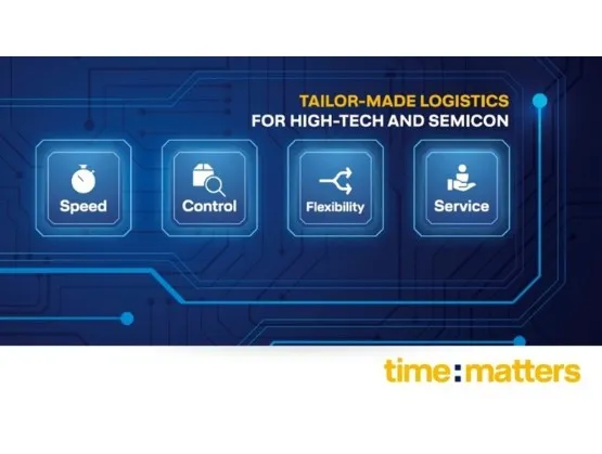
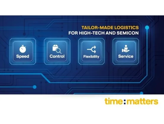
The New Reality of Semiconductor Supply ChainsThe semiconductor industry is one of the most globally connected and time-sensitive sectors in existence. From design and wafer fabrication to testing, assembly, and delivery, every step depends on flawless coordination across borders, suppliers, and time zones. More than 1 trillion chips move through global supply chains each year[1], connecting suppliers, foundries, and fabs across continents.But as the world becomes more complex and unpredictable – with trade tensions, capacity shortages, shifting technology cycles, and driven by increasing AI and energy demand – that coordination is increasingly under pressure. Even a minor delay in one place can halt production in another. A single missed component, delayed shipment, or grounded flight can trigger line-down costs that can exceed $4 million per hour in advanced fabs[2].That’s why logistics is no longer a background process; it’s a strategic function that directly influences performance, reputation, and profitability.Figure 1 - We live in a complex and unpredictable world where global events have significant impacts. When Every Hour MattersFew industries feel the impact of delays as directly as semiconductors. One missing component, a grounded flight, or a customs delay can trigger a chain reaction that stops production lines, delays product launches or breaks contractual commitments.Time-critical logistics plays a distinct role in safeguarding supply chain performance, staying in control and enabling companies to recover in hours instead of days. It serves as the system’s shock absorbers when conventional routes are disrupted, timelines collapse, or customer commitments are at risk.The ROI of UrgencyTime-critical shipments are costly—but in the semiconductor world, not acting fast is far more expensive and pose significant consequences. A single line-down event can cost millions of euros per day, depending on the process stage and the customer involved. Compared to that, the premium for a same-day or next-flight shipment is minimal.When companies integrate time-critical logistics as a planned capability, the ROI becomes tangible.Avoided downtime: Faster recovery after supply interruptions directly protects production yield and customer commitments.Reduced inventory buffers: If rapid response capacity is available, less working capital is tied up in safety stock.Customer retention: Reliable continuity strengthens trust and long-term business relationships.In this sense, time-critical logistics isn’t just an operational expense – it’s a continuity investment. It protects revenue streams and reputation and gives manufacturers the agility to respond to whatever the next disruption brings.Example scenarios include:A single fab tool delay can idle an entire production line, costing millions per hour. During the 2024 Taiwan earthquake, a single supplier delay triggered hundreds of millions in global production losses.A next-flight-out or onboard courier shipment typically represents less than 1% of that downtime cost.Rapid recovery also prevents ripple effects such as delayed customer deliveries.The companies that embed time-critical logistics as a strategic capability gain not only cost protection, but competitive agility.From Efficiency to AgilityTraditional supply chains were built for stability and scale: move high volumes, keep costs low, and plan far ahead. But in the semiconductor industry, speed and adaptability now define competitiveness.Agility means having the systems, partners, and mindset in place to act decisively when the unexpected happens. Leading companies are now integrating dedicated control towers, predictive data insights, and predefined emergency logistics playbooks – turning reaction time into a measurable performance indicator. However, agility is not only a matter of infrastructure – it depends on data-driven visibility and cross-industry collaboration.Collaboration as the Real DifferentiatorNo company can face disruption alone. Semiconductor supply chains depend on the combined coordination of equipment makers, material suppliers, foundries, logistics providers, and government agencies.Collaboration is therefore the new competitive edge. Shared standards, visibility tools, and coordinated crisis response frameworks – like those developed under the SEMI Supply Chain Management Initiative – are helping the industry build collective resilience. These cross-functional efforts are where innovation scales.Looking AheadThe semiconductor industry will continue to expand into new regions and technologies. Each step adds complexity and, with it, vulnerability. The next decade will test not just how fast companies can produce, but how fast they can recover. Future disruptions – whether geopolitical, environmental, or digital – are inevitable. The question is not how to avoid them, but how to respond faster and smarter when they occur.That’s where time-critical logistics will continue to make its mark. It is more than just a transport solution. It gives companies the ability to act decisively in moments that matter most – transforming time from a constraint into a competitive advantage that ensures business continuity.Key TakeawaysSemiconductor supply chains are uniquely time-sensitive — a single delay can halt multimillion-dollar production lines.Integrating time-critical logistics improves responsiveness, reduces inventory needs, and safeguards business continuity.Agility, not efficiency, will define the next decade of semiconductor competitiveness.Collaborative industry frameworks like the SEMI Supply Chain Management Initiative are key to building resilience.How ready is your supply chain?Learn more about time:matters’ tailored logistics solutions at SEMICON Europa 2025 (Hall C2, Booth 433), November 18-21 in Munich and attend the company’s presentation on the TechARENA stage on November 19. For more information or to schedule a meeting at SEMICON Europa, click here to contact Remy Schoenzetter.Remy Schoenzetter is Global Head of Business Unit High Tech Semicon at time:matters.[1] Statista: Global semiconductor unit shipments 2021; SIA/WSTS Annual Reports[2] McKinsey: "Need to boost semiconductor fab efficiency?" (2023); LinkedIn Air Monitor analysis (2025); Critical Manufacturing Industry Blog (2024)
Read More
The semiconductor and electronics industries are at a turning point. Once defined by efficiency and scale, supply chains now face a convergence of pressures—from geopolitical tensions and climate risks to accelerating innovation cycles. The stakes are higher than ever, but so are the opportunities to reimagine how this global ecosystem operates.The End of “Just-in-Time” as We Knew ItIn 2025, one thing is clear: the old “just-in-time, globally concentrated” supply chain model can no longer carry the industry forward. Trade policies are tightening, export controls are multiplying, and tariff investigations are fragmenting markets that once felt seamlessly connected.At the same time, natural resource risks are mounting. PwC estimates that by 2035, nearly one-third of global semiconductor production could face copper supply disruptions caused by climate change. That figure rises to nearly 60% by 2050 if emissions remain unchecked. Add to this the growing maze of regulatory barriers and import restrictions on raw materials, and the industry faces rising procurement challenges and relentless cost volatility.Demand Isn’t WaitingWhile supply chains struggle with constraints, demand continues its upward climb. Global chip sales are rebounding, driven by innovation cycles in AI, automotive electronics, 5G, and renewable energy. Bringing new manufacturing capacity online takes years. The imbalance is widening, and companies can’t afford to rely on outdated, reactive supply chain models.Resiliency has become mission critical. And as the saying goes: you can’t respond to risks you can’t see. Guesswork isn’t a strategy—especially when disruptions are systemic.Fragility in a Fragmented EcosystemSemiconductor production is specialized and geographically fragmented. A disruption at a single node—whether a mine, a fab, or a logistics hub—can ripple through the ecosystem in days or even hours.Recent shocks have only reinforced this fragility:Trade restrictions are pushing manufacturers to rethink supply chain design.Climate change is endangering raw materials like copper and quartz, both highly water- and energy-intensive to produce.Market volatility is being driven by the explosive rise of AI and data center demand.The lesson is simple: resilience is no longer optional—it’s an existential requirement. And the path to resilience runs through visibility, agility, and collective intelligence.Real-Time Intelligence: From Luxury to NecessityIn today’s environment, quarterly or even monthly reporting cycles are dangerously slow. By the time a shortage, tariff, or logistics reroute appears on the radar, the window to act may have already closed. The cost of waiting—or doing nothing—is steep, and the damage can be lasting.Real-time data and AI-driven insights aren’t “nice-to-have” tools anymore. They are strategic imperatives for supply chains under constant stress. They allow companies to anticipate risks, respond faster, and align more effectively with partners across the ecosystem.Collaboration Is the New CurrencyNo company can go it alone. A chipmaker depends on its suppliers, just as a rare earth miner depends on transport partners. The global supply chain is a living system—and its resilience depends on the strength of its interconnections.Deeper supplier relationships, visibility into Tier 2 and Tier 3 suppliers, and shared intelligence on geopolitical and regulatory shifts are all critical. Resiliency isn’t built in silos; it’s forged through collective action.Building the Future TogetherThe semiconductor and electronics industries stand at the threshold of a new era—one of collective risk but also shared potential. Companies that embrace transparency, real-time intelligence, and collaboration will not just survive shocks, but emerge stronger, more agile, and better prepared to lead.In this new chapter, collaboration is the currency of resilience.That’s where Conductor™ comes in: a real-time intelligence platform built to help industry players anticipate, adapt, and act – together. Conductor weaves all those threads together, delivering not just data, but a shared situational awareness, helping the industry to think and act as a system rather than a collection of silos.What Conductor Enables - and What It Could Lead ToSmarter, faster decisionsA platform like Conductor, which uses near real time data, AI-powered news and alerts, and community-driven insights, turns reactive “damage control” into proactive “risk management.”By bringing together cross-segment, critical KPIs, curated AI news, expert analysis, and peer-community intelligence, Conductor helps teams understand what’s happening now, assess the likely impact on their business, and decide how to respond - faster, and with more context.Over time, this could shift the default mode of the industry from “fire-fighting” to “anticipatory steering.”A more adaptive supply chainAs more organizations adopt the platform, the collective visibility improves. Conductor can power scenario planning, enable early warning systems, and foster agile “micro-pivot” strategies: reroute logistics, adapt sourcing, or reallocate production before a disruption becomes a crisis.New models of ecosystem resilienceWith consistent, shared intelligence, industry players can identify common vulnerabilities and coordinate mitigation for mutual gain. Over time, this could lead to more resilient operations through diversified sourcing strategies, and even shared contingency mechanisms.In short: Conductor is a building block toward a more distributed, more transparent, more resilient global semiconductor ecosystem.Accelerated innovation cyclesWhen the risk of disruption is better managed, companies can operate with more confidence, investing in new capacity, experimenting with new chip architectures, or integrating new markets more aggressively. Technology diffusion accelerates when the fear of “what-if” is reduced.Where We Go From HereConductor is already in early-access pilot phase, and feedback from the SEMI Supply Chain Management Initiative’s Industry Advisory Council is actively shaping its evolution.As adoption spreads, network effects will increase the platform’s predictive power, making it more valuable for everyone involved.In an industry that’s increasingly defined by fast change and high stakes, tools like Conductor shift the balance: from reactive scramble to informed strategy, opaque fragility to visible resilience, and from isolated action to ecosystem collaboration.The future of supply chain resilience starts here. Sign up for early access to Conductor today and help drive the new era of trade.Talal Abu-Issa is Co-CEO and Co-Founder of Beebolt.Krish Dharma is Strategic Advisor, SEMI Supply Chain Initiative.
Read More
Atomic layer deposition (ALD) and atomic layer etching (ALE) are transforming the way semiconductors are built—layer by layer, atom by atom. These atomic-scale processes are essential to scaling future transistors, improving memory, and enabling next-generation device architectures.SEMI spoke with Sergei Ivanov, Business Technology Director of Metallics R D and Balaji Kannan, Business Technology Director of Dielectrics R D and from Merck KGaA, Darmstadt, Germany to learn about their latest material innovations. At the company’s Electronics business, materials scientists and process engineers are advancing atomic-scale engineering to address some of the semiconductor industry’s toughest challenges. From novel deposition chemistries to next-generation etch techniques, their work is helping to enable future logic, memory, and specialty devices.Pushing the Boundaries of ALD Precursor ChemistryAtomic Layer Deposition (ALD) remains a cornerstone technology for scaling transistors and enabling new architectures. Materials scientists at Merck KGaA, Darmstadt, Germany are exploring novel precursors that enhance film quality, streamline processes, and expand the operational window for complex structures:One area of focus is next-generation hafnium and zirconium precursors. “These advanced high-k dielectrics offer better thermal stability, improved step coverage, and reduced impurities while achieving higher k-values,” Sergei Ivanov explained. “Such attributes are essential for logic and memory devices that demand reliable dielectric performance with minimal defect density.”Another important development is area selective deposition (ASD). Merck KGaA, Darmstadt, Germany’s small-molecule inhibitor solutions reduce the need for advanced patterning in narrow dimensions and 3D geometries, enabling cost-effective and simpler integration for leading-edge nodes. Their selective co-reactants platform leverages digitalization techniques including multivariate analysis, digital twin technology, and machine learning to accelerate process development for critical ASD applications. This approach facilitated industry-first adoption of ASD in high volume manufacturing and enables an ever-expanding toolbox of OEM processes for ASD of high-k, Ti, Mo, Si and other thin films.Merck KGaA, Darmstadt, Germany is also broadening the scope of ALD chemistries across the periodic table. “As our customers encounter new technical challenges, we continue to expand our R D scope across new elements and ligands. Examples include europium, lanthanum, scandium, and cerium dopants with improved electrical properties, niobium and vanadium precursors for deposition of nitride and oxide films with reduced impurities and improved ALD performance, and high-performance nickel MILC solutions are finding their way out of our labs and into customer roadmaps at an ever-accelerating pace,” said Sergei Ivanov.The company’s role in molybdenum chemistry is another example. Merck KGaA, Darmstadt, Germany is a key producer of molybdenum precursors including MoO2Cl2 with industry-leading quality, density, and container utilization. The company offers MoCl5 with advanced trace impurity control paired with innovative container technology. The company’s next-generation organic metallic molybdenum precursors incorporate novel ligands that contribute to critical gains in device performance.Merck KGaA, Darmstadt, Germany’s work with organosilane precursors is also opening new possibilities. “For gate-all-around (GAA) transistor technology, precursors incorporating novel bonding structures enable highly conformal dielectric films with excellent electrical and physical properties, even in complex 3D geometries. At the same time, organosilane chemistries designed to increase silicon incorporation during deposition are supporting high-growth-rate oxides for gapfill applications, delivering the thick films required with greater throughput,” said Balaji Kannan. “Together, these innovations highlight how tailored precursor design can address both scaling challenges and manufacturability in next-generation devices.” Driving Selective and Sustainable Atomic Layer Etching (ALE)“Precision in etching is as critical as deposition. Our innovations in ALE are designed to provide ultra-selective, low-damage material removal, which is increasingly vital as device geometries become finer and more complex,” Sergei Ivanov shared. One example is metal-free ligand exchange ALE for high-k materials, where Merck KGaA, Darmstadt, Germany’s research into etching HfO₂, ZrO₂, and HfZrO₄ showcases a novel metal-free approach. This technique enables accurate and damage-minimized etching of high-k dielectrics, which is essential for integrating advanced transistors and memory stacks.These advancements address industry-wide concerns regarding pattern fidelity, material selectivity, and plasma-induced damage, ensuring greater process control and extending the lifetimes of devices.Looking AheadMerck KGaA, Darmstadt, Germany’s strategic commitment to semiconductor innovation includes ongoing R D efforts that reflect the vision of its Electronics business: providing material-centric solutions to the industry’s most complex integration and performance challenges. Whether advancing front-end device scaling or developing breakthrough materials for emerging applications, the Electronics business of Merck KGaA, Darmstadt, Germany is committed to shaping the materials roadmap for a more connected, intelligent, and efficient world.James Lam is Business Development Manager at SEMI Europe.
Read More
The semiconductor industry faces an uncomfortable contradiction. Markets are expanding and demand continues rising, but the talent pool is shrinking.By 2030, the industry will need to add 1 million skilled workers globally, with shortages of over 100,000 engineers in Europe and more than 200,000 engineers in Asia-Pacific. This expansion requires at least 100,000 second-line leaders and 10,000 third-line leaders—many of whom must come from outside the industry.Markets Keep Growing, Leadership Doesn'tThe industry's outlook remains optimistic. Nearly one in five (19%) semiconductor executives anticipate continued demand growth without inventory excess in the next four years. Global sales hit $627.6 billion in 2024—a 19.1% increase driven by AI advancements, consumer electronics demand, 5G adoption, and automotive innovation.Governments are backing this growth with large investments too. The European Chips Act aims to double the EU's production share to 20% by 2030 with €43 billion. Companies like NXP Semiconductors, Infineon Technologies, and STMicroelectronics are expanding. Taiwan Semiconductor Manufacturing Company (TSMC) remains the world's largest contract chipmaker. The UK government unveiled a £1 billion strategy over 10 years, while the CHIPS and Science Act allocated $52.7 billion for US manufacturing and research.But there aren't enough semiconductor leaders to manage this growth.The Education CrisisThe talent shortage begins in universities. Electrical engineering and computer science enrollment has been declining for years. Germany saw 6.5% fewer STEM students in 2021 than the previous year.An analysis of recent data shows concerning patterns. While Germany had 81,934 electrical engineering students in 2018, Ireland had only 742 new electrical engineering students in 2017. The United States awarded just 13,767 bachelor's degrees in electrical engineering in 2018.Retirement and Skills GapsWhile universities produce fewer graduates, experienced leaders are retiring. One-third of US semiconductor employees are 55 or older. In Germany, one-third of the workforce will retire within the next decade.The job itself is also changing. Artificial intelligence and machine learning have surpassed systems architecture as the most sought-after skills in European markets. Software engineers specializing in embedded programming are becoming more important than traditional design engineers.Competition and TurnoverThe semiconductor industry competes with other tech sectors for talent, and ninety-two percent of tech leaders report challenges finding skilled workers.Employee turnover is accelerating as well. Fifty-three percent of semiconductor workers were expected to resign in early 2024, compared to 40% in 2021. Top reasons include lack of career development (34%) and insufficient workplace flexibility (33%).Geographic ChallengesManufacturing concentration creates additional problems. Taiwan handles 65% of global manufacturing, China 15%, South Korea 12%, and the US 12%. Despite this, U.S.-based companies hold roughly 46.3% of global market share.Each region has developed different skill sets, making it difficult to move leaders across markets.What Companies Are DoingAbout 60% of senior executives believe semiconductor companies have weak employer brands compared to higher-profile tech companies. Many are working to change this through competitive compensation, improved work-life balance, and better career opportunities.Some companies are expanding their search beyond traditional candidates, too. Seventy-three percent now use skills-based hiring, focusing on capability rather than traditional backgrounds. Others target adjacent tech sectors for executives with transferable skills.Retention has become more important as well. With the tech industry's 13.2% attrition rate, companies are investing in career progression and workplace flexibility.Diversity initiatives are also still gaining traction worldwide. Women represent only 17% of semiconductor tech roles, compared to 23% in the industrial sector.The semiconductor industry's future depends on solving this talent paradox. Companies that act decisively to attract, develop, and retain leadership talent will be best positioned to capitalize on market opportunities.About the AuthorJan-Bart Smits is Managing Partner at Stanton Chase Amsterdam and Global Subsector Leader for the Semiconductor industry.
Read More
The semiconductor industry is at the heart of modern technology, powering everything from smartphones and medical devices to communication systems and transportation. However, to sustain its rapid growth and innovation, the industry faces a pressing challenge: a growing talent gap. Addressing this issue requires collaboration between academia and industry to ensure that students are not only equipped with the necessary skills but also have clear pathways into the workforce.That’s where SEMI On Campus comes in. Launched in March 2025 by SEMI Europe, this new initiative is designed to bring together the semiconductor industry and universities, fostering collaboration that benefits students, educational institutions, and companies alike. With its first edition in Poland, SEMI On Campus is already making waves by reaching over 150 students and strengthening industry-academia connections.First Stop: PolandThe inaugural SEMI On Campus event took place at Gdańsk University of Technology and The University of Gdańsk, where key representatives from SEMI Europe—Bernard Capraro (Senior Manager, University Partnerships Talent Initiative), Victoria Cummings (Senior Manager, Workforce Development EU Projects), Maria Daniela Perez (Senior Manager, Business Development), and Kartikey Srivastava (Senior Specialist, Communications)—met with deans, professors, and students from various faculties.The Power of Industry-Academia CollaborationCollaboration between universities and the semiconductor industry is crucial in ensuring students gain practical knowledge, hands-on experience, and direct access to job opportunities. Companies, in turn, benefit from a steady pipeline of skilled graduates ready to drive innovation and meet industry demands.During the event, Bernard Capraro shared his own journey, from an engineering internship in Germany to leading research and development initiatives at Intel. His experience highlighted how diverse skill sets and career paths can lead to impactful roles in the semiconductor industry."Yes, the industry needs mechatronics engineers, data scientists, chemists, physicists, and computer science professionals. But it also needs media experts, gamers, biologists, environmentalists, public policy professionals, and communicators. It’s all about transferable skills and finding your area in this dynamic and diverse industry,” said Capraro.Expanding Opportunities with the European Chips Skills AcademyOne of the key initiatives supporting the semiconductor industry’s workforce development is the European Chips Skills Academy (ECSA). Designed to tackle skills shortages and propel industry growth, the Academy builds on the goals of the Microelectronics Pact for Skills and the EU Chips Act. With backing from 18 partners, including vocational training providers, research organizations, and industry leaders, ECSA aims to:Attract new talent into microelectronicsFoster collaboration between educational institutions and industryProvide training and certification opportunities to enhance workforce readinessVictoria Cummings emphasized how the initiative offers mentorship programs and access to leading companies and events. ECSA also builds on the student ambassador initiative, empowering institutions to support students in developing ideas and connecting them with mentors who can help shape their careers.Driving Diversity with the European Chips Diversity AllianceDiversity, equity, and inclusion are key to strengthening the semiconductor workforce. Kartikey Srivastava highlighted the European Chips Diversity Alliance (ECDA), a collaborative effort between academia and industry that aims to lower barriers to participation for underrepresented groups.With 11 partner organizations, the ECDA seeks to enhance inclusivity in the microelectronics sector, ensuring that the industry remains competitive and accessible to all. By fostering inclusive talent pipelines, the initiative is helping shape a more equitable and innovative future.A Successful Launch with a Bright FutureThe first SEMI On Campus event was a tremendous success, not only for the students who gained valuable insights and networking opportunities but also for universities and industry leaders looking to strengthen their collaboration. By building bridges between academia and industry, SEMI On Campus is paving the way for a more skilled and dynamic semiconductor workforce in Europe.If you’re interested in hosting a SEMI On Campus initiative or inviting an industry representative to speak at your institution, please reach out to [email protected]. Let’s work together to inspire the next generation of semiconductor leaders!SEMI Contact: Maria Daniela Perez, Senior Manager Business DevelopmentEmail: [email protected] Lam, Manager Business DevelopmentEmail: [email protected]
Read More
The Rising Stars: 20 Under 30 blog series celebrates the brightest young leaders shaping the future of the semiconductor industry. These exceptional individuals have earned the SEMI Europe 20 Under 30 Award for making a remarkable impact across the supply chain—whether in engineering, sales, marketing, or R D. Nominations for the 2025 20 Under 30 Award are now open, providing the opportunity to recognize and honor the next wave of industry trailblazers.The series spotlights these rising stars for their career achievements, commitment to innovation, leadership skills, and dedication to driving both business success and community growth.Follow their inspiring journeys and discover how they are thriving and paving the way for future generations in the semiconductor world.Introducing Mariusz Grabowski: Lead Design Engineer at Cadence Design SystemsMariusz Grabowski, a 2023 20 Under 30 award recipient at the age of 24. He is now a Lead Design Engineer at Cadence Design Systems, Inc., where he’s been making strides in digital systems design for nearly three years. Prior to this role, he gained valuable experience as an FPGA Design and Verification Engineer at Aldec Inc. Grabowski holds a master’s degree with distinction in automation and robotics from AGH University of Science and Technology in Krakow, Poland. During his academic career, he was an active member of both the Avader and Integra Scientific Groups. He also achieved recognition at events like DASIP 2023 and in the International FPGA Hackathon, where he and his team earned 2nd and 3rd place. He is currently also pursuing a postgraduate degree in Project Management at SGH Warsaw School of Economics. SEMI: What inspired you to join the semiconductor industry? Grabowski: I have always been fascinated by the fundamental workings of advanced systems and that curiosity led me to pursue a career in the semiconductor industry. As a digital design engineer, it is exciting for me to contribute to the creation of such large and sophisticated architectures from basic building blocks. Now, I’m proud to be a part of Cadence Design Systems, where I can work on the cutting-edge designs with some of the most talented and hard-working engineers. Grabowski and his team at the awards ceremony at FPGA Hackathon 2023SEMI: How did your early experiences and education shape your career path?Grabowski: During my studies, I had the opportunity to work on hands-on projects with an FPGA platform, which led me to my first job as an FPGA design and verification engineer. That experience gave me a broader perspective on the industry’s scale and reinforced my passion for tackling challenges, learning and growing in this field.Grabowski presenting his paper at the DASIP 2023 ConferenceSEMI: Can you share a professional accomplishment you’re most proud of, and explain why it’s significant to you? Grabowski: For me, it is successfully balancing full-time studies with work. It was a challenging experience, but it provided invaluable opportunities to grow my skills and gain hands-on experience. During that time, I completed numerous projects, participated in scientific conferences and industry events like DASIP 2023, and even earned 2nd and 3rd place in the International FPGA Hackathon. These achievements reinforced my passion for the field and my ability to thrive under pressure. SEMI: As a young professional in the industry, what is your greatest challenge? Grabowski: One of the biggest challenges is navigating the complexity of large-scale projects, where seamless coordination between multiple teams across the globe is crucial. As someone still early in my career, gaining the experience to manage the cross-functional aspects of a project while ensuring my own contributions are technically sound has been both demanding and rewarding.Grabowski at the Discussion Panel on Industry Career Perspectives at DATE 2024 ConferenceSEMI: What advice would you give to younger generations aspiring to make an impact in this industry?Grabowski: The sheer amount of information and complexity in the industry can feel overwhelming. It is essential to embrace curiosity and continuous learning, but it is also crucial to recognize that you can’t do everything alone. My advice is to find your area of expertise and collaborate with others; teamwork is key to bringing impactful projects to life. Cadence’s Design Team in Warsaw, Poland Manager Jacek Rosiak—3rd from the leftSEMI: How do you envision future work environments? Grabowski: I envision future work environments as places where technology fosters creativity and collaboration, diversity is celebrated, and flexibility and work-life balance are prioritized. These environments will empower employees to perform at their best while feeling supported and valued. I am proud to be a part of Cadence Design Systems, where I feel that these values are strongly cultivated. SEMI: What impact has the 20 Under 30 Award had on your career? Grabowski: Receiving the 20 Under 30 Award was an incredible validation of the hard work I’ve put into my role. It gave me a confidence boost, affirming that I am on the right path and capable of making meaningful contributions to my company and the broader semiconductor industry. It also brought significant recognition, which opens up numerous opportunities.Following 20 Under 30 JourneysMariusz Grabowski’s journey in the semiconductor industry highlights the power of dedication, curiosity, and continuous learning. From his early experiences with FPGA platforms to his significant accomplishments in both academia and industry, Grabowski is a true example of how passion and hard work can drive meaningful contributions. As a young professional, his insights offer valuable inspiration for the next generation of engineers eager to make their mark in this ever-evolving field. With a bright future ahead, Grabowski is sure to continue influencing the world of technology, one innovative project at a time.The Rising Stars: 20 Under 30 blog series celebrates the exceptional talent and leadership driving the future of the semiconductor industry. Each of the young innovators honored is excelling in their respective fields while shaping the landscape of technology and business with their visionary approaches and dedication. Their stories exemplify the remarkable achievements and unwavering commitment that define the next generation of industry leaders. The series is intended to inspire and motivate future professionals to pursue their passions and embrace the opportunities within this dynamic industry. Stay tuned for more stories of rising stars who are paving the way for continued growth and innovation in the semiconductor world.Learn more about the SEMI Europe 20 Under 30 Award and the recipients honored at SEMICON Europa. SEMI ContactMaria Daniela Perez, Communications ManagerEmail: [email protected]
Read More
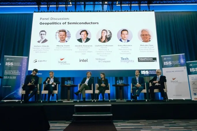
As geopolitical dynamics continue to influence global industries, the semiconductor sector finds itself at a pivotal crossroad. During the SEMI Industry Strategy Symposium (ISS Europe) held in Sopot, Poland, a high-level panel on the Geopolitics of Semiconductors brought together leaders from across the ecosystem to explore Europe’s role in an increasingly fragmented world shaped by strategic dependencies and evolving alliances.Moderated by Stefano Ramundo Orlando, Advocacy Manager at SEMI Europe, the panel convened industry executives, strategic advisors, and policy experts for a forward-looking dialogue on the challenges and opportunities shaping Europe’s semiconductor future.The session opened by acknowledging the rapidly changing geopolitical landscape and its impact on the global semiconductor supply chain. Export controls, investment screening mechanisms, and economic security strategies are no longer abstract policy discussions — they are reshaping investment decisions, manufacturing strategies, and even workforce planning across the globe. While these disruptions present undeniable challenges, panellists underscore that they also mark a pivotal opportunity. For Europe, this is not a moment to retreat but a call to adapt with purpose.Closing the Gaps: Building on Europe’s Strategic AdvantagesGiulietta Poltronieri, Partner at McKinsey Company, mapped out Europe’s strategic position in the global value chain. While Europe boasts global leadership in intellectual property (IP), lithography, and research and development (R D), key gaps remain in foundry capabilities and backend manufacturing. The solution lies not only in plugging these gaps but in securing Europe’s existing strengths — a balancing act between resilience and competitiveness.Giulietta Poltronieri, Partner, McKinsey Company’s Global Semiconductor PracticeMalcolm Penn, Founder CEO of Future Horizons, echoed this sentiment and emphasized that success in semiconductors requires long-term vision and a global mindset. Penn argued that Europe must look beyond its local market, citing Taiwan’s TSMC as a model of how small domestic markets need not constrain global leadership, “The excuse of having no end market in Europe is just an excuse.” Europe, Penn contended, must have the courage to think big and act boldly.Malcolm Penn, Founder Chief Executive Officer, Future Horizons Corporate Strategy Amid UncertaintyHendrik Bourgeois, Vice President of European Government Affairs at Intel, offered insight into how geopolitical risk has become an embedded factor in corporate strategy. Intel’s decision to expand manufacturing in both the U.S. and Europe was directly influenced by a recognition of over-reliance on certain global regions.Bourgeois stressed that while business can adapt to restrictive policy, uncertainty remains the greatest challenge to long-term decision-making. Consistency, trust, and engagement with governments are crucial — and businesses must invest in building political capital just as they do in infrastructure or talent.Hendrik Bourgeois, Vice President, European Government Affairs, Intel China: Partner, Competitor, and Geopolitical PuzzleBoris Metodiev, Director at TechInsights offered a balanced view of China’s role — acknowledging it as both a vital market and a strategic competitor. With nearly 40% of global semiconductor demand and significant state backing, China presents both irresistible opportunity and real systemic risks.Key concerns include technology transfer, the impact of heavy subsidization, and growing market concentration. Addressing these issues, Metodiev suggested, will require a balanced approach focused on diversifying supply chains, protecting intellectual property, and reinforcing trade enforcement — all while maintaining open channels for cooperation and avoiding the pitfalls of full decoupling.Boris Metodiev, Director, Manufacturing Analysis, TechInsights Talent: The Silent BottleneckPanellists identified talent shortages as one of the most yet under-discussed threats to Europe’s semiconductor future. Europe lacks the scale of skilled STEM graduates to meet current and projected demand.Companies like Intel are investing heavily in partnerships with universities and training institutions. However, regulatory obstacles — especially for intra-European mobility of non-EU nationals — remain significant. The call to action was clear: Europe must rethink migration and education policy through the lens of economic strategy, not just under traditional policy frameworks, aligning policy with industrial goals and scaling efforts to match future workforce needs.Central and Eastern Europe: Emerging Pillars of European StrategyThe panel explored how Central and Eastern Europe are increasingly integral to Europe’s semiconductor strategy. Mikołaj Trunin, Deputy Director at Invest in Pomerania, noted that despite geopolitical headwinds, the region continues to attract strong foreign direct investment (FDI). Poland has emerged as a trusted investment destination and a budding semiconductor hub, with Pomerania positioned as a key region for advanced packaging.With nations like Poland taking on higher political and industrial profiles—such as upcoming leadership of the EU Council— the region is positioned to serve as a strategic bridge between Europe’s industrial core and frontier markets. This momentum underscores the importance of embedding these regions more fully into the broader semiconductor ecosystem.Mikołaj Trunin, Deputy Director, Invest in Pomerania A Call for Coordinated ActionThe panel concluded on a note of clarity: geopolitical disruption is not a temporary deviation, but a defining characteristic of the coming industrial era. With semiconductors positioned at the intersection of technology, security, and sovereignty, Europe must act decisively. Companies must continue to evolve, engage politically, and remain agile. To ensure long-term competitiveness and resilience, policymakers and industry leaders must work hand in hand to shape an integrated European semiconductor ecosystem. The stakes are high — but so is the potential.SEMI ContactIranda Chaki, Senior Policy CoordinatorEmail: [email protected]
Read More
In a world where technological advancements move at lightning speed, the semiconductor industry is facing unprecedented challenges. The demand for smaller, faster, and more energy-efficient devices is growing, and traditional manufacturing processes are being pushed to their limits. Enter Spin-on Dielectrics (SOD), a breakthrough material technology that offers a cost-effective, scalable solution for micro-gap filling and high-performance dielectric films. As the industry evolves, SOD is expected to play a pivotal role in enabling the next generation of chips that power everything from AI to everyday electronics.To learn more, SEMI Europe and Merck KGaA, Darmstadt, Germany, held a joint webinar that focused on semiconductor device process evolution by SOD. The session featured insights from three technology experts in the company, including Dr. Surésh Rajaraman, Executive Vice President and Head of Thin Film Business Unit, along with Atsuko Yamamoto, R D Manager for Spin-On Dielectric, and Go Nakano, Global Marketing Manager for Dielectric Materials.SEMI: What is SOD, and how does it fit within the broader semiconductor manufacturing process?Rajaraman: SOD, Spin on Dielectrics, is a unique class of materials used to deposit thin layers of dielectric films, which act as insulators or other functional films, on semiconductor devices. The fabrication of a semiconductor chip involves thousands of intricate steps that incorporate conductors, semiconductors, and insulators. SOD is a versatile technology that supports device performance and miniaturization by enabling better gap fill and film uniformity, all while offering attractive cost of ownership.SEMI: Why is there so much focus on SOD materials, and how are they evolving to meet future industry demands?Rajaraman: As semiconductor devices become more complex—such as 3D NAND scaling to more than 300 layers and DRAM incorporating pillar capacitors—there’s a growing need for materials that can address challenges like interconnect delays, power consumption, and heat generation while maintaining optimal performance. Traditional dielectric materials are reaching their limits, making Spin-on Dielectrics (SOD) a critical solution. SOD offers advantages like bottom-up and seam-free gap filling, enabling ultra-thin insulating and other functional layers that enhance electrical and thermal efficiency and support next-generation device scaling.The industry is pushing the boundaries of scaling, with increasing aspect ratios and complex structures in Logic, 3D NAND and DRAM. Modern devices now require deposition in features which are not only incredibly narrow but also increasingly deep due to going into the third dimension. This creates new challenges, such as stress buildup and cracking in conventional SOD materials. To overcome this, we are developing enhanced formulations with improved mechanical stability and polymer backbone engineering. These innovations enhance gap-filling properties and resistance to process-induced stress, ensuring SOD remains a key enabler for advanced semiconductor manufacturing.SEMI: What are the current industry trends driving the adoption of SOD?Nakano: SOD is becoming a key technology because of its excellent gap-filling performance. Unlike gas-phase deposition methods like Chemical Vapor Deposition (CVD) and Atomic Layer Deposition (ALD), SOD is a liquid-phase process. This makes it more efficient for high-aspect-ratio structures. It also helps reduce costs while maintaining high-performance dielectric properties.With increasing demand for high-density memory and logic devices, SOD is crucial for applications like DRAM and NAND flash, which require precise dielectric layer formation. In DRAM, we’re witnessing a shift from planar to vertical transistors, and even to monolithic 3D DRAM. These changes require new materials for gate insulators and electrodes, alongside improvements in aspect ratio gap filling.For NAND memory, manufacturers are increasing the number of memory layers, leading to taller memory stacks and deeper trenches. As lateral scaling progresses, narrower and more complex structures demand high-aspect-ratio trench fills to maintain performance and reliability.Logic devices are also evolving, with transistor structures moving from FinFETs to nanosheets and forksheets. This transition enhances performance, but it also introduces challenges in wiring density and electrical properties. The narrower pitch of wiring requires advanced dielectric solutions, like SOD, to enable reliable, high-performance semiconductor architectures.SEMI: With all these recent innovations, what role does Merck KGaA, Darmstadt, Germany play in supporting these advancements, and what does the company offer its customers? Rajaraman: As the semiconductor industry pushes the boundaries of scaling, doing so requires materials that can support increasingly complex structures. We are the only materials company in the industry to possess the full spectrum of process technologies for gap-filling capabilities, including SOD, ALD, CVD, and Flowable CVD. Our strategic acquisition of Versum Materials has expanded our capabilities with organosilicon precursors. Combined with our SOD expertise, it allows us to reengineer material backbones with more material choices and tailored properties to optimize performance in high-aspect-ratio applications.To support this, we’ve expanded our global R D footprint. We now operate in various application labs, enabling close collaboration with customers for material customization and fine-tuning properties to address specific manufacturing challenges. Last year, we inaugurated a new R D center in Korea as part of our commitment to being near our customers and accelerating time-to-market for next-generation semiconductor solutions. As semiconductor roadmaps become more complex, customization and collaboration also become more critical. The key to innovation lies in working closely with our customers, understanding their challenges, refining materials, and optimizing processes together. By fostering this ongoing partnership, we can accelerate technological advancements and ensure that new solutions align seamlessly with evolving industry demands.SEMI: Can you share some technical insights on SOD?Yamamoto: SOD is a key material used in semiconductor manufacturing to create insulating layers with high precision. One of the essential components in SOD is PHPS (Perhydropolysilazane), a polymer composed of silicon, nitrogen, and hydrogen. This material is applied as a liquid solution and transforms into a high-quality silicon oxide film through a series of thermal processes.PHPS is essential because it enables precise gap filling in extremely small structures, helping to improve device reliability. The process involves spin-coating the polymer onto a wafer, followed by pre-baking to remove solvents. Then, it undergoes high temperature curing in an oxygen and steam atmosphere, forming a dense silicon oxide film. This method ensures uniform coverage and cost efficiency compared to traditional dry film deposition techniques.Our Spinfil® product line has evolved over the past two decades, starting with the Spinfil® 400 series and advancing through the Spinfil® 600 to the widely used Spinfil® 800 series. These improvements have enhanced gap-filling capabilities and film uniformity, making them ideal for high-aspect-ratio trench structures. The critical baking process involves spin coating and pre-baking before wafers undergo batch processing in a high-temperature furnace. Controlled temperature and moisture conditions transform Spinfil® into silicon oxide films, optimizing properties such as refractive index, shrinkage, and etching resistance and ensuring reliability in semiconductor applications.SEMI: What are the latest trends in new polymer development for SOD?Yamamoto: Our research focuses on three key areas: enhancing film quality, developing SOD for high-aspect-ratio trench filling, and advancing low-k SOD for semiconductor processes.To improve film quality, we introduced the Neofil®series, an evolution of the Spinfil® 800 series. This innovation reduces film shrinkage, lowers stress, and enhances wet etching rates, making it ideal for next-generation semiconductor nodes.Our latest Neofil® series for high-aspect-ratio trench filling is targeted for traditional dry processes like CVD and ALD, which can often lead to void formation and require multiple deposition-etch steps. Our latest SOD materials address this by improving polymer elasticity, ensuring uniform filling of deep trenches up to 16 microns without cracks, making them suitable for emerging 3D nanostaircase designs.In low-k SOD development, we’re focusing on siloxane-based polymers, which provide excellent trench-filling capabilities while maintaining strong mechanical and electrical properties. Compared to flowable CVD and ALD, SOD offers a more cost-effective and efficient alternative. With continued advancements, we anticipate SOD will become a key material for future semi-damascene processes, enhancing embedding performance and overall device reliability.SEMI ContactSitong He, Communications Manager Email: [email protected]
Read More