downloadGroupGroupnoun_press release_995423_000000 copyGroupnoun_Feed_96767_000000Group 19noun_pictures_1817522_000000Member company iconResource item iconStore item iconGroup 19Group 19noun_Photo_2085192_000000 Copynoun_presentation_2096081_000000Group 19Group Copy 7noun_webinar_692730_000000Path
Skip to main content
Default Banner Image

France

SANTA ROSA, Calif., – February 17, 2021 – PNI Sensor, the world’s foremost expert in precision location, motion tracking, and fusion of sensor systems into real-world applications, today announced availability of the new TargetPoint TCM™ gyro-stabilized digital magnetic compass. TargetPoint TCM incorporates PNI’s high sensitivity Magneto-Inductive sensors with the latest high stability 3-axis MEMS accelerometer and 3-axis MEMS gyroscopes providing accurate orientation while in dynamic motion and in magnetically challenging environments. TargetPoint TCM excels in conditions that cause errors in traditional digital magnetic compasses.

TargetPoint TCM uses advanced magnetic distortion compensation and calibration scoring algorithms to counter the effects of hard and soft iron interference, providing highly accurate heading information in almost any environment and orientation.

TargetPoint TCM features and benefits include:
 Patented magnetic anomaly rejection algorithms eliminate errors due to magnetic distortion, even in magnetically harsh environments
 Gyro-stabilized compass for dynamic accuracy of sub-0.5 degrees of heading accuracy
 Multiple calibration methods, including 12-point hard- and soft-iron calibration methods, are available to ensure ease of calibration for all applications
 ITAR-free

“For military rangefinder and targeting systems developers who need accurate orientation in demanding conditions, TargetPoint TCM is a ruggedized digital magnetic compass built to handle weapons shock,” said Robin Stoecker, vice president of sales and marketing at PNI Sensor. “It’s an ideal choice for targeting applications that require reliability, consistency and accuracy.”

Pricing and Availability
For product specifications, download the TargetPoint TCM product sheet. For pricing and availability, please contact PNI Sales or your regional PNI representative.

About PNI Sensor
With over 30 years of experience, PNI is the world’s foremost expert in precision location, motion tracking, and fusion of sensor systems into real-world applications. PNI’s sensors and algorithms serve as the cornerstone of successful IoT projects and other mission-critical applications where pinpoint location, accuracy, and low power consumption are essential. Building on decades of patented sensor and algorithm development, PNI offers the industry’s highest-performance geomagnetic sensor in its class, location and motion coprocessors, high-performance modules, sensor fusion algorithms, and complete sensor systems. To learn more, please visit www.pnicorp.com.

Media Contact:
Robin Stoecker
PNI Sensor
Tel: +1 707-566-2260 |Email: [email protected]

BERLIN, Germany – 17 February, 2021 –Qurv and Infineon Technologies have won the MEMS & Imaging Sensors Technology Showcase at the Technology Unites Global Summit, SEMI announced today. The Qurv wide-spectrum image sensor was recognized as the best imaging technology and the Infineon Technologies environmental sensor as the leading MEMS technology. The winners were selected from five finalists in each category in a vote by a committee of industry experts.

“Image and MEMS sensors advances are delivering tremendous societal and economic benefits, making our lives safer and healthier and the air cleaner,” said Laith Altimime, president of SEMI Europe. “The Qurv and Infineon Technologies innovations epitomize electronics industry innovation.”

The Technology Showcase honors standout applications enabled by MEMS and image sensors technology. The awards were presented by Dr. Martina Vogel of Fraunhofer ENAS.

Technology Showcase Winners

 Qurv Enabling a World of Enhanced Vision

Qurv developed wide spectrum image sensors that capture information hidden by ambient light interference or information not available in the visible light spectrum for next-gen computer vision applications. Qurv's technology leverages current CMOS scalable manufacturing and advanced materials to unlock new levels of performance, reliability and function. All Qurv image sensors are designed with AI and machine perception in mind. The technology was presented by Stijn Goossens, Co-founder and CTO of Qurv.

Qurv logo


Infineon TechnologiesXENSIV™ PAS CO2 Sensor, a new Environmental Sensor Technology. Photoacoustic Spectroscopy (PAS) Miniaturizes CO2 Sensors for High-volume Applications

Leveraging its advanced MEMS microphone technology, Infineon Technologies developed a disruptive CO2 sensor based on photoacoustic spectroscopy (PAS). Exceptionally miniaturized, the sensor is designed to accommodate high-volume manufacturing. The first CO2 sensor with SMD capabilities, the innovation will enable widespread adoption of air quality monitoring in high-volume applications in a variety of markets such as industrial, medical and Internet of Things (IoT). The platform was presented by Andreas Kopetz, Senior Director of Environmental Sensing at Infineon Technologies.  

Infineon Logo


The Technology Showcase demonstrations are available for on-demand viewing. The awards, organized by SEMI, are offered each year for companies across a range of sectors from IoT and consumer electronics to robotics and biomedical equipment. Winners receive a free exhibition booth at SEMI MEMS & Imaging Sensors Summit.

Technology Showcase Finalists

Stay in touch on Twitter and LinkedIn @SEMIEurope: #TechnologyUnites #SEMIEurope #SensorsSummit #MEMS #Imaging

About SEMI
SEMI® connects more than 2,400 member companies and 1.3 million professionals worldwide to advance the technology and business of electronics design and manufacturing. SEMI members are responsible for the innovations in materials, design, equipment, software, devices, and services that enable smarter, faster, more powerful, and more affordable electronic products. Electronic System Design Alliance (ESD Alliance), FlexTech, the Fab Owners Alliance (FOA) and the MEMS & Sensors Industry Group (MSIG) are SEMI Strategic Association Partners, defined communities within SEMI focused on specific technologies. Visit www.semi.org to learn more, contact one of our worldwide offices, and connect with SEMI on LinkedIn and Twitter.

Association Contact
Serena Brischetto/SEMI Europe
Phone: +49 30 3030 8077-11
Email: [email protected]
www.semi.org/eu


Semiconductor equipment manufacturer ClassOne Technology has just released its proprietary new SoftSeal™ Plating Rotor, designed to enhance processing performance on the company’s Solstice® electroplating systems. The announcement was made by ClassOne’s CEO, Byron Exarcos and Senior Technology Director, John Ghekiere.

“Together with the plating reactor, the plating rotor design is key to maximizing on-wafer performance,” said Exarcos. “It’s responsible for distributing the electrical supply across the wafer, isolating electrolytes from the electrical contacts, and a great deal more. Which is why we’re constantly working to optimize rotor performance. The new SoftSeal is our latest and most advanced generation in Solstice rotors, and it’s already achieving unprecedented levels of electroplating uniformity along with reduced cost of ownership.”

“This highly-uniform performance comes from a combination of finely-tuned rotating-disk electrode physics and an optimized density of electrical contacts around the wafer,” said Ghekiere. "The ‘SoftSeal’ name comes from its high-performance FFKM elastomer seal which very effectively isolates plating chemistries from the wafer’s edge-exclusion zone. The new rotor also adapts automatically to substrate thickness, so it can accept thick or thin substrates without any adjustment. The design accommodates both flatted and multi-flat wafers, and it’s customizable to non-standard wafer sizes. Plus, the seal is more robust than on competitive rotors, meaning longer part life and no handling concerns.”

“In addition, the SoftSeal rotor’s low profile enables bubble-free entry into the plating bath,” Ghekiere noted. “And a unique design feature directs excess chemistry back into the bath at the end of the plating process. This is particularly important for conserving expensive plating baths such as gold. And, after processing, a special wafer retrieval method eliminates wafer flexing and stress by eliminating the need for extraction force at the center of the wafer.”

ClassOne stated that the new SoftSeal rotor is designed to fit all models of the company's Solstice electroplating systems and it will be standard equipment on all of the new tools going forward.

ClassOne Solstice systems are designed to provide high-performance, cost-efficient, single-wafer electroplating specifically for ≤200mm processing. The series includes the Solstice S8 and Solstice S4 for fully automated 8-chamber and 4-chamber high-speed production. It also includes the semiautomated Solstice LT, with up to three chambers that can be used both for process development and production. In addition to electroplating, the unique Plating-Plus™ capabilities of the Solstice platform enable it to handle many other important surface preparation functions, such as wafer cleaning, high-pressure metal lift-off, resist strip, UBM etch, and more. Class-leading performance and flexibility consistently make Solstice the tool of choice for ≤200mm plating across a range of product categories.

BERLIN, Germany ─ February 15, 2021 ─ The Catholic University of Leuven, Technical University of Dresden and CEA-Leti have won the 2019 European SEMI Award at the SEMI Technology Unites Global Summit for their pivotal contributions in the fields of telecommunications and nanotechnology. The award winners’ pioneering research and collaboration with academia and industry led to major advances in semiconductor technologies and their market adoption.

TUGS Logo

The European SEMI Award, established 32 years ago, recognizes key players in the global manufacturing supply chain for their leadership excellence and strategic contributions that help drive critical advances in the microelectronics industry.

2019 SEMI European Award Winners

  • Willy Sansen, Professor in Engineering Science at the Catholic University of Leuven (KU Leuven) and Gerhard Fettweis, Professor in Communications Engineering and Vodafone Chair at the Technical University of Dresden (TU Dresden),made outstanding research contributions in analog design and digital design techniques for a wide variety of applications.
     
  • Jean-Frédéric Clerc, Vice President, Technological Research Division of CEA-Leti, Grenoble-based French Alternative Energies and Atomic Energy Commission, received the European SEMI Special Service Award 2019 for outstanding research in nanotechnologies and contributions to the European semiconductor community throughout his career. With hundreds of patents to his name, Clerc drove research that led to innovations in liquid crystal flat screens and microsystems and is contributing to the development of biochips.

Winner Profiles

Willy Sansen


Willy Sansen, the Catholic University of Leuven

Since 1980 Sansen has served as full professor at the KU Leuven, where he has headed the ESAT-MICAS laboratory on analog design since 1984.
He has supervised 63 Ph.D. theses and authored or coauthored more than 635 publications and 16 books. He is a Fellow of the IEEE, was program chair of the ISSCC-2002 conference and is a Past-President of IEEE Solid-State Circuits.

Catholic University of Leuven Logo


Gerhard Fettweis Photo


Gerhard Fettweis, the Technical University of Dresden, and Barkhausen Institut

Fettweis has coordinated the Cluster of Excellence Center for Advancing Electronics Dresden and the Deutsche Forschungsgemeinschaft (DFG, German Research Foundation) Highly Adaptive Energy Efficient Computing (HAEC) for the TU Dresden since 2012. He founded the 5G Lab Germany in 2014, and among 12 startups Systemonic AG in 1999 and Signalion in 2003.

Technical University of Dresden Logo


Barkhausen Institut logo
Jean-Frédéric Clerc photo


Jean-Frédéric Clerc, CEA-Leti

Clerc was as an engineer at CEA-Leti from 1977 to 1984 and later became group leader at CEA-Leti. He worked as Research and Process Development Manager at Pixtech, a CEA-Leti startup, and served as CEA-Leti deputy Director at CEA-Leti and as Deputy Director of Division of Technological Research head of Division for Strategy and Programs.

CEA-Leti logo


Prior European SEMI Award recipients hailed from companies including STMicroelectronics, EV Group, Infineon, imec, Semilab, Deutsche Solar and the Fraunhofer Institute.

See the list of past SEMI European Award recipients. Nominations for the 2020 contributions are now open. To participate, please check the award guidelines online.


About SEMI
SEMI® connects more than 2,400 member companies and 1.3 million professionals worldwide to advance the technology and business of electronics design and manufacturing. SEMI members are responsible for the innovations in materials, design, equipment, software, devices, and services that enable smarter, faster, more powerful, and more affordable electronic products. Electronic System Design Alliance (ESD Alliance), FlexTech, the Fab Owners Alliance (FOA) and the MEMS & Sensors Industry Group (MSIG) are SEMI Strategic Technology Communities, defined communities within SEMI focused on specific technologies. Visit www.semi.org to learn more, contact one of our worldwide offices, and connect with SEMI on LinkedIn and Twitter.

Association Contact
Serena Brischetto/SEMI Europe
Phone: +49 30 3030 8077-11
Email: [email protected]
www.semi.org/eu


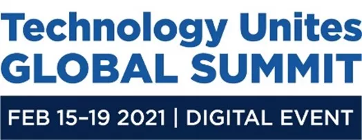
BERLIN, Germany – 15 February, 2021 – SEMI Technology Unites Global Summit opens today with keynotes on the power of technology to unite the world and insights on how the microelectronics industry can enable a secure and sustainable digital future. 15-19 February, the virtual event connects industry leaders and stakeholders across the entire electronics design and manufacturing value chain for the latest developments, trends, and innovations in key areas of industry growth including smart mobility, smart medtech, and MEMS and sensors. Registration is open.

TUGS LogoAt the opening day Executive Forum, international technology leaders will offer insights into the future of smart technologies as industry stakeholders gather to help shape the digital future for societal and economic prosperity.

Innovations across smart technologies such as 5G, artificial intelligence (AI) and Internet of Things (IoT) and industries including healthcare and mobility are transforming the way people work and live. The summit enables connections and partnerships while highlighting market opportunities in the digital transformation.

“While the past year brought tremendous societal and geopolitical challenges, it showcased the important contributions technology is making to improve all our lives, keeping us connected and working while accelerating the path to vaccines,” said Ajit Manocha, SEMI president and CEO. “The SEMI Technology Unites Global Summit will share insights from some of the microelectronics industry’s brightest minds on technology trends critical to advancing social and economic prosperity – and to staying ahead of the pace of digital transformation.”

Technology Unites Global Summit Highlights

  • Executive Forum
    • Global thought leaders will enable connections and partnerships and illuminate market opportunities for creating a smart, sustainable future. The executive forum will feature keynotes by executives from Infineon Technologies, imec, CEA-Leti, TEL, TSMC, NXP Semiconductors, Google, Umicore, JSR Corporation, Alibaba, Comet, Edwards Vacuum, AEM and UTAC.
       
  • Global Reach
    • The digital international exhibition will showcase new products and technologies while inviting interactions with a global audience.
    • Easy-to-navigate platform with opportunities for attendees to select content matching their professional interests and connect with like-minded industry experts.
       
  • Programs and Hosted Sessions
    • The Technology Unites Global Summit will highlight technologies and applications across key pillars of the next wave of microelectronics industry innovation and growth including mobility, advanced packaging, medtech, fab management, manufacturing, MEMS and sensors, advocacy, and diversity and inclusion.
    • Hosted sessions will provide the latest insights in start-up best practices, heterogeneous integration, smart manufacturing processes and standards, electronic systems design (ESD), advanced technologies, hardware for next-generation computing (NGC), ALD technologies, environmental sensors, and wet-chemical surface treatments.
       
  • Networking
    • Attendees will have direct access to technology leaders for answers to pressing questions.
    • Attendees will also enjoy opportunities to network with speakers, participants and customers through meet-the-expert sessions, live chats and video meetings.
       
  • Workforce Development
    • Those interested in careers in microelectronics will be able to tap current job vacancies in the industry.

Registration for the Technology Unites Global Summit for on-demand viewing of all content is open until March 26, 2021. The all-in-pass provides access to the entire event including forums, pavilions and the exhibition. Students, engineers, and startups can register at a special price.

Visit www.technologyunites.org or contact [email protected] for more information.

Follow #TechnologyUnites @SEMIEurope on LinkedIn and Twitter.   

  
Technology Unites Global Summit Premium Sponsors

Platinum 
ASE Group, CyberOptics Corporation, INFICON, Infineon Technologies, MADEin4, METIS, Picosun Oy, RENA Technologies GmbH, SPTS Technologies, a KLA company

Gold
AP&S International GmbH, Beneq Oy, Edwards Vacuum, EV Group, JSR Corporation, Merck KGaA, Darmstadt, Germany, Semics Inc., SÜSS MicroTec, Tokyo Electron Limited

Silver 
Comet, Evatec AG, FUJIFILM Electronic Materials, Okmetic Oy, SPEA Automatic Test Equipment, VAT Group 

Event sponsors: Advantest, Airspace, Applied Materials, CNW, DAS Environmental Expert GmbH, DB Schenker, Fraunhofer Institute for Photonic Microsystems IPMS, imec, Infinitesima, Lam Research, Max Group, PEER Group, Pfeiffer Vacuum, Posas GmbH, TRUMPF Hüttinger, Trymax Semiconductor Equipment BV, Watlow


About SEMI
SEMI® connects more than 2,400 member companies and 1.3 million professionals worldwide to advance the technology and business of electronics design and manufacturing. SEMI members are responsible for the innovations in materials, design, equipment, software, devices, and services that enable smarter, faster, more powerful, and more affordable electronic products. Electronic System Design Alliance (ESD Alliance), FlexTech, the Fab Owners Alliance (FOA) and the MEMS & Sensors Industry Group (MSIG) are SEMI Strategic Technology Communities, defined communities within SEMI focused on specific technologies. Visit www.semi.org to learn more, contact one of our worldwide offices, and connect with SEMI on LinkedIn and Twitter.

Association Contact
Serena Brischetto/SEMI Europe
Phone: +49 30 3030 8077-11
Email: [email protected]
www.semi.org/eu

ECM Lab Solutions is a new offer from the ECM Group, dedicated to laboratories, research centers and universities. This offer combines equipment from three companies and four brands: ECM Technologies, ECM Greentech, SEMCO Technologies & Cyberstar.

With more than 90 years of experience in manufacturing industrial equipment, this ECM Group offer highlights the diverse and flexbile nature of ECM's technology and expertise by transitioning from heat treating steels and automotive applications to a wide range of research and specialty fields.

With advanced technologies for crystal growth, vacuum heat treatment and chemical vapor deposition, ECM Lab Solutions offers reliable solutions for semiconductor, solar, medical and other mechanical applications.

Registration Details

Member Price: $99.00

Note:  Use company email address to log in for automatic recognition as a member.  Members must be current SEMI Members for member discounts.

Non-Member Price: $199.00

Belgium China France Germany Ireland Italy Japan Malaysia Singapore South Korea Taiwan United States Vietnam Register Now F47 Ad Business Technical
Advanced Energy
AMSC
Omniverter logo wtag

During the workshop recording, you will hear perspectives from the key stakeholder segments and develop a greater understanding of the overall efforts and progress of the task force.

The workshop is focused on diagnosing and improving SEMI F47, Specification for Semiconductor Processing Equipment Voltage Sag Immunity, widely adopted across the industry, the governing standard that defines voltage sag test levels and requirements for semiconductor tools.

Since the implementation of SEMI F47, the vulnerability of semiconductor manufacturing to single-phase and two-phase voltage sags has improved greatly. However, semiconductor manufacturers continue to experience significant product loss and downtime due to voltage sag events.

Given the ongoing issues with semiconductor plant downtime, a new SEMI Voltage Sag Immunity Task Force was formed to take a fresh look at the issue. The workshop and the task force:

  • Reviews the characteristics of the power quality events that cause downtime.
  • Takes a new look at the sensitivities in the process equipment.
  • Determines any potential adjustments to equipment design, facility design, utility systems, or SEMI Standards to further reduce voltage sag induced losses by the semiconductor industry.

Speaker Biographies

United States

10:00 am - 10:05 am
James Amano
James Amano
Sr. Director, Standards
SEMI

Welcome

10:05 am - 10:25 am
Mark Stephens EPRI
Mark Stephens
Principal Project Manager & Leader, Voltage Sag Immunity Task Force
EPRI

Introduction to the SEMI Voltage Sag Immunity Task Force Effort

A review of the key objectives of the voltage sag task force will be discussed along with the characteristics of the power quality events that are still causing semiconductor plant process downtime. A new look at the sensitivities in the tooling and process equipment is required to determine any potential adjustments to equipment design, facility design, utility systems or standards to further reduce voltage sag induced losses by the semiconductor industry. This important work will help utilities, semiconductor manufacturers, and tool equipment providers to better understand the tolerance and susceptibility of today’s generation of semiconductor processing tools and then to develop effective strategies to improve uptime and lower product losses due not only to single-phase (Type I) and two-phase (Type II) voltage sag events but for three-phase (Type III) events as well.

10:25 am - 10:50 am
Clay Burns
Clayton Burns
Principal Engineer
National Grid

Regional Voltage Sags- Importance of Addressing Three-Phase Voltage Sags in SEMI F47

A review of voltage sags at a National Grid substation which were produced by two lightning-caused three-phase transmission faults at locations fairly remote to the substation.  This will show the regional effect of transmission level faults on voltage.  The voltage sags will be compared to the existing SEMI-F47 standard and the accepted sag definition.  Additionally, a proposed regional voltage sag study will be considered in light of the changing make-up of the future electric system and the influx of large inverter-based resources.

10:50 am - 11:15 am
Ed McGann
Ed McGann
Manager of Engineering
VELCO

Utility Dynamic VAR device fault response, fault mitigation techniques, and power quality measures addressed with protection design

Co- presenters:
Greg Rieder, GlobalFoundries
Josh Burroughs, VELCO
John Fiske, VELCO

VELCO recently conducted a refurbishment of its STATCOM facility as part of a planned controls system upgrade. The system planning need for this facility is to provide area voltage support during transmission system contingencies. The refurbishment project team recognized the benefits of the STATCOM’s ability to provide voltage support during system faults and specified fault performance requirements in the vendor specifications. This presentation will discuss those performance requirements, review pre and post project upgrade system fault record’s and review project lessons learned. The second half of the presentation will cover utility fault mitigation design strategies for substation and transmission line assets as well as protective relaying techniques to improve power quality

11:15 am - 11:50 am
Michael Noth Austin Energy
Michael Noth
Power System Managing Engineer
Austin Energy

Seeing it from both sides: The importance of Power Quality Metering at the utility and inside the Fab Distribution System.

In this presentation we will discuss the importance of having power quality-based metering on both sides of the point of connection and other parts of the distribution system.  Mike will share some examples and stories of how important that can be.

11:50 am - 12:15 pm
Tony Sabin DAn Hunt
Dan Sabin & Tony Hunt
Schneider Electric

Waveform captures of voltage sag events can be automatically analyzed by software to determine their source and impact

This presentation will summarize efforts to categorize events automatically that exceed SEMI F47 limits, and to determine the source of those disturbances. It will also present recent efforts to analyze the impact of voltage sags automatically on electrical loads. This research has resulted in automatic algorithms to determine which voltage sags caused downtime and which ones did not. Combining all of this information together provides a means to more precisely and effectively diagnose, manage, and mitigate voltage sag disturbances.

12:15 pm - 12:25 pm
Christopher "Dale" Moffitt
Electrical Systems Engineering
HP

Power Quality and Monitoring, What Does the Data Tell Us?

Power Quality (PQ) has a long and diverse history dating back to the first power grids in the United States. Impacts and concerns about PQ events have evolved and will continue to evolve as our usage of electricity changes. Recent natural disasters have highlighted the importance of a robust power grid and the changing landscape of power generation presents new PQ challenges. As power consumers, a key element in any PQ strategy is adequate power monitoring. This provides the data that can drive conversation with the utility, discover opportunities in our infrastructure and deliver to our facilities the power quality necessary to sustain our businesses.

12:25 pm - 12:50 pm
Willem Meijs ASML
Willem Meijs & Giel Croonen
Low Voltage expert in electrical engineering on supply distribution system for machines
ASML

SEMI F47 and Power Quality Perspectives and Considerations from a Tool OEM

This presentation will address power quality perspectives and consideration from the point of a lithographic tools manufacture. Effect of different test methods on the sag immunity, test strategy on systems, sub-systems and components. How to divide a large installation up in to testable units and maintaining performance integrity. 3 phase type III test generator topology and the impact on harmonic emission and immunity in relation to voltage sag immunity.

12:50 pm - 1:15 pm
Josh Pankratz Advanced Energy
Josh Pankratz
Director of Engineering
Advanced Energy, Inc.

Power Supply Considerations and Standards for Voltage Sag Ride Through

Disturbances in utility power during semiconductor manufacturing can result in loss of revenue, productivity, production yields, and product quality. Focus on power quality continues to grow as new fabs are built in developing regions, which historically suffer from poor infrastructure. Highly automated fabs have driven a demand for systems that can ride through power glitches without shutting down tools and production lines. This presentation examines how power quality, most typically resulting in voltage sag events, affects semiconductor manufacturing and how industry standards and guidelines for tool immunity to those events affect the design of power supplies.

1:15 pm - 1:40 pm
Steve Lewis, Lam Research, square
Steve Lewis
Lam Research

Round Table Discussion & Q&A

1:40 pm - 1:55 pm
Mark Stephens EPRI
Mark Stephens
Principal Project Manager
EPRI

Next Steps for SEMI Voltage Sag Immunity Task Force

Based on the initial findings from utility and fab power quality data, the task force is poised to move forward to re-evaluate semiconductor tools against voltage sag additional characteristics that are indicative of measured events still causing downtime. Utilities, semiconductor fabs and equipment OEMs will be invited to actively participate in this effort to obtain the required test data.

1:55 pm - 2:00 pm

Closing Remarks & Adjourn

James Amano, SEMI

CAST FlexTech FOA ITL MSIG SCIS SE&A Standards EPRI and SEMI logos

SEMI & EPRI invite you to view a workshop held on April 21, 2021, to hear perspectives from all stakeholders on a persistent and difficult issue in microelectronics manufacturing - uncertain power quality. As work on SEMI Standard F47, the Specification for Semiconductor Processing Voltage Sag Immunity, continues this is the opportunity to hear from distinct parts of the supply chain. 

10:00 am - 2:00 pm Off Add to Calendar 2021-04-21 10:00:00 2021-04-21 14:00:00 Voltage Sag Workshop for Manufacturing Fabs SEMI & EPRI invite you to view a workshop held on April 21, 2021, to hear perspectives from all stakeholders on a persistent and difficult issue in microelectronics manufacturing - uncertain power quality. As work on SEMI Standard F47, the Specification for Semiconductor Processing Voltage Sag Immunity, continues this is the opportunity to hear from distinct parts of the supply chain.  United States SEMI.org [email protected] America/Los_Angeles public America/Los_Angeles
Event format

ClassOne Technology, global supplier of high-performance semiconductor electroplating and surface preparation systems, announced the sale of its Solstice® S8 system to South Korean chip manufacturer, Point Engineering Co. The eight-chambered Solstice plating tool will be installed at Point Engineering’s manufacturing facility in Asan City, South Korea. The announcement was made by ClassOne‘s CEO, Byron Exarcos, and PEC‘s CEO, Bum-Mo Ahn.

"Our products call for unique manufacturing approaches,” said Bum-Mo. “In addition to copper, we require plating of palladium cobalt alloy into highly variant features; and this plating is done on a proprietary substrate. We needed a volume-manufacturing platform that has the necessary flexibility without sacrificing reliability. The Solstice S8 covers these needs very well, and it also has a compact footprint to conserve fab space."

Exarcos pointed out that Point Engineering's new Solstice configuration includes a CopperMax™ processing chamber, a ClassOne-proprietary feature specifically designed to optimize copper plating. The chamber enables consistent high-quality, high-rate copper plating, while maximizing uptime and dramatically reducing bottom-line operating costs.

“Point Engineering has gained considerable respect in the industry for its semiconductor parts, which frequently go into probe pins and micro power inductors," said Exarcos. “In today’s semiconductor industry, we’re seeing that new product categories often drive the need for novel approaches in manufacturing. Point Engineering’s groundbreaking new products demand a process-experienced equipment provider and a flexible platform. We’re gratified that Point Engineering has chosen ClassOne and Solstice to partner with them on their next-generation products.”

The Solstice S8 is an 8-chambered system designed and built by ClassOne for high-performance, fully-automated electroplating and surface preparation, specifically for ≤200mm semiconductor wafer processing. The Solstice series also includes the S4, which provides up to four processing chambers, and the LT, with up to three chambers. In addition to electroplating, Solstice systems also provide Plating-Plus™ surface preparation capabilities, including wafer cleaning, high-pressure metal lift-off, resist strip, UBM etch and more. This multi-processing flexibility allows users to streamline wafer production and increase cost efficiencies by reducing the number of different processing tools required in the fab.

Villach, Austria, 20 Jan 2021 — mechatronic systemtechnik, a leading global supplier of automation equipment for semiconductor wafer handling, today announces the availability of the mWL.cs mechatronic calotte loader. A fully automated stand-alone system for transferring wafers between cassettes and calottes, the mWL.cs provides integrated device manufacturers (IDMs) an opportunity to increase yield and improve process traceability at a high throughput.

Evaporation process tools often utilize spherical carriers and rings to meet uniformity and defectivity targets. However, the design of these tools has made it challenging to introduce automated wafer handling in this step of the manufacturing process. IDMs invariably default to manual wafer loading, which has resulted in yield degradation and an increased risk for misprocessing.

“Automating the wafer loading and unloading system for evaporation type metal deposition is a step that bears much potential,” shared Stefan Detterbeck, Sales Director. “By eliminating human error from the equation, our system enables manufacturers to achieve higher yield and reduce damage to wafers. Enhanced process traceability also supports quality improvement measures to meet the conformity requirements of critical customer industries.”

Key features of the mWL.cs mechatronic calotte loader include:
 Superior handling accuracy and repeatability — hand-off position measurement and auto-teaching capabilities (About mechatronic systemtechnik
mechatronic systemtechnik, headquartered in Villach, Austria, is a leading global supplier of automation equipment for semiconductor wafer handling. Founded in 1998, the company specializes in addressing the industry’s needs for reliable, safe, and fully automated handling of non-standard substrates — including stacked, thin, or warped wafers, and also eWLP, MEMS, TAIKO, bumped, and film frames. Through a modular approach, mechatronic offers its customers cost-efficient handling systems that feature its proprietary technology. These solutions are capable of accommodating a wide range of substrate types and their specific characteristics. Major OEMs and fabrication plants across the globe rely on mechatronic’s unique solutions for some of their most complex wafer handling needs.

For more information, please visit www.mechatronic.at or connect with us on social media:

LinkedIn: www.linkedin.com/company/mechatronic-systemtechnik
YouTube: www.youtube.com/user/MechatronicAustria

mechatronic systemtechnik is a subsidiary of Accuron Industrial Technologies.

Editorial Contact:

Ms Gracine Wee | e: [email protected] | t: +65 6220 4787

HAYWARD, CA, JANUARY 06, 2021: Delphon, a worldwide provider of engineered polymer and adhesive products for the semiconductor, photonics, medical and aerospace industries, announced today the appointment of Joseph Montano as President. Reporting directly to CEO Jeanne Beacham, Joe will serve a critical role in the company’s leadership team as Delphon continues to grow through new product innovations and future acquisitions.

Joe has spent more than 25 years in the electronics and electronic materials technology segments. He has an extensive technical and commercial background, with experience spanning from the R&D bench to executive management. Most recently Joe served as Sr. Vice President of Sales and Marketing at Intermolecular where he was instrumental in returning the company to profitability and orchestrating its acquisition by Merck KGaA, Darmstadt, Germany in 2019. Prior to working for Intermolecular, Joe was the Global Business Director for MacDermid Enthone’s Advanced Electronics division. Joe holds a Bachelor of Science degree in Chemical Engineering from Northeastern University in Boston.

“I am very excited to have Joe join us. As Delphon continues to grow and expand into new markets, I am confident that Joe’s extensive experience in semiconductor materials and business development will be an asset to our leadership team,” says Jeanne Beacham, Delphon CEO.

About Delphon
Delphon provides innovative polymer and adhesive solutions to the semiconductor, photonics, medical and aerospace industries. Through its Gel-Pak®, UltraTape®, and TouchMark divisions, the company has developed breakthrough products that provide solutions for manufacturing processes in a wide range of markets. Customers from around the globe know that they can trust these products even in the most critical environments.

For more information, please contact Jennifer Dossee Nunes, Sr. Director of Marketing, at [email protected] or visit www.delphon.com