downloadGroupGroupnoun_press release_995423_000000 copyGroupnoun_Feed_96767_000000Group 19noun_pictures_1817522_000000Member company iconResource item iconStore item iconGroup 19Group 19noun_Photo_2085192_000000 Copynoun_presentation_2096081_000000Group 19Group Copy 7noun_webinar_692730_000000Path
Skip to main content
Default Banner Image

3D NAND

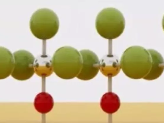
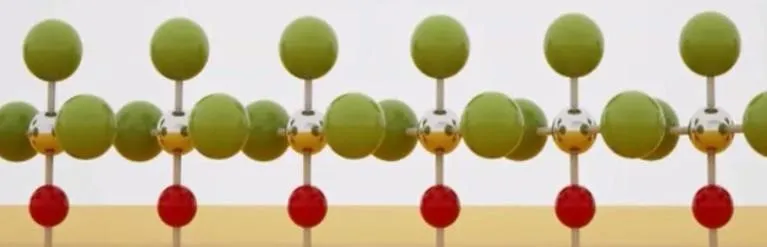
SEMI spoke with Dr. Mikko Söderlund, sales director for Beneq’s semiconductor business, about trends in Atomic Layer Deposition (ALD) applications. Söderlund shared his views ahead of his presentation at SEMI MEMS Imaging Sensors Summit, 25-27 September, 2019, at the WTC in Grenoble, France. Join us at the event to meet Beneq and other key industry influencers. Registration is open.SEMI: The Backside Illuminated (BSI) CMOS Image Sensors (CIS) market continues to experience steady growth. Which applications are currently driving market growth?Söderlund: BSI CMOS Image Sensor market continues to be driven by mobile, security, automotive and Internet of Things (IoT) applications – so there seems to be plenty of opportunities for BSI CIS market to grow further.SEMI: What is critical for advanced thin-film deposition methods to extract best electrical performance?Söderlund: It is critical to control the material properties of the deposited layer (such as charge density, resistivity or barrier property) and of course, film uniformity and conformality. Furthermore, controlling material interfaces is also important, especially for sensitive III-V materials. {% video_player "embed_player" overrideable=False, type='scriptV4', hide_playlist=True, viral_sharing=False, embed_button=False, width='350', height='197', player_id='12721134435', style='margin: 0px auto; display: block; float: right; margin-left: auto; margin-right: auto; width: 350px;' %} Coatings and material features based on existing standard techniques can be very expensive, or not feasible at all. What does Atomic Layer Deposition (ALD), as a thin film coating method, offer in particular?Söderlund: ALD offers dense, highly conformal and pinhole-free best-in-class functional layers for dielectrics, passivation, encapsulation and much more. As a gentle and precise layer-by-layer method, ALD is extremely well-suited for deposition of such performance critical layers over large surface areas such as a cassette of wafers.SEMI: Please describe the Atomic Layer Deposition (ALD) coating process. Söderlund: ALD is based on a self-limiting surface reaction controlled thin film deposition. During coating, two or more chemical vapors or gaseous precursors react sequentially on the substrate surface, producing a solid thin film (see schematic below). Most ALD coating systems use a flow-through traveling wave setup, where an inert carrier gas flows through the system and precursors are injected as very short pulses into this carrier flow. The carrier gas flow takes the precursor pulses as sequential waves through the reaction chamber, followed by a pumping line, filtering systems and, eventually, a vacuum pump.SEMI: What are the two leading edge ALD applications?Söderlund: Today’s leading-edge ALD applications are in logic (high-k/metal gate, multiple patterning) and memory (DRAM capacitor, 3D NAND). Within the More-than-Moore (MtM) markets, CIS and MEMS (actuators and sensors, RF) have been early adopters of ALD, and we also see ALD being introduced in GaN Power and RF, as well as photonics.SEMI: Give us one prediction about the opportunities offered by advanced imaging applications.Söderlund: The large diversity of imaging applications will continue to drive growth and innovation. For example, machine vision is expected to transform the imaging landscape. We see this as a big opportunity for advanced thin-film deposition methods such as ALD, provided that the tools are versatile enough to address the diverse manufacturing requirements.SEMI: What are your expectations for SEMI MEMS Imaging Sensors Summit and why do you invite your peers to attend? Söderlund: The summit brings together all key RF stakeholders in the MEMS and imaging sensors industry, and we are looking forward to a great event. It’s a special event for us as we are officially launching a new ALD cluster tool product specifically engineered for the MtM applications – so this brings great excitement that we want to share with the attendees.Dr. Mikko Söderlund is Sales Director for Beneq’s semiconductor business. He has more than 20 years of experience in product development, product management, technical sales and business development across the photonics, OLED, and semiconductor industries. Mikko received his Ph.D. in Micro- and Nanotechnology from the Helsinki University of Technology. Serena Brischetto is a marketing and communications manager at SEMI Europe.
Read More
This year, SEMI ISS covered it all – from a high-level semiconductor market and global geopolitical overview down to the neuro morphic and quantum level. Here are key takeaways from the Day 1 keynote and Economic Trends and Market Perspectives presentations.In the opening keynote, Anne Kelleher from Intel pointed to the huge growth of data, with fabs collecting more than 5 billion sensor data points each day. The challenge, Kelleher noted, is to turn massive amounts of data into valuable information. Moore’s law is not dead. New models of computing benefit still from Moore’s law and advances in Si/CMOS technologies for conventional, deep learning, neuro morphic and quantum computing.With customers expecting continual improvements in applications, the question is whether the chip industry is moving fast enough to meet these expectations, Kelleher said. A broad supply chain, equipment and materials innovations, and attracting the “best of the best” college graduates to fuel innovation is key, she said.In the economic trends session, Nicholas Burns (ambassador ret.) from Harvard University pointed out that we will see a major shift in power. The U.S. will remain the major world power over the next 10 years, but we will see a major shift in power in the next coming decades as the gap with countries like China, Russia and India continues to narrow.Duncan Meldrum from Hilltop Economics said that we are passing the peak growth of economic cycle. He warns that a more likely outlook is that a global growth recession is developing. Although semiconductor MSI growth will see a noticeable slowdown in 2019 and 2020, the semiconductor industry is still healthy over the longer term.Bob Johnson from Gartner sees demand shifting from consumer to commercial applications with higher ROIs and budgets. AI, IoT and 5D are the major enablers. He sees structural changes in the semiconductor industry especially for memory but also for Moore’s law with increasing costs and fewer players.The DRAM markets shows volatility and NAND market may be negative in 2019 but non-memory are expected to accelerate mainly because of increasing content and some price hikes.Overall Gartner expects good long-term growth with a CAGR (2017 to 2022) of 5.1%, outpacing 2011 to 2016 CAGR of 2.6%. After a strong 2018 with 13.4% revenue, he forecasts a slower 2019 with 2.6% growth followed by a 8% growth in 2020 and negative growth rate in 2021.Andrea Lati of VLSI went “Back to fundamentals” in his presentation about the industry. VLSI sees a downside bias due to slowing global economy, tariffs, and trade wars. Future drivers are data economy, cloud, AI and automotive.As memory leads the 2019 slowdown, analog, power, logic and other sectors remain in positive territory. VLSI lowered its semiconductor equipment forecast for 2018 from 20% (Jan. 2018) to 14% (Dec. 2018) but increased its sales outlook from 8% to 15% in 2018. VLSI expects revenue to slow into the first half of 2019 but increase to over 4% in the second half of the year, resulting in total 2019 drop of 2.7%. Semiconductor equipment sales are expected to drop from 14% in 2018 to -10% in 2019.Michael Corbett of Linz Consulting, covering wafer fab materials in the years of 3D scaling, sees these as good times for the industry. His outlook for wafer fab materials is bullish based on strong MSI and because wafer fab materials suppliers are getting bigger because of M As.In the Market Perspective session, Sujeet Chand of Rockwell Automation pointed out that as more and more data is generated, the problem is how to get value of all the data collected. There is a need to create the right architecture for machine learning and AI and big data is increasingly being replaced by contextual/structured data. He expects Industry 4.0 to drive foundries to become smaller, more flexible and more productive.In the Technology and Manufacturing session, Aki Sekiguchi of TEL addressed process challenges in the age of co-optimization. The semiconductor industry continues to expand, driven by massive growth of interconnected devices, with heavy demand for processing power and storage. He expects an exponential increase of data from about 40ZB in 2018 to 50ZB in 2020 to 163 ZB in 2026.Major technologies such as DRAM, 3D NAND and logic are dealing with scaling challenges. The density of DRAM (Mb/chip) is plateauing according to 2015 to 2020 trend data, with DRAM is in need of EUV. Memory capacity demand is leading to increasing layers and higher aspect ratios that is concern for 3D NAND and mainly for plasma etch. With Logic already implementing 3D structures, it appears to be in a solid position. Buddy Nicoson of Micron talked about his 50 years in the industry and looked ahead to the next 50. The anchors – quality, cost, scale and speed – won’t change. It has been a great journey so far with unprecedented opportunities and challenges ahead of us. We are getting into a convergence (specialization, integration) and solution-based phase. We will see some inflection points in the coming years, with the best yet to come.Christian G. Dieseldorff is senior principal analyst in the Industry Research and Analysis group at SEMI in Milpitas, California.
Read More
Part 1 of this article discussed the Memory Inventory Cycle Index and compared it with memory device sales and memory fab equipment investments. This article, the second of the two-part series, illustrates how the Memory Inventory Cycle Index starts to weaken before memory sales of the top three memory suppliers decline. It also shows how the Memory Inventory Cycle Index peaked in the fourth quarter of last year along with YoY growth rates for both memory sales and memory fab equipment investments.In addition to the weakening signaled by the Memory Inventory Cycle Index, memory suppliers are facing headwinds in the form of tariffs as mentioned in Micron’s most recent earnings call. The U.S.-China trade dispute could reduce Micron’s profitability; China granted a preliminary injunction to prevent Micron’s Chinese subsidiary from manufacturing and selling in China this July. However, it is very difficult to quantify the risk the tariffs pose to the future of the memory market.On the other hand, the YoY growth rate of semiconductor sales according to the World Semiconductor Trade Statistics is closely tied to China’s manufacturing sector as shown by the Purchasing Managers Index (PMI) New export orders and Orders in hand sub-indexes. Figure 3 shows that as the growth rate of new exports and order backlog slows, the YoY growth rate of semiconductor sales will be adversely impacted. As the largest consumer of semiconductors in the world, China will bear the brunt of the slowing market. Figure 3. Memory Inventory Cycle Index China manufacturing sector PMI’s sub-indices * RemarksChina PMI’s sub-indices are on the basis of the data published by NBS (National Bureau of Satistics of China). Also those data were calculated based on 12MMA (12-month moving average) to minimize seasonal fluctuation. The YoY growth rate of the 3-month moving average of semiconductor sales in China alone, China and Asia Pacific, and all regions showed additional declines in July (Figure 4). Monitoring the Orders in hand and New export orders sub-indices for China and China’s semiconductor consumption and WSTS sales revenue in China can help track the risk of trade disputes. Figure 4. YoY growth rate of semiconductor sales revenue in China and Asia Pacific * Remarks1) Regions as defined by WSTS’ Bluebook.2) Sales revenue were calculated based on 3MMA (3-month moving average value). A review of the relationship between the Memory Inventory Cycle Index, semiconductor sales, and memory fab equipment investment growth rates suggests we have passed the peak in the current cycle. However, bear in mind that the Work In Process (WIP) to Finished-goods inventory ratio has sharply increased since 2017 as shown in Figure 5. The increase in WIP inventory could be attributed to the increasing technical challenges associated with 3D NAND stacking and DRAM scaling. As a result, the proportion of finished-goods inventory in total inventory remained low until the second quarter of 2018, possibly implying that memory demand remained healthy in spite of the contraction modeled by the Memory Inventory Cycle Index. Figure 5. The proportion of finished-goods inventory in the total inventories * Remarks 1) All inventories data from 3 companies’ financial reports were calculated based on 4-quarter moving average.2) Total Inventory accounts for the sum of Finished-Goods, WIP, and Raw materials inventory.3) Company data complied by SEMI. The Memory Inventory Cycle Index has entered a period of contraction, which is supported by Micron’s weak guidance for its fiscal first quarter of 2019 (September to November). The outlook for memory sales and memory fab equipment investments reported by WSTS and SEMI, respectively, also suggests that a market correction is underway. While the low proportion of finished-goods inventory does not threaten the market yet, it should remind industry observers to view high WIP inventories with caution. Unlike past inventory cycles, the high inventory levels could burden the memory market in the absence of sustainable demand.Sungho Yoon is a senior market research analyst in Industry Research and Statistics at SEMI. SEMI China IC Ecosystem ReportLearn more about 30 new fab construction projects underway or planned in China in the newly released SEMI China IC Ecosystem Report. The research report is a comprehensive update and analysis of China's IC manufacturing ecosystem with charts, graphs, tables and maps.
Read More
On June 1st, 2018, Toshiba sold Toshiba Memory, Toshiba’s memory business, to an investment group led by Bain Capital. Toshiba Memory was then owned by a consortium of American, Japanese and Korean companies.After the long and tough negotiations, Toshiba Memory moved forward at full throttle, holding a groundbreaking ceremony for its new 3D NAND fab (100,000 WPM) in Kitakami in July and, in September, celebrating the opening of Fab 6 Phase 1 (50,000 WPM). To be sure, NAND memory is a key feature of Japan’s semiconductor industry. But the sector’s reach extends well beyond memory with its rich and versatile product portfolio nourished by active investment.Born in the early 1950s, Japan’s semiconductor industry today boasts more than 30 companies with fabs. Many feature 200mm and smaller wafer lines with legacy technologies, form factors that account for the bulk of the world’s semiconductors and are the oxygen of Japan’s chip industry. Clearly, the world is not built only with the state-of-art 7nm processed chips on the latest generation 300mm lines. Japanese chipmakers are flourishing.Automotive SemiconductorsRenesas Electronics remains a giant in microcontrollers (MCU) and system on chip (SoC) devices for automotive applications. According to IHS Markit, Renesas automotive semiconductor revenue in 2017 reached $3.6 billion while Inineon Technologies and NXP Semiconductors revenues were $3.4 billion and $3.7 billion, respectively. The three companies dominate the global automotive MCU global market. The company recently acquired Integrated Device Technology (IDT), a U.S. fabless company specializing in analog/mixed signal chips, to strengthen its automotive semiconductor portfolio. Renesas operates four volume production fabs, according to the latest World Fab Forecast from SEMI. Renesas’s microcontrollers for automotive applications (Source: Renesas Electronics) Power SemiconductorsWith power semiconductors the chips of choice for boosting the efficiency and performance of motors and batteries used in equipment, demand for the devices is rapidly growing, especially for automotive applications. Power semiconductor companies in Japan are legion and include Denso, Fuji Electric, Fujitsu Semiconductor, Hitachi, Kyocera, Mitsubishi Electric, New Japan Radio, Origin Electric, Phenitec Semiconductor, Renesas, Rohm, Sanken Electric, Sansha Electric Manufacturing, Seiko NPC, Shindengen Electric Manufacturing, Sumitomo Electric Device Innovations, Toshiba and Toyota Industries. The companies account for 26% of global power semiconductor capacity and will spend $317 million for construction and equipping in 2018.CMOS SensorsSony dominates the CMOS image sensors market with 42% share in 2016, according to Yole Développment. To meet growing demand for high-end CMOS image sensors, Sony has acquired several legacy 300mm wafer fabs and retooled them for CMOS sensor manufacturing. What’s more, Sony’s May announcement of its mid-term corporate strategy includes a 1 trillion Japanese yen investment in CMOS image sensors targeted to automotive applications by March 2021.Sony’s 7.42 effective megapixel stacked CMOS image sensor for automotive cameras (Source: Sony Corporation) MEMSMEMS is perhaps the most wide-ranging device market: Every application requires different capabilities and functions. The latest World Fab Forecast report lists 17 MEMS companies in Japan, though three makers of fast-growing RF MEMS, typically known as surface acoustic wave (SAW) or bulk acoustic wave (BAW) filters, are coming to the attention of semiconductor manufacturers. All are familiar passive electronic components suppliers – Murata Manufacturing, Taiyo Yuden and TDK – and all acquired legacy semiconductor fabs to manufacture RF MEMS.Their high-performance radio wave filters make mobile phones usable around the world. Research companies like Yole expect the introduction of 5G cellular mobile communication systems to fuel another wave of growth of the RF MEMS market. Murata Manufacturing’s SAW filters for smart phones (source Murata Manufacturing) Japanese Supply Chain Meets All Different NeedsJapan’s semiconductor supply chain provides one third of the world’s semiconductor manufacturing equipment and more than half of the industry’s materials. But Japanese suppliers also work with small and midsize makers of highly versatile chips critical to enabling the explosion of smart applications.Meet these versatile Japanese suppliers at SEMICON Japan to find solutions to your unique needs and help the world get smarter. Themed “Dreams Start Here,” SEMICON Japan 2018 reflects the promise of AI (artificial intelligence), Internet of Things (IoT) and Smart technologies. Featuring more than 750 exhibitors from around the world, the event is the gathering place to connect the people, technologies and business across the electronics manufacturing supply chain, from semiconductor manufacturing to autonomous cars, robotics and other smart applications. For more information about SEMICON Japan, visit www.semiconjapan.org.Yoichiro Ando is a marketing director at SEMI Japan.
Read More
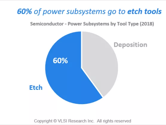
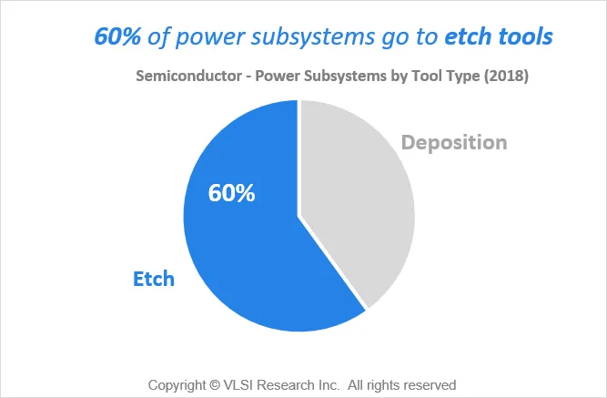
Process power and reactive gas subsystems for semiconductor manufacturing equipment have grown at a CAGR of 21% since 2013. The segment growth is considerably above the critical subsystems industry average of 9.5% and is attributable to higher demand for vacuum processing equipment over the period.Process power and reactive gas subsystems now account for approximately 12% of all expenditures on critical subsystems used on semiconductor manufacturing equipment, up from 7% in 2013. The main driver of this exceptional growth has been the rise in vacuum processing steps (deposition and etch) during the manufacturing processes of both logic and memory devices. Most deposition and etch processes require an RF generator to provide a plasma energy source in the chamber, increasing demand for tools with power subsystems such as RF power supplies and matching networks.Multiple patterning and the advent of 3D NAND in high-volume manufacturing have significantly increased the number of deposition and etch processing steps and, in the case of 3D NAND, longer and more difficult etch processes are requiring a wider range of power solutions. Further analysis shows that 3D NAND has been the principle growth catalyst, with the total share of power subsystems going to memory applications increasing 8 percentage points since 2013. Memory applications now account for almost half of all power subsystems demand in 2018. Interestingly, investigation of power subsystems by tool type reveals that a clear majority of power subsystems (60%) find their way on to etch tools with only 40% on deposition tools. This can be explained by the fact that more delicate etch processes can require multiple RF power solutions per tool, whereas deposition does always use plasma energy sources, for example in thermal deposition processes.Despite the staggering growth performance of the power subsystems segment over the past five years, we expect the growth rate to moderate significantly in the run-up to 2023. Now that 3D NAND has been adopted in high-volume manufacturing, we expect the rate of increase in vacuum/plasma processing steps to slow down. The introduction of EUV also has the potential to taper demand for vacuum processing equipment. However, it is not expected the reverse the trend as multiple patterning techniques will still be needed in conjunction with EUV to achieve the desired improvements in device density and performance. The future growth trend for power and reactive gas subsystems is forecast to be in line with the critical subsystems industry average at approximately 2.0% CAGR until 2023.For more information about Critical Subsystems and VLSI Research, please visit www.vlsiresearch.com/public/csubsJulian West is a technical and market analyst at VLSI Research Europe.
Read More
Korea is on track to top all other regions in fab investment, spending $63 billion between 2017 and 2020, with powerhouses Samsung Electronics Co. and SK Hynix leading the way, according to latest World Fab Forecast Report by SEMI. Samsung Electronics increased fab investments $770 million to $12 billion this year, and SK Hynix upped its spending a significant $2.8 billion to $7.25 billion in 2018.Korea's investment companies anticipate continued growth for both companies in the second half of 2018.Under this halo of extraordinary investment, nearly 380 SEMI Korea members and industry analysts gathered for 2018 SEMI Korea Members Day on September 13 to share insights on semiconductor market trends and new technologies that could help members bolster their competitiveness. Following are key takeaways from the event. Korea semiconductor market to grow 16% in 2018That’s according to IDC Korea VP Kim Soo-kyung, who noted that data center, memory and Internet of Things (IoT) are becoming key growth drivers for the semiconductor industry. He encouraged semiconductor companies to closely track development of automotive technology and the industry semiconductor market, both key growth areas. SEMI Korea president H.D. Cho opens SEMI Korea Members Day 2018 Continuing fab investment will lead to oversupply, but display will shineMarket entry by Chinese companies will also spur the oversupply, said Jeong Won-Seok, an analyst at HI Investment Corp. He noted that the oversupply will force Korea into stiffer competition with other regions. However, with OLED used for a wide variety of devices and the display industry seeing rapid growth, the sector will remain ripe for growth among Korean companies.Interconnecting various applications is a big semiconductor industry trendThe need for these interconnections will stand out in the mobility and high-performance computing (HPC) markets, said Park Sung-Soon, principal research fellow at Amkor Technology Korea, who addressed trends in packaging technology. He also emphasized interconnection cost efficiency as key to maximizing competitiveness.Smart Manufacturing is driving mass customizationAs semiconductor industry growth continues, production methods are shifting from ‘mass production’ to ‘mass customization,’ increasing the importance of Smart Manufacturing in driving greater production efficiency, noted BISTel VP Jeon Kyeong-Sik. Building a Smart Manufacturing platform to support large-scale production of specialized database and artificial intelligence (AI) chips will boost production efficiency, reduce costs and improve risk management. Virtual simulation will be a key enabling technology. SEMI analyst Clark Tseng presenting at SEMI Korea Members Day 2018 Surge in data volume and technology advances to drive long-term semiconductor industry growthThese key industry drivers will continue to power fab investment growth, with spending focused on 3D NAND, DRAM, and foundry, said Clark Tseng, director of Industry Research and Statistics at SEMI. China alone will see eye-watering growth with the region’s investments in domestic companies surging 46% from 2018 to 2019 and fab investment by Chinese domestic companies outpacing spending by foreign companies in China, Tseng predicted. SEMI membership rises with industry growthCulminating the event, SEMI Korea president H.D. Cho said, "With the growth of the semiconductor market, the number of SEMI members is gradually increasing, and we will help member companies grow with various activities such as Korea Members Day.”Jaegwan Shim is a marketing specialist at SEMI Korea.
Read More
SEMI Releases latest update to World Fab Forecast with adjusted semiconductor revenue consensus for second-half 2018 and 2019 Global semiconductor revenue in 2018 is now expected to reach $473.8 billion and clock a growth rate of 15 percent, a significant upward revision from the 7.5 percent expansion (to $442.9 billion) forecast at the start of the year by six research and investment forecasts tracked by SEMI Industry Research and Statistics (SEMI IR S). Data center growth will remain robust in the coming quarters, fueling demand for memory devices. In addition, cloud computing will continue to spur strong CPU, GPU, networking, ASIC, and DRAM and NAND demand through 2019, driving a consensus 3.63 percent year-to-year growth to reach the semiconductor revenue of $491 billion in 2019. Fab equipment spending (new and used) for 2018 is expected to increase by 14 percent to a record high of $63 billion, according to the last data from the SEMI World Fab Forecast, published by SEMI IR S. For 2019, fab equipment spending (new and used) is expected to increase 8 percent to another record of just under $68 billion. Memory continues to be the biggest swing factor in fab spending in 2018 and is expected to lead growth into 2020. 3D NAND will see the most capacity added in 2018 and 2019 with growth of 41 percent in 2018 and 27 percent in 2019, according to the SEMI World Fab Forecast. DRAM investment will see even stronger growth in 2018 and 2019 driven by new capacity addition as well as the continued technology shrink towards 1y/1z nm. For the first half of 2018, global spending for semiconductor fab equipment continues its growth momentum from 2017. Though we expect some softness in the second half of 2018, the outlook for 2019 remains robust with a fourth consecutive year of growth – the first such run since the 1990s. This prolonged growth cycle has been propelled by memory and will be extended by significant investment in China in 2019. Although a potential slowdown in 2020 is a concern, the overall outlook for semiconductor demand remains solid due to broad-based growth trends in data center, artificial intelligence (AI)/machine learning (ML), automotive, and industrial segments. Following are other SEMI forecasts for fab spending. Installed Capacity 3D NAND will see the most capacity added in both 2018 and 2019 with growth of 41 percent in 2018 and 27 percent in 2019. Foundry capacity growth is steady at 3 percent in 2018 and 6 percent in 2019, driven by both leading-edge and trailing-edge capacity buildup. 200mm fab capacity will increase 4 percent in 2018 and 3 percent in 2019, fueled by demand for MCU, sensors, PMIC, MOSFET and Driver IC. New Facilities / Construction Spending In 2018, there are 72 construction projects with investments totaling $15 billion, a year-over-year increase of 23 percent. Construction spending will reach all-time highs with China continuing its lead at US$7 billion in 2018, shattering its own record of $6.3 billion investment in 2017. Most construction spending in 2018 will be for Memory (just under $9 billion), primarily for 3D NAND followed by DRAM. Foundry will log second place in construction spending at just under $5 billion. Fab Equipment Spending Fab equipment spending (new and used) for 2018 is expected to jump 14 percent to a record high of US$63 billion, flat from the forecast issued in June 2018. Equipment spending (new and used) for 2019 is expected to increase 8 percent to another record of just under US$68 billion, a downward adjustment from +9 percent published in June 2018. We believe equipment spending will remain healthy, driven by solid, broad-based demand and predictable technology investments on top of constructive SEMICAP equipment fundamentals. Activity Report The August report features 1,265 records including about 300 Opto- and LED-related facilities. We have made 223 changes related to 216 fabs/lines. The modifications include the addition of new records, changes to existing records, the deletion of records since the February 2018 World Fab Forecast report. We are tracking 103 future facilities/lines with various probabilities that will start volume production in 2018 or later. Download a sample report Not a subscriber? Please review SEMI fab databases listed below. Our databases deliver the latest forecast and a complete analysis of front-end fabs and foundries worldwide. They are ideal resources to empower your market research. Eugenia Liu is a Senior Product Marketing Manager at SEMI.
Read More
What’s next for smarter, more connected electronics manufacturing - Part 2The fast-maturing infrastructure now enabling applications for big data and artificial intelligence means disruptive change not just at individual companies but also in data connections among companies across the microelectronics manufacturing value chain. SEMI checked in with some leading players on the changes they see coming in the next several years for this article series. The trade group is expanding its programming on smart manufacturing to address these industry-wide developments at SEMICON West, July 10-12 in San Francisco.“The ramp of EUV, and the smaller geometries and smaller process margins, will drive an exponential increase in the amount of metrology data to manage,” says Neal Callan, ASML vice president, Silicon Valley. Callan notes that moving to multibeam e-beam inspection will increase data volume from megabytes per second to gigabytes per second and from thousands of data points to millions of data points. “The process is so tight and the margin so small that stochastic variation, or noise, becomes more dominant – at least it’s noise until we can learn to understand and control it. And understanding and controlling this variation will be key to delivering 5nm patterning,” he says.Single-beam e-beam inspection is already driving large increases in data as engineers extend the slow technology to broad, high-speed defect metrology applications by more intelligently instructing the system where to look for problems. Callan says ASML is now using the scanner data on wafer focus, alignment and leveling. The company is also using the computational lithography model from the design to identify the smallest process windows in the pattern that are most likely to see problems. The model then quantifies the number and significance of those instances.“The collection of all this diverse data means that tools will need to be plug-and-play so all tool data is instantly available to all systems and software,” says Doug Suerich, PEER Group product evangelist. “We need tools that can be discovered automatically by the network so it can start slurping up data immediately. The adoption of the Interface A (EDA) standard is accelerating and fabs are starting to ask for it. The proliferation of sensors also needs to self-discover. If you are going to add thousands of new sensors into a facility, you can’t afford a time-consuming integration process.”“We are now seeing that engineers are greedy for more data – if they can get the data, it’s becoming a need-to-have,” adds Tom Ho, BISTel America president. “Getting more data from more sensors, from the sensors on the tool that are not being fully utilized, and from untapped data sources like vibration is another big coming opportunity.” Process complexity drives demand for feed-forward between silos with computational models ASML co-optimizes its scanner process with etch and reticle process steps. Source: ASML In addition to the drive for trace-back of data, the increasing complexity of interrelated processes is also driving demand for feed-forward of data. “Feed-forward is becoming more important,” notes Ho. He points to the example of 3D NAND features, now getting so deep that identifying the layer being measured is a challenge unless the signal at the step before can be recognized. “We need partnerships with our peers to understand how to take advantage of the sensors they use, integrate them with our data, and then feed-forward corrections to the other systems,” concurs Callan. “To drive the best CD uniformity and overlay, we need to co-optimize litho and etch,” agrees Henk Niesing, ASML director of product management. He notes that the company is working with etcher makers to measure the overlay and CD, decompose the finger prints, and then use models to steer automated control that best adjusts both the scanner and the etcher. ASML is also working with Zeiss on co-optimization between the scanner and the reticle to make even higher-order corrections by locally modifying the reticle.These higher-order corrections, applied on each exposed field, drive the need for even more data, and at higher speed but without higher cost, notes Jan Mulkens, ASML senior fellow. These corrections increase demand for computational metrology, which combines various metrology sources with physics and deep learning models trained on real data to predict and control process results in real time. “We’re working on computational metrology to ideally use all the knobs we have in the fab,” he says. So far this effort has largely involved linking data between two companies. More consistent data formats would enable data exchange to be extended to more companies. “The software versions also need to be managed for upgrades so they still match after one party updates the system on its tool,” notes Niesing. Speakers on these issues of smart manufacturing and data handling at SEMICON West include Active Layer Parametrics, Applied Materials, Applied Research Photonics, ASML, Cimetrix, Coventor, ECI Technologies, Edwards Vacuum, Final Phase Systems, GE Digital, Infineon, Jabil, Lam Research, Osaro, Otosense, PEER Group, Rockwell Automation, Rudolph Technologies, Schneider Electric, Seagate, Seimens, Stanford University, TEL, TIBCO Software. See semiconwest.org.What’s next for smarter, more connected electronics manufacturing - Part 1What’s next for smarter, more connected electronics manufacturing - Part 3Paul Doe, SEMI
Read More