downloadGroupGroupnoun_press release_995423_000000 copyGroupnoun_Feed_96767_000000Group 19noun_pictures_1817522_000000Member company iconResource item iconStore item iconGroup 19Group 19noun_Photo_2085192_000000 Copynoun_presentation_2096081_000000Group 19Group Copy 7noun_webinar_692730_000000Path
Skip to main content
Default Banner Image

Automotive

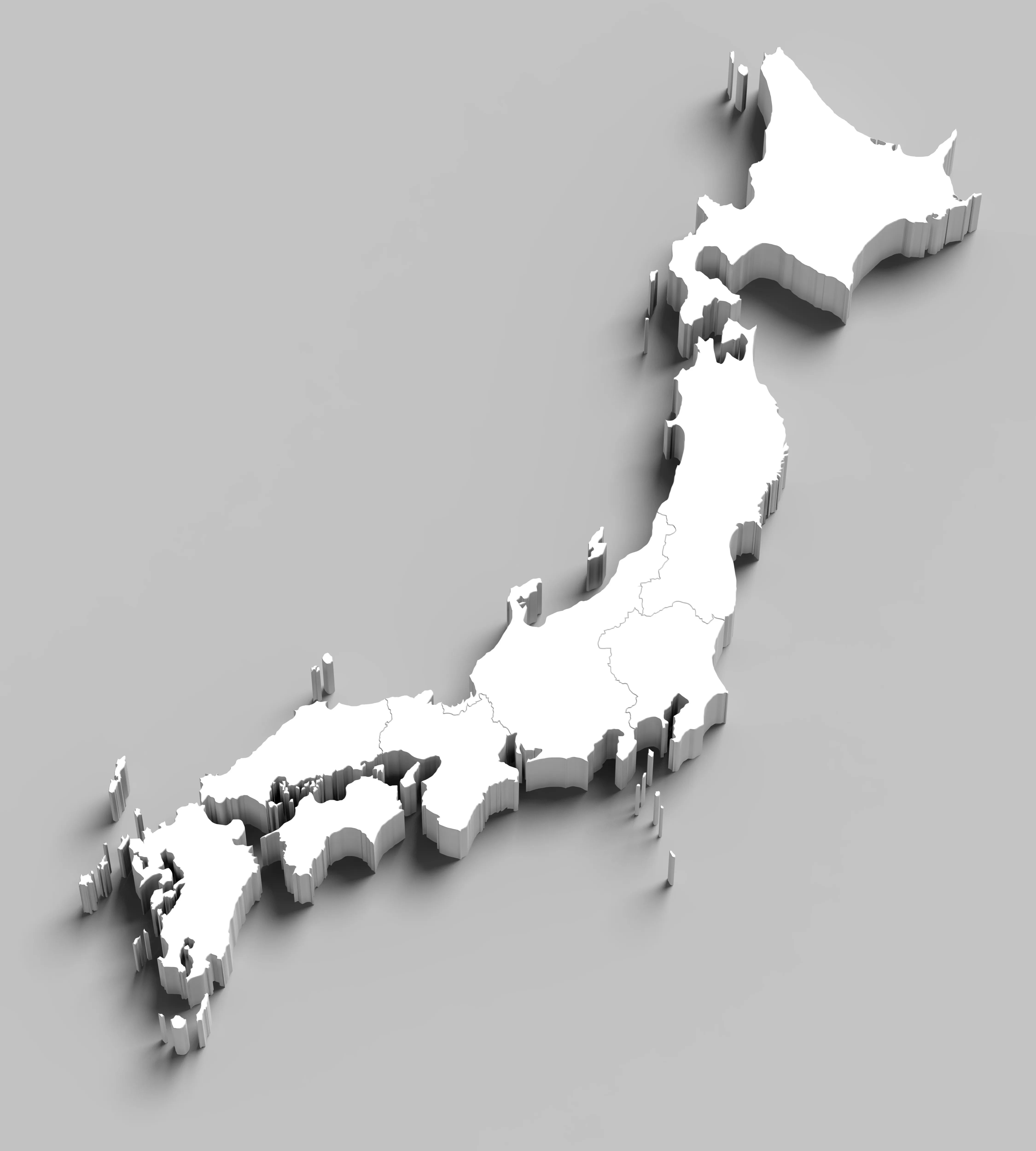
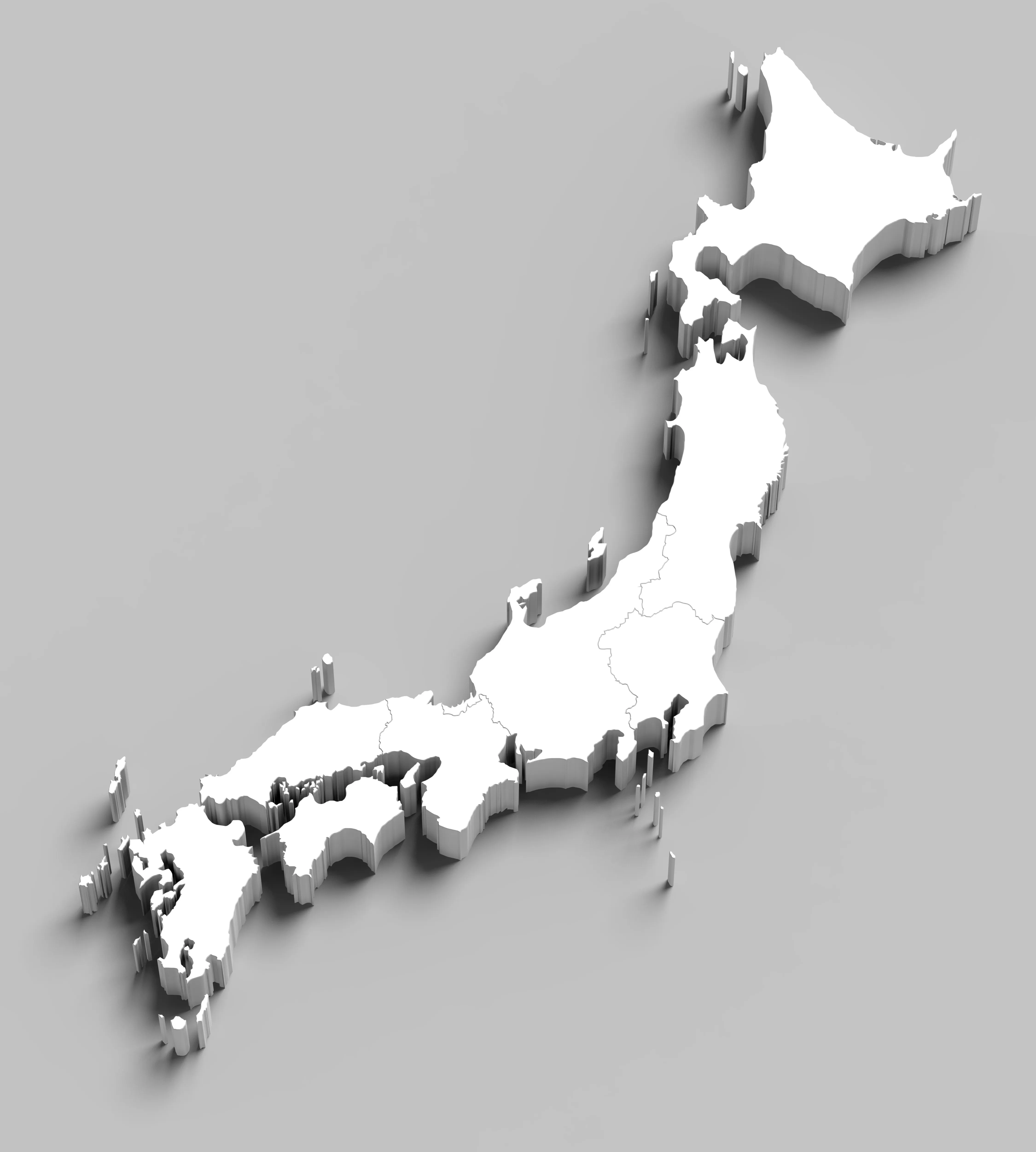
Kyushu, the third largest island in Japan, is home to the semiconductor production bases of integrated device manufacturers (IDMs) with world-class cutting-edge technology. SONY, Toshiba, Hitachi, Mitsubishi, Fujitsu and Nissan are among the sector’s shining stars, though a host of other IDMs tied to the supply chains of other major enterprises have also set root in Kyushu. Collectively, the companies earned Kyushu the name Silicon Island of Japan.Kyushu’s flourishing IDM industry sprouted from favorable tax and other government policies that reduced semiconductor production costs to levels lower than elsewhere in Japan. Once the IC producers had established bases, equipment and materials companies naturally followed, leading to the influx of many parts manufacturers. Together, they came to Kyushu, one after another, to make the island a magnet for manufacturing. And so it was to Kyushu that a SEMI China delegation travelled for a meeting at TEL’s factory in Kumamoto to learn more about the secrets to the rapid growth of the island’s semiconductor industry and promote cooperation between Chinese and Japanese enterprises. Underscoring the rise of the Silicon Island of Japan, China will soon become TEL’s largest market, said Masami Akimoto, Chairman of Tokyo Electron Kyushu Limited, speaking at the event. Masami Akimoto hopes for support from SEMI China.The island of 12 million people contributes to the growth of the global semiconductor industry, expected to reach USD 500 billion in size in 2019 as China’s semiconductor sector, fueled in part by government-backed investment funds, continues its rapid expansion. Despite the gains, China still lags other regions in advanced manufacturing, said Lung Chu, president of SEMI China, which is doing its part to draw more advanced manufacturing to the region through its SIIP platform. The initiative encourages pan-regional cooperation with China’s semiconductor industry to promote free trade, open markets, technology innovation and IP protection – all to help China better integrate with the global semiconductor industry. SEMI China President Lung Chu(L) issues visit memorial to Masami Akimoto(R), Chairman of Tokyo Electron Kyushu Limited. Chicken shall be led by the HenUnlike other regions with comprehensive semiconductor industries, Kyushu’s is primarily focused on production and assembly, with more than 200 manufacturers of semiconductor equipment and parts.SEMI China Delegation at Tokyo Electron Kyushu LimitedTEL built its first factory in Kumamoto, a city covered by volcanic ash in the center of Kyushu, 34 years ago. Today, TEL every month produces 80 to 90 sets of equipment, each consisting of, on average, over 400 thousand parts that must be certified and authorized by TEL before delivery to its module manufacturers and assembly into complete machines. Having blossomed over the past few decades, the island’s supply chain now supplies TEL with all its equipment parts. SEMI China Delegation at Fajita WorksTEL supplier Fajita Works, a high-precision plate metal manufacturer founded in 1945, is emblematic of other companies in the Kyushu supply chain. It keeps a low public profile as it serves several longtime customers and earns ardent loyalty from its workers, an ethos reflected in the change next January of its slog from “Only One” to “Great company, Great life.”Quality is the life of the enterpriseLong before the rise of its legendary automobile and consumer electronics companies, Japan was known for inferior, counterfeited products, labeled “Made In USA” and shipped to the United States by more than 100 factories. The net effect was to shrink and commoditize American markets. The tide in Japan’s product quality and stained reputation began to turn in the 1980s, when Japan’s semiconductor industry began to produce memory with an error rate 27 times lower than its U.S. competitors, giving Japan an upper hand in quality that it would never relinquish. SEMI China Delegation at HORIBAKyushu-based flowmeter supplier HORIBA, among the many Japanese companies famous for their product quality, ships 38 percent of its products into the automotive market and 27 percent into the semiconductor sector. Cleanliness is as vital a part of the company’s culture as quality. Each depends on the other, with fine detail held to the highest importance. On its visit to HORIBA, the SEMI China delegation, passing by an office area before entering the factory, sighed at the sight of the spotless, neatly kept furniture and workspace: They had never seen an office so sparkling clean. HORIBA’s success is rooted in immaculate offices, factories and the company’s motto “Enjoy innovation and pay close attention to product quality.”After Kumamoto sustained heavy damage during a 2016 earthquake, HORIBA workers returned rocks scattered by temblor to their original position, knowing that order is critical to lean, efficient manufacturing and that, indeed, “the devil is in the details.” SEMI China Delegation in Kumamoto City Full confidence in the exploration of Chinese marketConsumer electronics stalwarts Sony and Panasonic feature semiconductor factories in Kagoshima, the southernmost city in Kyushu and Japan, though rumor had it two years ago that Panasonic planned to pull out. The Panasonic plant, which provides batteries for Tesla, remains. The Sony facility produces image sensors for the iPhone.Semiconductor equipment maker ULVAC, SEMI China’s most important strategic partner, is also based in Kagoshima. During the delegation’s visit to the company, Lung Chu noted that while China is the world’s largest semiconductor market, the region meets just 13 percent of domestic chip demand. Stressing that ULVAC can play a crucial role in helping China become a bigger player, he expressed admiration for ULVAC’s professionalism along with hope that it will maintain its rapid growth and leverage SEMI resources to catalyze rapid development of Internet of Things (IoT), artificial intelligence (AI), and 5G technologies in China and rise into the top 10 of global equipment manufacturers. SEMI China President Lung Chu (L) issues visit memorial to ULVAC Kyushu President and CEO Kenji Yamaguchi ULVAC Kyushu president and CEO Kenji Yamaguchi made clear the company’s interest in Lung Chu’s insights into Chinese semiconductor industry while underscoring its core competency of producing semiconductors for flat panel displays. The Kyushu Factory of ULVAC is full of vitality and market competitiveness. SEMI China Delegation at ULVAC EBARA, a precision machinery company located in Kumamoto, has manufactured chemical-mechanical planarization (CMP) equipment for over 20 years and delivered nearly 2,400 mechanical polishing machines worldwide. While the company expects to ship 50 sets per year to China starting next year, it has the capacity to deliver 20 sets per month, enough to meet demand of Chinese semiconductor makers. SEMI China Delegation at EBARAThe most telling takeaway from the SEMI China delegation’s visit to the Kyushu: Japan ranks number one worldwide in research and development (R D) investment as a proportion of GDP and is also at the top in the percentage of R D funds controlled by private enterprises. The outsize investment strategy has enabled Japan to maintain its hold as one of the world’s top technology innovators.Like Sakurajima, the famed Kyushu volcano, the SEMI China delegation will continue to harness its forces to build relationships with the island’s semiconductor supply chain as it works to develop win-win pan-regional relationships and foster the growth of China’s semiconductor industry. Best view of Sakurai volcano Gang Yao is a marketing director at SEMI China.
Read More
On June 1st, 2018, Toshiba sold Toshiba Memory, Toshiba’s memory business, to an investment group led by Bain Capital. Toshiba Memory was then owned by a consortium of American, Japanese and Korean companies.After the long and tough negotiations, Toshiba Memory moved forward at full throttle, holding a groundbreaking ceremony for its new 3D NAND fab (100,000 WPM) in Kitakami in July and, in September, celebrating the opening of Fab 6 Phase 1 (50,000 WPM). To be sure, NAND memory is a key feature of Japan’s semiconductor industry. But the sector’s reach extends well beyond memory with its rich and versatile product portfolio nourished by active investment.Born in the early 1950s, Japan’s semiconductor industry today boasts more than 30 companies with fabs. Many feature 200mm and smaller wafer lines with legacy technologies, form factors that account for the bulk of the world’s semiconductors and are the oxygen of Japan’s chip industry. Clearly, the world is not built only with the state-of-art 7nm processed chips on the latest generation 300mm lines. Japanese chipmakers are flourishing.Automotive SemiconductorsRenesas Electronics remains a giant in microcontrollers (MCU) and system on chip (SoC) devices for automotive applications. According to IHS Markit, Renesas automotive semiconductor revenue in 2017 reached $3.6 billion while Inineon Technologies and NXP Semiconductors revenues were $3.4 billion and $3.7 billion, respectively. The three companies dominate the global automotive MCU global market. The company recently acquired Integrated Device Technology (IDT), a U.S. fabless company specializing in analog/mixed signal chips, to strengthen its automotive semiconductor portfolio. Renesas operates four volume production fabs, according to the latest World Fab Forecast from SEMI. Renesas’s microcontrollers for automotive applications (Source: Renesas Electronics) Power SemiconductorsWith power semiconductors the chips of choice for boosting the efficiency and performance of motors and batteries used in equipment, demand for the devices is rapidly growing, especially for automotive applications. Power semiconductor companies in Japan are legion and include Denso, Fuji Electric, Fujitsu Semiconductor, Hitachi, Kyocera, Mitsubishi Electric, New Japan Radio, Origin Electric, Phenitec Semiconductor, Renesas, Rohm, Sanken Electric, Sansha Electric Manufacturing, Seiko NPC, Shindengen Electric Manufacturing, Sumitomo Electric Device Innovations, Toshiba and Toyota Industries. The companies account for 26% of global power semiconductor capacity and will spend $317 million for construction and equipping in 2018.CMOS SensorsSony dominates the CMOS image sensors market with 42% share in 2016, according to Yole Développment. To meet growing demand for high-end CMOS image sensors, Sony has acquired several legacy 300mm wafer fabs and retooled them for CMOS sensor manufacturing. What’s more, Sony’s May announcement of its mid-term corporate strategy includes a 1 trillion Japanese yen investment in CMOS image sensors targeted to automotive applications by March 2021.Sony’s 7.42 effective megapixel stacked CMOS image sensor for automotive cameras (Source: Sony Corporation) MEMSMEMS is perhaps the most wide-ranging device market: Every application requires different capabilities and functions. The latest World Fab Forecast report lists 17 MEMS companies in Japan, though three makers of fast-growing RF MEMS, typically known as surface acoustic wave (SAW) or bulk acoustic wave (BAW) filters, are coming to the attention of semiconductor manufacturers. All are familiar passive electronic components suppliers – Murata Manufacturing, Taiyo Yuden and TDK – and all acquired legacy semiconductor fabs to manufacture RF MEMS.Their high-performance radio wave filters make mobile phones usable around the world. Research companies like Yole expect the introduction of 5G cellular mobile communication systems to fuel another wave of growth of the RF MEMS market. Murata Manufacturing’s SAW filters for smart phones (source Murata Manufacturing) Japanese Supply Chain Meets All Different NeedsJapan’s semiconductor supply chain provides one third of the world’s semiconductor manufacturing equipment and more than half of the industry’s materials. But Japanese suppliers also work with small and midsize makers of highly versatile chips critical to enabling the explosion of smart applications.Meet these versatile Japanese suppliers at SEMICON Japan to find solutions to your unique needs and help the world get smarter. Themed “Dreams Start Here,” SEMICON Japan 2018 reflects the promise of AI (artificial intelligence), Internet of Things (IoT) and Smart technologies. Featuring more than 750 exhibitors from around the world, the event is the gathering place to connect the people, technologies and business across the electronics manufacturing supply chain, from semiconductor manufacturing to autonomous cars, robotics and other smart applications. For more information about SEMICON Japan, visit www.semiconjapan.org.Yoichiro Ando is a marketing director at SEMI Japan.
Read More
SEMI FabView update for calendar year Q3 2018 Global fab construction investment shows continuing strength, with 19 new fab projects expected to begin construction in 2019 and 2020, based on the latest data published in SEMI’s World Fab Forecast. Fab investment is just one indicator of how growing demand in areas such as high-performance computing, data storage, artificial intelligence (AI), cloud computing, and automotive are driving the fourth consecutive year of spending growth in the semiconductor industry. Below are a few highlights* from September’s SEMI FabView: Memory: Not fading Micron plans to invest $3 billion by 2030 in Manassas, Virginia – These investments, driven by strong demand for automotive applications, are contemplated in Micron's long-term model. The production ramp is anticipated to be in the first half of 2020. SK Hynix to build new DRAM fab in Icheon (Gyeonggi Province), Korea – The construction, to be completed by the end of 2020, will adopt 1znm node (probably EUV). Total investment is estimated to exceed $13 billion. Nanya Technology doubles 2018 capex plan – The increase is for additional DRAM capacity and more 20nm DRAM conversion (from 30nm). 200mm and below: Not leading edge, but continues to draw investment Vanguard changes fab investment strategy – Vanguard will focus on 200 mm and has scrapped its plan for 300mm expansion. Murata to invest into 150mm expansion – Murata announced a 5 billion Yen investment (US$44.6 million) in a new fab extension in Vantaa, Finland. Investment, M A in Analog, Logic, Power and Opto Segments Texas Instruments is looking to invest $3.2 billion in new fab construction in 2019 – Texas Instruments is eyeing Richardson, Texas and also considering sites outside Texas. Bosch 300mm fab in Dresden, Germany – Bosch held a groundbreaking ceremony on April 24. Equipment installation is expected in 2H19. Microchip completes acquisition of Microsemi – Microchip closed its $8.45 billion acquisition of Microsemi on May 29. Microsemi has five fabs in the U.S. with a wide range of semiconductor products and system solutions. New fabs in China keep on coming Shanghai Jita Semiconductor/Huada Semiconductor – Shanghai Jita Semiconductor, a subsidiary of Huada Semiconductor and China Electronics Corporation (CEC), announced plans earlier this month to build both 200 mm and 300 mm semiconductor fabs for analog and power semiconductors in Shanghai. The combined fab investment will total $5.18 billion. Hamamatsu Photonics building 200 mm fab – Hamamatsu announced that it is building a new facility Investment of 2.8 billion Yen (US$25 million) to boost opto semiconductor capacity. Production is anticipated to start in late 2019. * Actual FabView updates provide more detail SEMI FabView, a mobile-friendly, interactive version of SEMI’s popular World Fab Forecast, delivers on-demand fab information such as fab spending and capacity for over 1,200 facilities, including over 60 planned facilities worldwide, across a wide range of product segments including Power, GPU, Memory, Foundry, MEMS and Sensors fabs. Fab data include region, start of construction, operation, construction and equipment spending, capacity, wafer sizes, product types and geometries. SEMI FabView subscribers receive forecast model updates through SEMI’s World Fab Database. Click here for a trial if you want to experience SEMI FabView first hand. Christian G. Dieseldorff is senior principal analyst and Eugenia Liu is senior product marketing manager, Industry Research and Statistics, SEMI, Milpitas, California.
Read More
SEMI Releases latest update to World Fab Forecast with adjusted semiconductor revenue consensus for second-half 2018 and 2019 Global semiconductor revenue in 2018 is now expected to reach $473.8 billion and clock a growth rate of 15 percent, a significant upward revision from the 7.5 percent expansion (to $442.9 billion) forecast at the start of the year by six research and investment forecasts tracked by SEMI Industry Research and Statistics (SEMI IR S). Data center growth will remain robust in the coming quarters, fueling demand for memory devices. In addition, cloud computing will continue to spur strong CPU, GPU, networking, ASIC, and DRAM and NAND demand through 2019, driving a consensus 3.63 percent year-to-year growth to reach the semiconductor revenue of $491 billion in 2019. Fab equipment spending (new and used) for 2018 is expected to increase by 14 percent to a record high of $63 billion, according to the last data from the SEMI World Fab Forecast, published by SEMI IR S. For 2019, fab equipment spending (new and used) is expected to increase 8 percent to another record of just under $68 billion. Memory continues to be the biggest swing factor in fab spending in 2018 and is expected to lead growth into 2020. 3D NAND will see the most capacity added in 2018 and 2019 with growth of 41 percent in 2018 and 27 percent in 2019, according to the SEMI World Fab Forecast. DRAM investment will see even stronger growth in 2018 and 2019 driven by new capacity addition as well as the continued technology shrink towards 1y/1z nm. For the first half of 2018, global spending for semiconductor fab equipment continues its growth momentum from 2017. Though we expect some softness in the second half of 2018, the outlook for 2019 remains robust with a fourth consecutive year of growth – the first such run since the 1990s. This prolonged growth cycle has been propelled by memory and will be extended by significant investment in China in 2019. Although a potential slowdown in 2020 is a concern, the overall outlook for semiconductor demand remains solid due to broad-based growth trends in data center, artificial intelligence (AI)/machine learning (ML), automotive, and industrial segments. Following are other SEMI forecasts for fab spending. Installed Capacity 3D NAND will see the most capacity added in both 2018 and 2019 with growth of 41 percent in 2018 and 27 percent in 2019. Foundry capacity growth is steady at 3 percent in 2018 and 6 percent in 2019, driven by both leading-edge and trailing-edge capacity buildup. 200mm fab capacity will increase 4 percent in 2018 and 3 percent in 2019, fueled by demand for MCU, sensors, PMIC, MOSFET and Driver IC. New Facilities / Construction Spending In 2018, there are 72 construction projects with investments totaling $15 billion, a year-over-year increase of 23 percent. Construction spending will reach all-time highs with China continuing its lead at US$7 billion in 2018, shattering its own record of $6.3 billion investment in 2017. Most construction spending in 2018 will be for Memory (just under $9 billion), primarily for 3D NAND followed by DRAM. Foundry will log second place in construction spending at just under $5 billion. Fab Equipment Spending Fab equipment spending (new and used) for 2018 is expected to jump 14 percent to a record high of US$63 billion, flat from the forecast issued in June 2018. Equipment spending (new and used) for 2019 is expected to increase 8 percent to another record of just under US$68 billion, a downward adjustment from +9 percent published in June 2018. We believe equipment spending will remain healthy, driven by solid, broad-based demand and predictable technology investments on top of constructive SEMICAP equipment fundamentals. Activity Report The August report features 1,265 records including about 300 Opto- and LED-related facilities. We have made 223 changes related to 216 fabs/lines. The modifications include the addition of new records, changes to existing records, the deletion of records since the February 2018 World Fab Forecast report. We are tracking 103 future facilities/lines with various probabilities that will start volume production in 2018 or later. Download a sample report Not a subscriber? Please review SEMI fab databases listed below. Our databases deliver the latest forecast and a complete analysis of front-end fabs and foundries worldwide. They are ideal resources to empower your market research. Eugenia Liu is a Senior Product Marketing Manager at SEMI.
Read More
Standing-room only keynote speeches. A future awash in data amassed by transformative technologies and applications, with semiconductors at their core. Smart everything: Cars, medicine, manufacturing, workforce, you name it. The sheer numbers impressed as a record lineup of SEMICON West keynote speakers offered a glowing portrait of the future: The semiconductor industry stands on the cusp of a breakout expansion. Standing and seated shoulder-to-shoulder in the packed-to-gills opening keynote, the audience learned, indeed, that the best was yet to come: “This is the best SEMICON West, ever,” observed SEMI CEO Ajit Manocha. Here’s a glimpse of the keynotes by the numbers, starting with the luckiest of all. 7 – The number of keynotes – among the brightest lights in technology – sharing their visions of the future through the lens of breakthrough technologies that are nearly ready to make their indelible mark. Dozens of expert panelists also weighed in at SEMICON West, the annual U.S. flagship microelectronics gathering in San Francisco. 90 – The percentage of all data ever generated has been created in just the past two years as the cloud mushrooms with tweets, texts, emails, Facebook posts, YouTube videos, medical records and all manner of business information, noted Bill Bottoms, president and CEO of Third Millennium Test Solutions. In the years ahead, an almost unimaginable wealth of data will require analysis by artificial intelligence (AI) embedded in semiconductors to enable applications that go well beyond smart. 12-18 – That’s how many months it will take for data volume to double, predicted John Kelly III, IBM’s Senior VP, Cognitive Solutions. And it will double again and again, every 12-18 months. Kelly foresees a scale of growth “that will dwarf previous eras of computing … the number of opportunities is enormous.” Kelly’s four decades in computing gave considerable weight to his point that “in the industry, there has never been a more exciting point in time than today.” First – Technology is being re-born. Using baseball lingo, several speakers noted that we are just in “the first inning,” “the top half of the first inning” or “the beginning of the first inning” to make clear in the most emphatic terms the duration of prosperity that lies ahead for the industry. AI embedded in chips and demand for real-time analysis of AI data will be its fuel. As SEMI Americas president Dave Anderson observed with a smile, “We all know how long baseball games can go.” Third – That’s the current wave of machine learning the world is now experiencing, according to Sandia National Laboratories’ Principal Member Conrad James. Computers are now capable of solving many increasingly complex problems on their own, with no human intervention necessarily required, he said. 1000x – As spectacularly fast as computing power already is today, the industry will need to double that the rate of performance in the years ahead, predicted Applied Materials president and CEO Gary Dickerson. Demand for this herculean processing capacity will spur a “tremendous focus on innovation” among SEMI members, their customers and their customers’ customers. 5 to 15 – The remarkable amount of silicon that power today’s mobile devices will be overshadowed by the chips – equivalent in computing capacity to 5 to 15 cell phones – that will be the engine of self-driving and other features in future automobiles, predicted Pierre Ferragu, New Street Research Managing Partner, during the SEMI Bulls and Bears session. Automobiles with this souped-up computing capacity will sell in the millions worldwide in the years ahead, generating never-before-seen opportunities for the chip industry, he noted. 10,000 – It’s not just cars. Ten thousand is the number of sensors that will be built just into the wings of new Airbus A380-1000 aircraft, AMD CTO Mark Papermaster explained during his keynote. 10 terabits – The staggering amount of Facebook data uploaded daily in to the cloud, Papermaster noted. 1 Trillion – SEMI’s 2020 forecast that the industry will reach $500 billion in revenues by 2020 was eclipsed by one analyst, speaking at the SEMI Market Symposium on the first day of the event, predicted that the industry would top $1 trillion in the foreseeable future. SEMI’s Manocha later added that $1 trillion in industry revenue is possible by 2030, “maybe sooner.” 1 (sexy) coda – Coders are hip and software applications are the apple of the world’s eye. Even the most casual mobile device user knows that software apps makes it whirl. But “hardware is becoming sexy again,” said Applied Materials’ Dickerson, adding that equipment and other semiconductor hardware developed by SEMI members will enable the next great wave of global economic growth. Scott Stevens, SEMI
Read More
Driven by the adoption of evermore electronic components in end products, the semiconductor industry is facing a new era in which device scaling and cost reduction will no longer continue on the path followed for the past few decades. Advanced nodes no longer bring the desired cost benefit, and R D investments in new lithography solutions and devices below 10nm nodes are rising substantially. In order to satisfy market demands, the industry is looking for technology solutions to bridge the gap and improve cost/performance while at the same time adding more functionality through integration.More than-Moore devices (including MEMS and sensors, CMOS Image Sensors, power electronic, along with RF devices) represent this new functional diversification of technologies, combining performance, integration and cost not limited to CMOS scaling, and their importance will become more and more preponderant.In 2017, wafer demand for More than Moore devices1 reached almost 45 million 8-inch eq. wafers. This figure is expected to reach more than 66 million 8-inch eq wafers by 2023, showing an almost 10 percent growth during this period.This increase is supported by the famous megatrends detailed in the new analysis, Wafer Starts for More Than Moore Applications2, performed by Yole Développement (Yole). This analysis is relevant to the following markets: 5G with wireless infrastructure and mobile segments, mobile including additional functionalities, voice processing, smart automotive and electrification, AR/VR3, and AI4.For the first time, the market research and strategy consulting company presents a dedicated technology and market analysis focused on the overall wafer demand for More than Moore devices. The aim of this report is to give an overview of wafer shipments for More than Moore devices, from wafer size to semiconductor material substrate type including silicon, glass, SOI5, SiC6, SiGe7, GaN8, InP9, GaAs10, sapphire and ceramic, and thus identify business opportunities in the More than Moore industry.For over 20 years, Yole has been analyzing the industry evolution, discussing with leading companies to understand market challenges, and identifying technical breakthroughs. The Wafer Starts for More Than Moore Applications report is the result of this 20-year research. Yole’s analysts combine technical and market expertise to describe the More than Moore world. Market size (volume and value), substrate sizes and formats, value chain, technology processes and market drivers, business opportunities and competitive landscape are all part of Yole’s analysis.The various research teams at Yole, encompassing power electronics, imaging and sensing, RF and semiconductor manufacturing, collaborate to present an in-depth understanding of the current market evolution, taking into account innovations and emerging businesses. This methodology allows Yole to cover the overall megatrends and illustrate the links between wafer substrate, device, module, sub-system, system and high-end product.Under this dynamic ecosystem, the deployment of renewable energy sources and industrial motor drives as well as the electrification of the automotive industry are good examples of the impact of megatrends on the semiconductor industry development. They are directly impacting the power devices’ wafer market, resulting in an expected 13 percent CAGR between 2017 and 2023. Already in 2017, this market represented more than 60 percent of the overall wafer market for More than Moore devices, and is currently still dominating the More than Moore industry.5G is one megatrend driving wafer demand. 5G is leading the More than Moore evolution, bringing any service to any user, anywhere. Antennas and filtering functionalities are two of the key innovations of this evolution.Without doubt, the stringent requirements of 5G are driving increasing demand for RF components like RF filters, power amplifiers (PAs), and low-noise amplifiers (LNAs) to ensure access to tomorrow’s radio network.This year, Corning and Menlo Micro announced a major agreement to develop a DMS[11] product platform. Both partners propose an innovative approach based on TGV12 packaging technology. According to both partners, this technical choice allows them to cover operation of frequencies beyond 50GHz. Amongst the numerous megatrends, mobility is not far behind 5G. Demand for advanced mobile applications integrating more and more functionality is growing. In order to compete companies are developing smart combinations of devices such as fingerprint sensors, ambient light sensors, 3D sensing, microphones, and inertial MEMS devices. As an example, impressive developments focused on SOI-based NIR sensors have been released by SOITEC for front-side imager applications including advanced 3D image sensors. This technical evolution will clearly contribute, in the near future, to strong growth of the wafer market for MEMS and sensors. Additionally, the automotive industry, with the development of smart cars, has reached a new level of complexity requiring the development and integration of new sensors. In this context, many companies are aiming to extend their capabilities in ADAS13 and autonomous driving. Recently the leading company On Semiconductor acquired SensL Technologies, the leader in SPAD and LiDAR sensing products for automotive. This acquisition is one sign among many highlighting the evolution of this historic industry, searching for new expertise and welcoming new players, more aware of consumer habits and needs.Yole’s analysts expect smart automobiles to drive consistent growth of CIS14 and sensor wafer production over the next five years. It is fueled by the increasing integration of high-value sensing modules like RADAR, imaging, LiDAR and more. Although automotive will be mainly supported by these growth areas, historic MEMS and sensors such as MEMS pressure sensors and inertial MEMS will continue growing at a reasonable rate, supporting the standard automotive world.Yole Group of Companies including Yole, System Plus Consulting, KnowMade, PISEO and Blumorpho follows and analyzes the industry continuously. The Group has developed in-depth expertise and knowledge focused on the semiconductor manufacturing process and markets. Companies of the Group work together to understand the technical issues, identify business opportunities and propose valuable analyses.Yole invites you to an overview of the Wafer Starts for More Than Moore Applications report during the exclusive online event, titled “Wafer Starts for More than Moore Applications – Webcast”. This hourlong webcast takes place on June 28 at 5:00 PM CEST. The market research company will present key results of this report including megatrends, wafer market evolution and technical trends. Moderated by David Jourdan, Sales Coordination Customer Service at Yole, it welcomes the two leading companies, SPTS (an Orbotech Company) and Corning Precision Glass Solutions: "Trends in Wafer Processing Technologies for RF MEMS" – Speaker David Butler, Executive Vice President and General Manager at SPTS Technologies "Benefits of Through Glass Vias for RF applications" – Speaker: Ravij Parmar, New Product Development Manager for Corning Precision Glass Solutions These results will be also presented by the Semiconductor Software team at SEMICON West (Booth #1320), SEMICON Taiwan and SEMICON Europa (Booth #A-4667). Make sure to meet Yole’s analysts and get a valuable overview of the More than Moore industry. Agenda and more information are available on i-micronew.com. Stay tuned!About the authors:Amandine Pizzagalli is a Technology Market Analyst, Equipment Materials - Semiconductor Manufacturing - at Yole Développement (Yole). Amandine is part of the development of the Semiconductor Software division of Yole with the production of reports and custom consulting projects. She is in charge of comprehensive analyses focused on semiconductor equipment, materials and manufacturing processes. Emilie Jolivet is Director of the Semiconductor Software Division at Yole Développement, part of Yole Group of Companies, where her specific interests cover package assembly, semiconductor manufacturing, memory and software computing fields. 1 Including: MEMS sensors, CIS, and power, photonics and RF devices2 Yole Développement, March 20183 AR/VR : Augmented Reality/Virtual Reality4 AI : Artificial Intelligence.5 SOI : Silicon On Insulator6 SiC : Silicon Carbid7 SiGe: Silicon Germanium8 GaN: Gallium Nitride9 InP: Indium Phosphide10 GaAs : Gallium Arsenide111 DMS : Digital-Micro-Switch12 TGV : Through Glass Via13 ADAS : Autonomous Driving Assistance Service14 CIS : CMOS Image Sensor
Read More
Powerful winds of change are re-shaping the semiconductor industry as it flexes and re-positions to power a new wave of growth on the back of emerging applications. Today, the industry is thriving, with growth expected to continue through 2019 even as Moore’s Law – the trusty doubling of transistors roughly every two years – begins to pump the brakes. Product mix and production technology are shifting as the dominant smartphone and PC markets, having seen their growth peaks, start to give way to large markets with relatively low semiconductor penetration, such as automotive.What’s more, new potentially ubiquitous technologies and platforms such as AI, blockchain and smart manufacturing are redefining market dynamics and the semiconductor ecosystem that underlies them.Troublingly, the most significant threats to the continued growth of the semiconductor industry are not of its own making. Macroeconomic trends and trade policy disputes loom.These were some of the key takeaways from the SEMI Market Symposium kicking off SEMICON West in San Francisco this week. Following is a deeper look.Semiconductor MarketThe consensus view, reflected in forecasts presented by Clark Tseng of SEMI and Bob Johnson of Gartner, is that the semiconductor industry could top $500 billion in 2019 after reaching $400 billion in 2017. According to Gartner, smartphones and PCs will continue to account for large parts of the market, but will be displaced as major drivers of market growth by the emergence of industrial, automotive and, to a lesser extent, storage, from 2017 to 2022. Johnson noted that while communications and data processing applications drive logic device demand, average sales prices (ASPs) are a bigger contributor to revenue growth than unit growth.Leading-edge processors are a big part of the ASP picture, with equipment costs increasing ~20 percent per node. One challenge is that as Moore’s Law loses steam, leading logic producers are increasingly going their own way with new production technology. The volatile DRAM market – now in a “super cycle,” according to Tseng, and expected to peak in 2019 – has been stoking memory market growth.Initially, supply shortages fueled memory price increases as three of the four leading memory makers invested in flash rather than DRAM capacity. However, memory prices have been more recently been lifted by technology complexity, particularly as DRAM has moved to 3D architectures. The good news is that pricing, at long last, appears to be driven by value.Automotive MarketWith automotive accounting for less than 10 percent of semiconductor demand, there is room for growth. Rudy Burger of Woodside Partners noted that while the end market for automobiles is growing slowly, at 3 percent CAGR, the market size is nearing 100 million units. In market segments such as electric vehicles, the semiconductor content exceeds $1,000 but can be much higher.For example, the BMW i3 sports over $4,000 in semiconductor content. Burger said connectivity, autonomous driving and shared mobility services are also key opportunities for semiconductors to deepen their penetration in automobiles. For instance, the auto market for cameras, is expected to grow from $2 billion in 2017 to $6 billion in 2022.On average, high-end vehicles feature over $1,000 in semiconductor content, whereas low-end vehicles hover in the $400 range, said Anand Srinivasan of Bloomberg. Because the automotive market is segmented by function or subsystem, with different suppliers focusing on different areas, there is little supply concentration. Srinivasan also pointed out that because of significant differences in their objectives, automotive safety and automation systems should be developed separately.BlockchainThe chief benefit of blockchain is the trust it begets among all parties to a digital transaction through four fundamental features, said David Treat of Accenture: The tracking of provenance (knowing who has touched data, and what has happened to it) Tamper evidence (knowing if someone has tried to change the data) Control (which data elements to share with which parties) Security at the data element level While most of the hype over blockchain focuses on tokenized assets and ledgers (bitcoin and other cryptocurrencies), the fundamental application in the semiconductor industry is sharing trusted access to reference data at the data element level. This ability to provide shared trust can reduce costs throughout the supply chain and across enterprises. For example, future blockchain implementations will offer a full ecosystem view to any supply chain participant. While blockchain has typically been deployed through centralized control or platforms, peer consortia, such as SEMI, could help weave the benefits of blockchain through various ecosystems by enabling equipment and material suppliers, device manufacturers, designers and system integrators to share business and technical information securely and, if desired, anonymously.Global and Macroeconomic TrendsThe biggest threats to the continued growth of the semiconductor industry are exogenous. After a decade of steady recovery since the financial crisis, the global economy appears to be heading for a slowdown. Duncan Meldrum of Hilltop Economics made the case that the global economy is at or just past the peak of the business cycle, and semiconductor equipment is past the peak.A key indicator of a looming recessionary is the movement toward an inverted yield curve, in which long-term interest rates fall below short-term rates – a phenomena that could materialize this year or next.The increasingly heated trade climate, marked by high-stakes confrontations between the U.S. and China, threatens complex supply chain arrangements, though mercurial policy statements could do even more harm than stiffer trade tariffs. Underscoring competing interests between the U.S. and China and the unpredictability of their relations, Robert Maire of Semiconductor Advisors pointed out that, in 2019, 60 percent of all semiconductors are expected to be used in China, deepening the dependency of several U.S. semiconductor companies on China.Paul Semenza, for SEMI Industry Research and Statistics
Read More
The fast-growing automotive semiconductor market means big change for the IC supply chain. Beyond the obvious demands for reliability and traceability, the sector is moving towards simpler and lower-cost solutions while facing the daunting challenge of automating driving in a complex world. The need for simpler and cheaper automotive intelligence will likely drive acquisitions to build complete platform solutions that are easier to integrate. This demand has already spawned a market for pre-configured test cars to save developers time and money, and is driving LiDAR (Light Detection And RADAR) towards lower-cost, solid state solutions. “The growth of the automotive electronics market provides a great opportunity for the IC supply chain to differentiate on specialty processes and quality for the high-volume automotive business with its long design cycles,” says Scott Jones, principal, strategy, at KPMG, who will speak in the automotive program at SEMICON West. “This differentiation is a chance to reduce chip suppliers’ dependence on scaling volume for the mobile phone world with its short-cycle volatility of winning and losing sockets.” He notes that increasing demand for automotive ICs is also reinvigorating the eight-inch supply chain and spurring opportunity for specialty products such as compound semiconductor devices for power efficiency. Supplying the automotive market also means addressing automotive reliability requirements, which can be 10 times more stringent than for consumer devices. At the same time, the industry must sustain fast-paced development cycles required for the volume and diversity of low-cost IoT devices, manage the segmented supply chain for both those markets, and still spread development costs. Another big challenge for the supply chain will be to automate testing and update vast amounts of embedded software in these automotive devices. “The more complete solution a company can put together, the more the automakers will gravitate to it. They want simplicity,” Jones suggests. Smaller players will need to differentiate with IP and acquire other IP provider to build a broader platform, or be acquired and folded into an all-in-one solution.AutonomouStuff helps accelerate and simplify development of autonomous driving solutionsAutonomouStuff is helping to speed development of these platforms. The company has grown from a sensor distributor into a supplier in the emerging niche of vehicles preconfigured with key interfaces for sensors and controls. These interfaces can then be customized by integrating different components for developers to test their applications. AutonomouStuff offers developers a lineup of vehicle models pre-configured with the interfaces needed to add desired chips, sensors and software to develop their autonomous vehicle systems. Source: AutonomouStuff.“Whether they’re major chipmakers or AI software startups, they don’t have a year to build their own vehicle platforms themselves for developing autonomous vehicle systems,” says Wolfgang Juchmann, VP sales and business development at AutonomouStuff. Juchmann, a SEMICON West speaker, will bring a demonstration vehicle to the show. “In four to six weeks we can prepare a custom test car with selected sensors, enabling users to start testing their computer platforms and software. It’s faster and more cost-effective for us to supply the car with the needed interfaces.” He notes that developers are using some 300 AutonomouStuff vehicles in the field. AutonomouStuff customers are starting to transition from testing on a single car or two to testing on mini-fleets with 50 to 100 vehicles. Beyond sensors and pre-configured vehicles, the next step will be to add more data intelligence services to help with capabilities like tagging the data for training, Juchmann says. AutonomouStuff already offers hardware to support Baidu’s Apollo open-source software stack and data set. The company was recently acquired by the Swedish holding company Hexagon to help support expansion.CMOS silicon LiDAR nears automotive qualificationInnovations in the hyper-competitive LiDAR market, where burgeoning demand is driving the race to develop various types of solid-state devices, may also help reduce the cost of autonomous vehicles. Among the roughly 40 LiDAR suppliers, at least one – Quanergy – is taking advantage of 45nm and 32nm foundry CMOS volume production. The company uses voltage through the semiconductor stack to change the refractive index, controlling the phases of optical beams and the resulting interference patterns of light exiting the chip to quickly steer the laser beam without the need for moving parts, much like the phased array radar its team developed earlier. Solid state LiDAR image with object recognition software. Source: QuanergySo far, most of the small LiDAR units have shipped to the security, industrial automation, drone, robots and 3D mapping markets. However, Quanergy CEO Louay Eldada, another SEMICON speaker, says the company is also winning automotive designs and expects automotive shipments to take off early next year, once automotive certification testing is completed. “We can get design wins because standard CMOS production at TSMC makes us a known entity,” says Eldada. To prevent component misalignment, the company produces its own specialized packaging to secure the laser, phase control ASIC, optical phased-array emitter, detector array, and receiver readout ASIC at its plant in Silicon Valley or the facility of its automotive partner Sensata. Through its software business, Quanergy offers an artificial intelligence (AI) perception program for object recognition and LiDAR tracking. The solution uses the people-tracker software the company acquired from Raytheon.SEMICON West this year expands to three full days of automotive electronics programming and features a Smart Transportation Pavilion. Other companies with experts who will speak as part of the program include XPT/NIO, Infineon, McKinsey, Voyage, GM Cruise, Bosch, Deepen AI, Airbus A3, Nvidia, Excelfore, Byton, Macronix, SK Hynix, SAP, Xilinx, Achronics, California Fuel Cell Partnership, Velodyne, Lam Research, KLA-Tencor, SCREEN, Rockwell, Versum Materials, TechSearch International, Entegris, ASE, Amazon, Continental and Wind River. www.semiconwest.orgPaul Doe, SEMI
Read More
Device manufacturers continue to invest. Spending in cloud data center (compute, networking and storage), automotive (content per car increases), industrial (on content, factory automation, and positive macro trends), and consumer (gaming) end-markets is particularly strong. We see capital expenditure growth in 2018 and early indications pointing to sustainable spending into 2019. We also expect 14 percent increase (YoY) for fab equipment spending in 2018, up from the February forecast of 9 percent, and expect 9 percent increase in 2019, adjusted from the February forecast of 5 percent. 92 future facilities/lines with various probabilities are scheduled to start production in 2018 or later. Fab investment is just one indicator of how growing demand in areas such as from Artificial Intelligence (AI), cloud/data storage, automotive and Internet of Things (IoT) is driving unprecedented spending in the semiconductor industry. Below are a few highlights* of recent SEMI FabView insights. Details of each project can be found in FabView online 24/7 or World Fab Forecast report (Excel format). Infineon’s new 300mm Fab in Austria - Infineon is planning a new 300mm thin wafer Fab for Power Devices in Villach, Austria. Rumors on Toshiba’s new Fab plans - More 3D NAND fabs in the future at Toshiba are feasible. The timing will depend on market conditions, and our forecast will adjust accordingly. Vanguard's possible 300mm foundry fab - Vanguard's management said it might buy or build a 300mm fab in the near future as all 200mm fabs are essentially full. Powerchip plans to build new memory fab in Taiwan - Powerchip is investing more in expansions since Memory pricing is holding up. Rohm announced to build a new SiC fab in Fukuoka Japan - Rohm announced its plans to build a new SiC fab. Micron is building a new fab in Singapore - Micron broke ground in a ceremony for a new fab in Singapore on April 4, 2018. Bosch had groundbreaking ceremony of their 300mm fab in Dresden end April 2018 - Investment of 1 billion Euro. This is the biggest single investment in Bosch’s 130-year history. SEMI FabView, a mobile-friendly, interactive version of SEMI’s popular World Fab Forecast, delivers on-demand fab information such as fab spending and capacity for over 1,100 facilities, including over 82 planned facilities worldwide, across a wide range of product segments including Power, GPU, Memory, Foundry, MEMS and Sensors fabs. Fab data include region, start of construction, operation, construction and equipment spending, capacity, wafer sizes, product types and geometries. SEMI FabView subscribers receive forecast model updates through SEMI’s World Fab Database. Click here for a trial to experience SEMI FabView first hand. *Actual updates provide more detail Christian G. Dieseldorff and Clark Tseng, Industry Research Statistics Group, SEMI.
Read More