downloadGroupGroupnoun_press release_995423_000000 copyGroupnoun_Feed_96767_000000Group 19noun_pictures_1817522_000000Member company iconResource item iconStore item iconGroup 19Group 19noun_Photo_2085192_000000 Copynoun_presentation_2096081_000000Group 19Group Copy 7noun_webinar_692730_000000Path
Skip to main content
Default Banner Image

Semiconductor Equipment

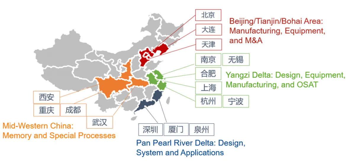
The China IC Ecosystem Report, a comprehensive report for the IC manufacturing supply chain, reveals that front-end fab capacity in China will grow to account for 16 percent of the world's semiconductor fab capacity this year, a share that will increase to 20 percent by the end of 2020. With the rapid growth, China will top the rest of the world in fab investment in 2020 with more than $20 billion in spending, driven by memory and foundry projects funded by both multinational and domestic companies, according to the new report released today by SEMI.The report also shows that IC Design remained the largest semiconductor sector in China for the second year in a row with $31.9 billion in revenue in 2017, widening its lead over the long-dominant IC Packaging and Test sector. The ascent of China’s IC Design sector comes as the region’s equipment market is expected to claim the top spot in 2020 for the first time on the strength of the continuing development of its domestic manufacturing capability. China’s maturing domestic fab sector is also benefiting domestic equipment and materials suppliers. Both groups continue to see gains in their product offerings and capabilities, particularly in silicon wafer production. The China IC Ecosystem Report is produced by SEMI, the global industry association and provider of independent electronics market research.The more than RMB140 billion (US$21.5 billion) accumulated by the National IC Fund, a critical component of the 2014 National Guideline to address China’s semiconductor trade deficit, has spurred rapid gains throughout the region’s IC supply chain. Semiconductors are China’s largest import by revenue. Phase 2 of funding aims to raise another RMB150-200 billion ($23.0-$30.0 billion).Encouraged by the National Guideline and favorable policies, skilled overseas talent is returning to China, triggering an explosion of domestic IC Design start-ups that are benefiting from access to investment and favorable policies, the report shows.Other highlights from The China IC Ecosystem Report include: Currently 25 new fab construction projects are underway or planned in China. 17 - 300 mm fabs are being tracked as part of this investment and expansion activity. Foundry, DRAM and 3D NAND are the leading segments for fab investment and new capacity in China. China’s IC Packaging and Test industry is also moving up the value chain by enhancing its technology offerings through mergers and acquisitions and building advanced capabilities to entice international integrated device manufacturers. China’s IC materials market, currently dominated by Packaging materials, became the second largest regional market for materials in 2016, a position it solidified in 2017. China’s materials market is expected to grow at a 10 percent CAGR from 2015 to 2019, driven primarily by the region’s new fab capacity ramp in the coming years. Fab capacity will expand at a 14 percent CAGR during that period. The China IC Ecosystem Report covers the latest semiconductor supply chain and market developments including the rise of China’s IC industry, national and local government policies, public and private funding, and their implications for China's IC supply chain. The report also compares key domestic companies and their international peers segment by segment. To learn more and get a sample of the report, visit http://www.semi.org/en/china-ic-ecosystem-report.Eugenia is a Senior Product Marketing Manager at SEMI.
Read More
IntroductionStarting July 4, 2022, PFOA (Perfluorooctanoic acid) levels in semiconductor manufacturing and related equipment (SMRE), including replacement parts, entering the European Union (EU) will be restricted to 25 ppb per component (or any part thereof). Semiconductor equipment components (and the parts thereof) of particular concern include fluid tubing and fittings, pipe/seal tape, wire and cable insulation, filters, valves, tanks, panels, reaction vessels and o-rings; if they are made from fluoropolymers or fluoroelastomers.When PFOA is used as an aid to the manufacture fluoropolymers such as PTFE, PFA, PVDF or fluoroelastomers such as FKM and FFKM (collectively referred to as fluoromaterials), an unintended PFOA residue can be trapped within the fluoromaterial. Buyers of components used in SMRE are usually unaware of the processing method used for any fluoromaterials they may contain, and, as a consequence, the potential for PFOA residue. This lack of information about potential PFOA residues could result in regulatory enforcement actions and restricted market access, particularly in the EU.The impact of restrictions on fluoromaterials used in SMRE has been introduced in previous SEMI articles ‘Fluorinated Compound Restrictions May Trigger Costly Equipment Changes’ and ‘Fluorinated Substance Restrictions Triggers Costly Equipment Changes.’PFOA and its related compounds, such as the ammonium salt APFO (collectively called PFOA in this article), are recognized internationally as hazardous chemicals and are now targeted for regulatory restriction in the U.S., Taiwan, Canada and the EU. The UN Stockholm Convention on Persistent Organic Pollutants (POPs) is also considering listing PFOA, which could lead to additional international restrictions.The SEMI EHS Division PFOA Compliance Working Group has been working to understand: The likelihood of PFOA residue entering the supply chain of new components The residual level of PFOA in fluoromaterials produced prior to the phase out of PFOA by some manufacturers The impact of PFOA residue on the secondary equipment market This SEMI resource page, ‘Elimination of PFOA from the Equipment Supply Chain,’ and the supporting FAQ contain the Working Group’s key findings and conclusions.PFOA in the Fluoromaterial Supply ChainSignatories to the U.S. EPA Stewardship Program, which include FluoroCouncil members, eliminated PFOA from their manufacturing processes by 2013. However, other fluoromaterial manufactures – particularly in China, Russia and India – might still use PFOA and pose a significant risk to the worldwide supply chain.China, the world’s largest fluoromaterial producer, accounts for 53 percent of global production of PTFE and 38 percent of worldwide production of PVDF, FEP and FKM. An estimated 75 percent to 85 percent of fluoromaterials are manufactured using PFOA in China. Fully 25 percent of these fluoromaterials are exported, primarily to the U.S, Japan, EU and India. What’s more, finished goods made from or containing fluoromaterials that might be used as components in SMRE are exported from China.Documentation that traces fluoromaterials through the supply chain back to the original fluoromaterial manufacturer is key to meeting the PFOA regulatory requirements. This traceability can be straightforward in cases when an SMRE manufacturer directly specifies the use of a fluoromaterial in a custom-fabricated fluoromaterial component. However, for off-the-shelf components (e.g., cable ties, wiring insulation, tubing) or the components assembled from these components (e.g., controllers), the complexity and dynamics of the supply chain makes traceability back to the original fluoromaterial producer almost impossible.Residual PFOA Levels If, or how much, PFOA/APFO residue is contained in a fluoromaterial depends on the manufacturing process. Details of the manufacturing processes are proprietary and vary widely. Post manufacturing thermal treatments, such as sintering, extrusion, and molding, can result in the rapid thermal decomposition of APFO above 250C, but PFOA is significantly more stable. The temperature and time of thermal treatments is also proprietary and varies depending on the type of fluoromaterial and what is being made.This variability makes it impossible to estimate the likely level of trapped PFOA or APFO in a finished component or a part thereof. It is unwise to use data on the level of residue made known for one case to extrapolate the level of residue across the fluoromaterial industry. However, an industry-wide range on the order of 1ppm-10ppm (nearly 1000 times the EU limit) is suspected. Testing for the presence of PFOA/APFO at 25ppb in components is also problematic as there is no standard test method, and results among the custom methods developed in each test lab may vary.Given this uncertainty in test methods, a system of supplier declarations warrants consideration.Impact on Secondary (Used) EquipmentThe EU REACH restrictions apply to SMRE and replacement parts placed on the market at any time (not just initial placement – known as “first placing on the market”). For fluoromaterial components manufactured prior to 2013, there is a higher likelihood of residual PFOA/APFO levels exceeding the 25ppb limit of EU REACH. In principle all the SMRE components containing fluoromaterials should be investigated, and those containing PFOA above 25ppb must be replaced before the SMRE can be legally placed again on the EU market. Companies (e.g., semiconductor manufacturers) in the EU who wish to sell used equipment within the EU will be required to demonstrate the used equipment is in compliance. Selling older used equipment would likely be unprofitable after necessary investigations and component replacements are completed.Next StepsWhile the EU semiconductor manufacturing industry heavily depends on the secondary (used) equipment market, EU regulators may be unaware of the PFOA restriction’s damaging impact to this market. The EHS Division PFOA Working Group, in conjunction with SEMI Europe, is now considering how to bring this concern to the attention of regulators and to collaborate and lobby for effective changes including possible modifications to the EU Persistent Organic Pollutants (POPs) regulation.
Read More
Tracking toward even stronger growth than forecast last year, 200mm fabs worldwide are gearing up to add more than 600,000 wafers per month from 2017 through 2022, an 11 percent growth rate that will lead to a new high of 6 million wafers per month by the end of 2022, according to the SEMI Industry Research and Statistics group in its fourth update of the Global 200mm Fab Outlook report. See chart below. All told, 56 older and newer facilities will add capacity, with the MEMS, power, logic and foundry segments contributing the most. To help meet rising demand, new fabs are under construction. Only six facilities plan to reduce capacity. The global 200mm fab count will increase from the 2017 level of the 194 fabs covered in the report to 203 by 2022. See chart. During the five-year forecast period, China, at 44 percent, is expected to account for the greatest growth, followed by Southeast Asia (19 percent), Taiwan (10 percent) and the Americas (8 percent). However, with strong demand for new 200mm fab equipment, the used 200mm fab equipment market has pretty much dried up. What’s more, the availability of key tools and spare parts has become a primary concern for many device makers. These headwinds notwithstanding, many companies remain bullish with plans to add more capacity. The forecast growth of 600,000 wafers per month may ultimately be a conservative estimate. SEMI’s Global 200mm Fab Outlook report lists more than 300 facilities and lines managed by more than 150 companies, providing details on product type, investment, technology and capacity plans by companies and fabs. The fourth update of the Global 200mm Fab Outlook report covers data and predictions from 2011 through the end of 2022, including milestones, detailed investments by quarter, product types, technology nodes and capacities down to fab and project level. Click here for the Global 200mm Fab Outlook Sample Report. Learn more about other SEMI fab databases at www.semi.org/en/MarketInfo/FabDatabase. Christian G. Dieseldorff is director of Industry Research and Statistics, SEMI, Milpitas, California.
Read More
Powerful winds of change are re-shaping the semiconductor industry as it flexes and re-positions to power a new wave of growth on the back of emerging applications. Today, the industry is thriving, with growth expected to continue through 2019 even as Moore’s Law – the trusty doubling of transistors roughly every two years – begins to pump the brakes. Product mix and production technology are shifting as the dominant smartphone and PC markets, having seen their growth peaks, start to give way to large markets with relatively low semiconductor penetration, such as automotive.What’s more, new potentially ubiquitous technologies and platforms such as AI, blockchain and smart manufacturing are redefining market dynamics and the semiconductor ecosystem that underlies them.Troublingly, the most significant threats to the continued growth of the semiconductor industry are not of its own making. Macroeconomic trends and trade policy disputes loom.These were some of the key takeaways from the SEMI Market Symposium kicking off SEMICON West in San Francisco this week. Following is a deeper look.Semiconductor MarketThe consensus view, reflected in forecasts presented by Clark Tseng of SEMI and Bob Johnson of Gartner, is that the semiconductor industry could top $500 billion in 2019 after reaching $400 billion in 2017. According to Gartner, smartphones and PCs will continue to account for large parts of the market, but will be displaced as major drivers of market growth by the emergence of industrial, automotive and, to a lesser extent, storage, from 2017 to 2022. Johnson noted that while communications and data processing applications drive logic device demand, average sales prices (ASPs) are a bigger contributor to revenue growth than unit growth.Leading-edge processors are a big part of the ASP picture, with equipment costs increasing ~20 percent per node. One challenge is that as Moore’s Law loses steam, leading logic producers are increasingly going their own way with new production technology. The volatile DRAM market – now in a “super cycle,” according to Tseng, and expected to peak in 2019 – has been stoking memory market growth.Initially, supply shortages fueled memory price increases as three of the four leading memory makers invested in flash rather than DRAM capacity. However, memory prices have been more recently been lifted by technology complexity, particularly as DRAM has moved to 3D architectures. The good news is that pricing, at long last, appears to be driven by value.Automotive MarketWith automotive accounting for less than 10 percent of semiconductor demand, there is room for growth. Rudy Burger of Woodside Partners noted that while the end market for automobiles is growing slowly, at 3 percent CAGR, the market size is nearing 100 million units. In market segments such as electric vehicles, the semiconductor content exceeds $1,000 but can be much higher.For example, the BMW i3 sports over $4,000 in semiconductor content. Burger said connectivity, autonomous driving and shared mobility services are also key opportunities for semiconductors to deepen their penetration in automobiles. For instance, the auto market for cameras, is expected to grow from $2 billion in 2017 to $6 billion in 2022.On average, high-end vehicles feature over $1,000 in semiconductor content, whereas low-end vehicles hover in the $400 range, said Anand Srinivasan of Bloomberg. Because the automotive market is segmented by function or subsystem, with different suppliers focusing on different areas, there is little supply concentration. Srinivasan also pointed out that because of significant differences in their objectives, automotive safety and automation systems should be developed separately.BlockchainThe chief benefit of blockchain is the trust it begets among all parties to a digital transaction through four fundamental features, said David Treat of Accenture: The tracking of provenance (knowing who has touched data, and what has happened to it) Tamper evidence (knowing if someone has tried to change the data) Control (which data elements to share with which parties) Security at the data element level While most of the hype over blockchain focuses on tokenized assets and ledgers (bitcoin and other cryptocurrencies), the fundamental application in the semiconductor industry is sharing trusted access to reference data at the data element level. This ability to provide shared trust can reduce costs throughout the supply chain and across enterprises. For example, future blockchain implementations will offer a full ecosystem view to any supply chain participant. While blockchain has typically been deployed through centralized control or platforms, peer consortia, such as SEMI, could help weave the benefits of blockchain through various ecosystems by enabling equipment and material suppliers, device manufacturers, designers and system integrators to share business and technical information securely and, if desired, anonymously.Global and Macroeconomic TrendsThe biggest threats to the continued growth of the semiconductor industry are exogenous. After a decade of steady recovery since the financial crisis, the global economy appears to be heading for a slowdown. Duncan Meldrum of Hilltop Economics made the case that the global economy is at or just past the peak of the business cycle, and semiconductor equipment is past the peak.A key indicator of a looming recessionary is the movement toward an inverted yield curve, in which long-term interest rates fall below short-term rates – a phenomena that could materialize this year or next.The increasingly heated trade climate, marked by high-stakes confrontations between the U.S. and China, threatens complex supply chain arrangements, though mercurial policy statements could do even more harm than stiffer trade tariffs. Underscoring competing interests between the U.S. and China and the unpredictability of their relations, Robert Maire of Semiconductor Advisors pointed out that, in 2019, 60 percent of all semiconductors are expected to be used in China, deepening the dependency of several U.S. semiconductor companies on China.Paul Semenza, for SEMI Industry Research and Statistics
Read More
Christian G. Dieseldorff, Industry Research Statistics Group, SEMI (June 12, 2018)The semiconductor industry is nearing a third consecutive year of record equipment spending with projected growth of 14 percent (YOY) in 2018 and 9 percent in 2019, a mark that would extend the streak to a historic fourth consecutive growth year, according to the latest update of the World Fab Forecast report published by SEMI. The industry last saw four consecutive years of equipment spending growth in the mid 1990s.Korea and China are leading the growth, with Samsung dominating global spending and ascendant China on a fast, steep rise, surging ahead of all other markets. See figure 1.Figure 1: equipment spending by region (includes new and refurbished)Samsung is expected to reduce equipment investments in 2018. Despite the ebb, the company still accounts for a dominant 70 percent of all investment in Korea. At the same time, SK Hynix is increasing its equipment spending in Korea.China’s equipment spending is forecast to jump a whopping 65 percent in 2018 and 57 percent in 2019. Notably, 58 percent of investments in China in 2018 and 56 percent in 2019 stem from companies with headquarters in other regions such as Intel, SK Hynix, TSMC, Samsung, and GLOBALFOUNDRIES. Domestic, Chinese-owned companies – backed by large government initiatives – are building an impressive number of new fabs that will start equipping in 2018. The companies will double their equipment investments in 2018 and again in 2019.Meanwhile, other regions are also ramping up investments. Japan is beefing up equipment spending by 60 percent in 2018, with the largest increases by Toshiba, Sony, Renesas and Micron.The Europe and Mideastern region will boost investments by 12 percent in 2018, with Intel, GLOBALFOUNDRIES, Infineon and ST Microelectronics as the largest contributors. Southeast Asia will increase investments by more than 30 percent in 2018, although total spending is proportionately smaller than in other regions owing to its size. The main contributors are Micron, Infineon and GLOBALFOUNDRIES, though companies including OSRAM and ams are also increasing investments.The SEMI World Fab Forecast, which also includes information on other companies, covers data and predictions through the end of 2019, including milestones, detailed investments by quarter, product types, technology nodes and capacities down to fab and project level.Learn more about the SEMI fab databases at:www.semi.org/en/MarketInfo/FabDatabase and www.youtube.com/user/SEMImktstats.
Read More
Broad Global U.S. Electronic Supply Chain GrowthThe first quarter of this year was very strong globally, with growth across the entire electronics supply chain. Although Chart 1 is based on preliminary data, every electronics sector expanded – with many in double digits. The U.S. dollar-denominated growth estimates in Chart 1 have effectively been amplified by about 5 percent by exchange rates (as stronger non-dollar currencies were consolidated to weaker U.S. dollars), but the first quarter global rates are very impressive nonetheless. U.S. growth was also good (Chart 2) with Quarter 1 2018 total electronics equipment shipments up 7.2 percent over the same period last year. Since all the Chart 2 values are based on domestic (US$) sales, there is no growth amplification due to exchange rates.We expect continued growth in Quarter 2 but not at the robust pace as the first quarter.Chip Foundry Growth ResumesTaiwan-listed companies report their monthly revenues on a timely basis – about 10 days after month end. We track a composite of 14 Taiwan Stock Exchange listed chip foundries to maintain a “pulse” of this industry (Chart 3).Chip foundry sales have been a leading indicator for global semiconductor and semiconductor capital equipment shipments. After dropping to near zero in mid-2017, foundry growth is now rebounding.Chart 4 compares 3/12 (3-month) growth rates of global semiconductor and semiconductor equipment sales to chip foundry sales. The foundry 3/12 has historically led semiconductors and SEMI equipment and is pointing to a coming cyclical upturn. It will be interesting to see how China’s semiconductor industry buildup impacts this historical foundry leading indicator’s performance. Passive Component Shortages and Price IncreasesPassive component availability and pricing are currently major issues. Per Chart 5, Quarter 1 2018 passive component revenues increased almost 25 percent over the same period last year. Inadequate component supplies are hampering many board assemblers with no short-term relief in sight.Peeking into the FutureLooking forward, the global purchasing managers index (a broad leading indicator) has moderated but is still well in growth territory.The world business outlook remains positive but requires continuous watching!Walt Custer of Custer Consulting Group is an analyst focused on the global electronics industry.
Read More
Large semiconductor fabs can devour electricity at clip of 100 megawatts per hour -- enough to power 50,000 homes1 and, according to a McKinsey study, more than automobile plants and oil refineries consume. So ravenous is their electricity consumption that some fabs have resorted to building their own captive power plants. Oversize fabs, depending on their location and local rates, can run up utility bills as high as $25 million each year, with electricity accounting for up to 30 percent of operating costs.Fabs use electricity to power HVAC, run cooling water, and for basic infrastructure. But the vast majority of electricity is gobbled up by semiconductor manufacturing process tools and their sub-fab support equipment such as vacuum pumps and abatement systems. In a typical fab, as much as 44 percent of the electricity is consumed by the processing equipment2. It’s not so hard to imagine. Etch and deposition tools need power to strike and sustain plasma, with multiple 1,000+ Watt RF power supply feeds per chamber and four, six or more chambers per tool, and vacuum pumps spinning and abatement running. The power load adds up quickly. Watts and WattsThe good news is that process tools aren’t processing wafers all the time. The bad news is that, in the past, there was no good way for the fab to know when process tools and support equipment weren’t running processes. Turning equipment off, or reducing power when not processing, wasn’t coordinated and standby states weren’t defined for readiness for a seamless power-up and return to processing. So what to do? Take action. That just what industry volunteers did when they met within SEMI’s Standards program and defined an equipment “idle mode” (SEMI E167 and SEMI S233). More recently, a SEMI Standard (SEMI E1754) was developed to define energy saving modes – how process tools communicate with sub-fab equipment, to reduce utility consumption when wafers are not being processed by the tool. Importantly, it also provides guidance on the standby state to return to full performance when the tool is needed to process wafers.5Good to be IdleThe semiconductor industry is now increasingly adopting a “smart idle” approach using these SEMI Standards. Fabs implementing these standards to take advantage of process tool idle periods can save more than 4.3 million € annually, according to AIS Automation modeling.6 This study also points to a savings of more than 16,000 tons of CO2 per year, the equivalent of taking more than 10,000 cars off the road.Who knew that recognizing when to be idle could bring such big rewards? If only I could apply that to my own life, but, for now, I will have to leave it to the fabs. SEMI International Standards volunteers make a huge difference to our industry every day. If you want to join the over 5,000 SEMI Standards volunteers (or join SEMI’s Sustainable Manufacturing eForum), with representation from over 2,000 companies, it’s free! Don’t be idle for this one, click here to join! http://www.semi.org/en/standards/P041367 1Bringing Energy Efficiency to the Fab, McKinsey 20132http://semiengineering.com/saving-energy-in-the-fab/3SEMI E167-1213 - Specification for Equipment Energy Saving Mode Communications (EESM)http://ams.semi.org/ebusiness/standards/SEMIStandardDetail.aspx?ProductID=211 DownloadID=32573SEMI S23-0813 - Guide for Conservation of Energy, Utilities and Materials Used by Semiconductor Manufacturing Equipmenthttp://ams.semi.org/ebusiness/standards/SEMIStandardDetail.aspx?ProductID=211 DownloadID=31094SEMI E175-1116 - Specification for Subsystem Energy Saving Mode Communication (SESMC)http://ams.semi.org/ebusiness/standards/SEMIStandardDetail.aspx?ProductID=211 DownloadID=38765http://electroiq.com/blog/2017/06/how-semi-standard-e175-is-saving-energ...6SEMI Standards a Potential Help for Saving Energy, Bert Mueller, AIS Automation 2016
Read More