downloadGroupGroupnoun_press release_995423_000000 copyGroupnoun_Feed_96767_000000Group 19noun_pictures_1817522_000000Member company iconResource item iconStore item iconGroup 19Group 19noun_Photo_2085192_000000 Copynoun_presentation_2096081_000000Group 19Group Copy 7noun_webinar_692730_000000Path
Skip to main content
Default Banner Image

IoT

On the day I joined SEMI in March of 2017, I was filled with excitement to be on-boarding at a time when great, leaping strides in innovation were driving the rapid expansion of our ecosystem. In my many conversations with members that followed, I was not surprised that a vast majority ranked among their top concerns the persistent challenge of attracting, training and retaining the talent needed to grow their businesses. Later that year, I raised the global talent shortage issue in my article Securing Talent to Connect, Collaborate and Innovate. As an industry veteran I knew that the decades-long workforce development challenge will only worsen with the proliferation and increasing complexity of technology.Innovation has never been more technology-intensive. Developing the technology and producing the components required for applications powering next-generation communications (5G), artificial intelligence (AI) and machine learning, autonomous vehicles, and the Internet of Things (IoT) require bright minds in diverse fields of science to fill critical positions in the global electronics manufacturing industry. Today, that talent struggle is acute, threatening to undermine our industry’s potential to grow to $1 trillion by 2030.The electronics industry needs a comprehensive, integrated program to build the talent pipeline. The program should inspire school-age children to adult learners to pursue careers in this great but underrecognized industry. It needs to shine a spotlight on career opportunities. It must prepare workers with standardized skills sets transferable across the industry. And it must connect trained workers with hiring companies.SEMI is uniquely positioned to deliver this solution. Launched almost two years to the day after I joined SEMI, SEMI Works is SEMI’s branded workforce development initiative. We realize that trade associations don’t create jobs. Their members do. Think of SEMI Works as SEMI’s commitment to build and maintain the needed infrastructure – the talent pipeline. SEMI Works is comprehensive. The program, supported by SEMI members, is a wide-ranging effort by our Global Advocacy team to ensure education is demand-driven, training programs better meet the needs of the industry, more people pursue careers in electronics and our members have access to the talent pool that we are cultivating. With SEMI Works, SEMI is developing scalable solutions to improve connections among training and education providers, prospective workers and the industry. Key features of SEMI Works will include SEMI-certified education courses and training programs linked to industry requirements and skills credentialing for workers.SEMI Works starts with raising awareness of SEMI-certified programs as a key bridge connecting prospective talent, the industry and applicable training and education programs. Growing awareness of the programs will enable SEMI to build an extensive database of employers and qualified talent and link both to the right training. SEMI will continue to drive and endorse programs that help meet member needs throughout the education continuum – from K-4 to higher education and adult training. But the infrastructure and ecosystem required to support and scale these programs is the key for all of us to win together. At a high level, SEMI Works consists of several important components: Linking the required industry competencies to education and training course curriculum – Similar to the establishment of SEMI standards, SEMI will certify education and training programs that dovetail with the industry competency model. Initial certification and annual re-certification ensure continued updates, relevance and sustainability of the programs. SEMI will raise awareness of SEMI Works certified programs as the standard for meeting the industry’s talent requirements. Developing and maintaining the electronics industry competency model – Through established working groups and ongoing dialogue with our members, we are developing a competency model – a tiered matrix of required competencies used to link course curriculum to the talent needs of employers. The competency model consists of interpersonal and individual skills, academic and general industry requirements, advanced manufacturing competencies, and competencies by job. SEMI will establish and maintain the model with regular updates. Improving access to talent – Through SEMI Works, SEMI will build an extensive database that brings together programs, talent and employers. People and organizations opting into a SEMI-certified program or acquiring a SEMI program certification will be part of the SEMI database. Job seekers will be able to set up a profile and resume and search for training and employment opportunities, and employers will search the talent pool – much as job-search sites work today – assured of a skills match based on the SEMI certification. I am passionate about education and proud of all of SEMI’s efforts. I am especially proud of the work we are doing to help provide a pathway to meaningful careers for children and adults all around the world. We no longer have the luxury of a piecemeal approach to training and education.It is my hope and belief that SEMI Works, together with our efforts to improve diversity and inclusion in the workforce, will be SEMI’s lasting mark on the global electronics industry.Ajit Manocha is president and CEO of SEMI.
Read More
How are flexible electronics impacting the automotive sector? How will medical diagnostics and life sciences be changing with the advent of flexible, conformable electronics? How does space exploration intersect with the continued development of flexible sensors and Internet of Things (IoT) systems? The upcoming 2019FLEX Japan / MEMS SENSORS FORUM in Shinagawa, Tokyo, May 22-23, 2019, will explore these questions and more. The event, the third FLEX Japan, is expected to gather 300 designers, technologists, researchers, analyst and product developers to hear presentations, discuss their approaches, and create connections. The transformation of the automotive industry will receive special attention with speakers from Yole Développement and a deep exploration of the new sensor form factors and capabilities. Professor Shoji Kawahito of Shizuoka University will discuss the impact of image sensors on automotive LIDAR, night vision and monitors for the driver and passengers. Dr. Yoshifumi Sakamoto of IBM Japan will share his views on key trends in smart transportation and what they mean for the supply chain. Beck Oh, president and CEO of PNI Sensor, will share how parking sensors are transforming our driving – and parking – experience. Hideo Fukunaga, project manager for Velodyne LiDAR, will discuss his work using LIDAR, often seen as the most promising and the most difficult and expensive component of autonomous driving. Jerome Joimel, CTO of ISORG, will discuss integration of organic image sensor behind display.Medical and home electronics devices are moving out of their boxes and hospitals, and flexible electronics, new sensor designs and new power options are playing a major role in that transformation. Jenax, Kobe University, Toyo University, Osaka University, and Daiwa House are just some of the presenters in this area. Researchers are steadily overcoming key technology hurdles, such as electronic interconnects between soft and rigid surfaces, and energy harvesting techniques for no-power devices, as well as ultra-thin RF components, and advanced microfluidic systems. Space, the final frontier, will be the backdrop for the general keynote talk of Mayya Mayyappan, chief scientist for exploration technology at NASA’s Ames Research Center. His team is investigating new printed and flexible sensors and electronics that can be printed in zero-gravity and how these devices will enable IoT.The only event in Japan focused on flexible and printed electronics, with special focus on the complementary areas of sensors and MEMS, 2019FLEX Japan / MEMS SENSORS FORUM provides an excellent opportunity to meet with industry players considering integration and application of new form factor electronics. More than 20 exhibitors will showcase the building blocks for conceptualizing and designing new products immediately.Register now!
Read More
Creating a custom Internet of Things (IoT) IC is challenging because it involves multiple design domains (digital, analog and RF). Creating a sensor-based IC that combines electronics that use the traditional CMOS IC design flow with a MEMS sensor on the same silicon die, however, can seem impossible. Couple the co-design and verification challenges with a lack of traditional process design kit (PDK) support for MEMS, and you have a tough road to travel to get your IoT designs to market.What can we do to make the sensor-based IoT design community successful?Understanding the ChallengesThe sensor-based IoT IC typically features a MEMS sensor (and optional actuator) that interact with the real world. Analog and digital circuitry processes the signals and sends them to a CPU. The CPU provides the “smarts” to process the data from the sensor and then sends processed data via a radio to the Internet; alternatively, the CPU could activate the actuator. A typical sensor-based IoT IC (Source: Mentor: A Siemens Business) Based on the complexity of the system, designers face many co-design challenges: Analog design requirements imposed by MEMS: MEMS devices often require high voltages and multiple power supplies; they emit small signals that need amplification and conditioning; and they are sensitive to the environment and require calibration. Design flow interactions: Parasitics from MEMS devices might affect circuits and vice versa. Circuit designers need MEMS models for impedance and timing. Integration: MEMS devices operate at different timescales than circuits, which adds a layer of complexity. Compounding the problem is a lack of MEMS PDKs and methods to tie together ICs and MEMS PDKs for integration and cross-verification. After conquering the co-design challenges, the design team has to address mixed-domain simulation challenges that include: Simulating the system: This requires verification of MEMS, digital, analog and RF circuitry with embedded software that runs on the CPU. Timescales: These vary widely, from a single deflection of the MEMS transducer in femtoseconds to a seconds-long simulation of the embedded software performing a measurement and transmitting data. Simulation time: Simulation of a behavioral digital design is extremely fast. However, the system simulation requires stand-in models that incorporate the behavior of the analog and MEMS block to simulate in an acceptable amount of time. The challenge of timescales for co-simulation. (Source: Mentor: A Siemens Business) MEMS is the KeyThe reality is that it’s the MEMS device that adds extra complexity to the sensor-based IC design and verification flow. To amplify the problem, the MEMS manufacturing process is not nearly as mature as the standardized IC process. For example, the standardized IC process includes ready-made PDKs that include everything designers need to move through design and verification flows. Foundries often provide soft and hard IP to quickly build-out design, and EDA tools provide high levels of automation enabled by abstraction and a standardized IC flow. How will MEMS-based design evolve?MEMS-based design must catch up to the standardized IC process. The first step is providing MEMS PDKs that include: Multi-physics domain design rules and material properties Packaging information Wafer and bonding information Fabrication information We must also tackle issues associated with these PDKs, including: Ownership, distribution and maintenance of the PDKs Consensus on the contents of the PDKs Merging of CMOS and MEMS PDKs The industry needs to move toward standardized MEMS manufacturing processes with available PDKs. Companies must provide IP and recommend structured design methods for co-design and verification of ICs that incorporate MEMS. How can EDA help with these flows?The EDA ContributionEDA companies must work with teams in the MEMS IC co-design space, collaborating with MEMS fabricators to help enable PDKs. By incorporating PDK support within their own tools, EDA companies can provide an integrated custom IC flow that allows teams to design and verify MEMS-based ICs. For details about this flow, click here to download the Mentor whitepaper: Fusing CMOS IC and MEMS Design for IoT Edge Devices.Greg Lebsack brings 25 years of executive and technical management experience — along with a proven track record of building strong teams and delivering predictable results — to his role as general manager of the ICDS division of Mentor, a Siemens Business. Lebsack joined Mentor in 2015 after that company acquired Tanner EDA, where he was president. Prior to Tanner EDA, he held management and technical positions in a number of different industries and companies, including Sprint, General Electric and McKinsey Co. Greg holds a bachelor’s degree in business administration from Northern Arizona University.Greg Lebsack recently presented on the topic of Integrated Co-design of MEMS/IC at the MEMS Sensors Technical congress, a technical conference organized by the MEMS Sensors Industry Group.
Read More
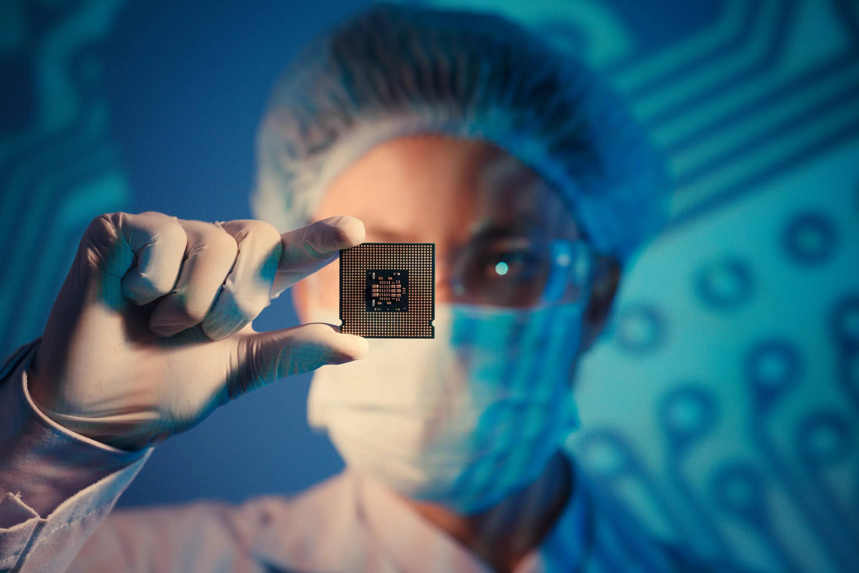
MedTech, autonomous driving and other disruptive technologies will be in focus at the SEMI Industry Strategy Symposium (ISS Europe), 31 March - 2 April 2019 in Milan, Italy, as top European executives, researchers and academics gather to explore solutions to the region’s most pressing strategic, economic and social challenges. Ahead of ISS Europe, SEMI spoke with Mark Purdy, managing director and chief economist at Accenture Research, about Accenture’s Business Futures – four different future worlds set in 2025 based on the collision of trends across demographics, geopolitics, technology, and economics – and what these futures will mean for markets, workforces, operating models and industry value chains. SEMI: At ISS Europe in Milan, you will kick off the symposium highlighting market opportunities of the digital economy and how companies must adapt to competitive challenges. What inspired Accenture’s Business Futures four world scenarios?Purdy: The impetus for our Business Futures really stemmed from a certain dissatisfaction with current approaches to thinking about the future. We were struck by the following puzzle. First, there is no shortage of techniques for looking at the future, from forecasting to trends analysis to conventional scenarios. Second, most decision-makers have more or less the same access to information on global trends. Yet, time and again, we hear stories of businesses going bust or facing major challenges precisely because they failed to anticipate major changes in their industry.The paradox is that we have so much information, but so little real understanding of how the future actually unfolds. So that set us thinking about how to develop a new approach, based on a combination of detailed trend analysis, expert input and creative storytelling – which is what we call “Business Futures.” SEMI: Of demographics, geopolitics, technology, and economics, which trend do you see as particularly critical?Purdy: Actually, the essence of our Business Futures thinking is that it is the collision or combination of different trends – across economics, technology, demography, etc. – that shapes future outcomes, rather than individual trends per se. To a certain extent we tend to become fixated on specific trends and this can lead us astray or cause bad decision-making. For example, in the early 2000s many people saw very favorable trends in the U.S. economy – strong capital inflows, rapidly rising consumer spending, surging stock markets, and rising home ownership rates. Each trend in isolation looked strong and sustainable. But we failed to see how the combination of these trends was fueling risky financial innovation that would eventually lead to the financial crisis and great recession.Technology of course is a key trend. We are seeing tremendous advances in next-wave technologies such as robotics, machine learning, intelligent objects, 5G and virtualization. But we can only truly understand the impact of the technologies – and the business opportunities and challenges they create – by viewing them against a wider backdrop of changes in society, demography, geopolitics and economics. That is what Business Futures strives to do.SEMI: What will these different futures mean for markets, workforce, operating models and industry value chains?Purdy: There will be profound changes in how we think about all of these areas. Markets will become much more personalized and interactive. Technology will be increasingly integrated with humans, fueling innovation in areas such as personalized healthcare and preventative medicine. Our notions of distance and capacity will be upended, as new virtualized services enable new ways of reaching underserved customers. Consumers will become increasingly involved in the creation and design of products and services. New methods of innovation, powered by AI and virtualization, will come to the fore. New entrants will come from unexpected quarters, enabled by new technology. The upshot will be massive disruption and disintermediation of value chains across many sectors.SEMI: What can Europe do to prepare?Purdy: There are no simple answers, and the correct course will vary by country, but there are some basic things to get right. First, different countries need to understand their comparative advantage – for example, whether it is in services, new technologies, advanced manufacturing or resources – and work with the grain of these different futures. Second, countries need to ensure that they have the basic conditions – regulation, organizational adaptability, workforce flexibility, skills, and innovation infrastructure – to capitalize on the productive potential of new technologies such as AI, virtual reality, and the Internet of Things (IoT). Third, we need to create educational systems and workforce learning methods that emphasize creativity, problem solving and innovation – precisely the skills that will be most needed in an age of intelligent machines. SEMI: What are your expectations for the summit in Milan and for the future?Purdy: I’m very much looking forward to the ISS Europe Summit in Milan. As an economist, I believe we are at a pivotal moment in the semi-conductor industry, driven by waves of technological change and rising geopolitical frictions and uncertainty. With so many industry leaders and experts coming together at the Summit, I’m confident that our discussions will help point a way forward!Mark Purdy is managing director of economic research at Accenture Research. His research examines issues at the intersection of economics, technology and business. He has published widely in tier-1 media and specialised publications on topics such as China’s economy, emerging-market geographic strategy, inclusive economic growth, business futures and the economic impact of new technologies such as the Internet of Things and artificial intelligence. A graduate of Trinity College Dublin, he speaks on these topics at conferences and seminars around the world.Serena Brischetto is a marketing and communications manager at SEMI Europe.
Read More
For nearly two decades, Sean Ding, CTO and chief scientist of Alibaba Cloud IoT, has worked in software and algorithm architectures, sensing, semiconductors, systems and cloud computing – all areas that have contributed to the rise of the Internet of Things (IoT). It’s no surprise, then, that Alibaba is leading next-generation innovation for the IoT. Ding will bring his expertise to his role as moderator of Brave New World - MSIG Conference on AI+IoT 2019, a half-day forum March 20, 2019, at SEMICON China in Shanghai, China. Maria Vetrano of SEMI spoke with Ding about technologies key to the IoT era including MEMS, sensors, artificial intelligence (AI), edge gateways and cloud computing. SEMI: MEMS sensors are widely used in IoT devices. What is the relationship between AI and MEMS sensors?DING: While MEMS sensors and AI will increasingly co-reside in end-user devices, I do not recommend adding AI next to the sensor (in the same package). That’s because designers continue to use the ASIC for signal conditioning, so A/D converters are still required. Rather, we should look to edge gateways to carry the majority of the workload, including deep learning, because this reduces system complexity and power consumption.SEMI: Why are smarter sensors shifting data processing and analytics to the edge of IoT devices?DING: Data processing and analytics are very important for IoT devices, but we need to focus on understanding the data, parameter calibration and more. The MEMS sensor industry should leave big data analytics to edge computing and cloud computing because AI requires deep learning, demanding a huge amount of data.The challenge is to find the sweet spot for data processing right next to the sensor element.SEMI: What is China’s evolving role in innovation in MEMS sensors for IoT devices?DING: At present, the MEMS community in China needs to figure out how to innovate instead of copying existing technologies, a low-margin business that will not help to grow the industry. One reason why I am so pleased to see the MSIG Conference on AI+IoT in China is that it will encourage greater creativity in the MEMS community in China, and this will ultimately lead to Chinese companies and R D institutions leading innovation rather than copying it.SEMI: What is the right approach to combining smart MEMS sensors with AI in IoT devices? Why is this important for both domestic Chinese and international markets?DING: Combining data from sensors with cloud-edge computing is the right approach. As sensor companies increasingly provide end-to-end solutions, such as “sensor+ firmware + SaaS + app,” we will realize easier and faster integration of sensors in IoT applications.This is incredibly important because China today is the world’s biggest market for IoT hardware. China has 2,000-plus design houses, 200-plus OEMs and thousands of distributors. That said, we still see a highly fragmented market that will benefit from a faster integration methodology.Faster integration of MEMS sensors and AI/machine learning for IoT hardware will benefit designers in international markets as well.SEMI: What do you hope MISG Conference on AI+IoT attendees will take away from the forum? DING: MEMS sensors are highly fragmented, reflecting the highly fragmented applications in which they play. The MEMS sensors industry should figure out how to provide one-stop-shopping solutions for vertical markets. This will speed the scalability of applications and expedite the growth of sensor production. Sean Ding (柯镇) will moderate Brave New World - MSIG Conference on AI+IoT 2019 at SEMICON China on Wednesday, March 20, 2019, at Kerry Hotel Pudong in Shanghai, China.This conference has been organized by the MEMS Sensors Industry Group (MSIG). Register today to connect with Sean Ding and featured speakers at the event.Speakers at the MSIG Conference on AI+IoT 2019 at SEMICON China include: Welcome and Introduction / 欢迎辞Carmelo Sansone, Director, MEMS Sensors Industry Group (MSIG), a SEMI technology community AI Needs Accurate Data – MEMS Sensors Can Provide It / MEMS传感器为人工智能提供真实数据Andrea Onetti, Group VP of Analog MEMS Group, GM of MEMS Sensor Division, STMicroelectronics Enhanced IoT Edge by Smart Sensors / 智能传感器助力IoT边缘智Bennini Fouad, Regional President Asia Pacific, Bosch Sensortec Horizon AI Processor Solution, Enable Industries in AI Time / 地平线AI芯片解决方案,赋能千万业Carl Zhang 张永谦, General Manager/VP, Smart Chip Solutions Division, Horizon Robotics Inertial Sensors in AI Applications / 运动传感器AI应用案例Ben Lee 李彬 , CEO, mCube Ultra-Low-Power Solutions: an Ecosystem Approach / 超低功耗的生态链解决方案Carlos Mazure, IEEE Fellow, Chairman Executive Director, SOI Industry Consortium High-Integrity, Fault-Tolerant Open Inertial Measurement Platform for AI-based Vehicle Automation / 适用于人工智能车辆自动控制的高集成及容错的惯性测量开放平台Dan Dempsey, Senior Director of Automotive, ACEINNA Maria Vetrano is a public relations consultant at SEMI.
Read More
SEMI has long promoted the industry collaboration that has contributed to the rise of the smart digital world we live in today. A world where data is being generated continuously by systems, gadgets, and sensors around us – often referred to as the Internet of Things (IoT). In our personal lives, most of us have smartphones, smart watches, smart TVs and smart cars, and we live in smart homes and smart cities generating huge amounts of data.In the work world, data and analytics are now influencing almost every industry including healthcare, government, financial services, construction and transportation. This data has the potential to transform our lives and make our world even smarter – if we can communicate and process this data, and use it to come up with actionable recommendations or actions. Artificial Intelligence (AI) and Machine Learning (ML) techniques have generated much excitement precisely because they offer us ways to realize the full value of data by harnessing it and transforming it into active intelligence.Data-intensive technologies are required to store, communicate and analyze data. And it all starts with innovation in microelectronics chips and systems spanning processors, memory, sensors, radios and other devices, presenting a huge opportunity to producers of these technologies. However, with Moore's Law beginning to slow, technology paths and innovation options are diverging. Companies must swiftly assess these options in order to develop competitive offerings. But the technological complexity and divergence makes it increasingly expensive or even unaffordable for many companies to track and pursue these options.The good news is that cost-effective early assessment is possible through pre-competitive collaboration that can produce new and often unexpected cross-disciplinary insights by overcoming traditional silos in industry and academia. Unfortunately, important collaborative industry platforms, such as the International Technology Roadmap for Semiconductors (ITRS), have folded, opening a collaboration gap in the global microelectronics ecosystem.As part of its mission to help companies connect, collaborate, and innovate, SEMI has built a collaborative, cross-supply-chain platform – the Strategic Innovation Platform (SIP). The goal is to provide early and comprehensive assessment of future technologies that are five to eight years away from commercialization. The assessment identifies not just technical barriers but also manufacturing and supply-chain constraints to implementing new technologies. SIP brings together the entire microelectronics ecosystem including strategic technology thought leaders, subject matter experts, technology and application developers, academia, researchers, start-ups and government. With more than 2,100-member companies spread across the global electronics manufacturing supply chain, SEMI is uniquely positioned to enable this critical collaboration. Award-Winning First ProjectThe inaugural SIP project assessed key drivers of future technologies. A key finding was that fast, efficient interconnects between devices and components are critical to the system performance important to customers and users, implying that system-level optimization is required. For data-intensive applications, interconnects have emerged as a key bottleneck for both performance and power in various circuits and systems in part because the slowing of Moore’s Law has decelerated advances in individual device performance, and in part because systems are becoming more complex, requiring heterogeneous integration.To address this challenge, SIP brought together industry experts from ASE Inc., Dow Chemical, Lam Research, Qualcomm and Xilinx to assess the future impact of interconnects for data-intensive applications. SEMI also involved Stanford University professors to collaborate on modeling and simulation. Through this unique cross-disciplinary collaboration, SIP developed a realistic model to evaluate the system-level performance of single-chip systems, as well as multi-chip systems – including traditional 2D packages, high-performance 2.5D systems that use interposers, and futuristic 3D systems. SIP also explored supply chain challenges in business continuity, manufacturability, Environment, Health and Safety (EHS) and the regulatory environment. SEMI worked with a broad range of industry partners to ensure that the model parameters accurately reflected realities on the design and factory floors to ensure usable results. Experimentation has become ever more expensive, with one industry player reporting that “it costs us $100 million to do a good experimental evaluation.” Accurate models can go a long way toward reducing the cost of technology assessment. The SIP collaboration produced key quantifiable insights including comparisons that highlight the benefits and limitations of various materials being explored for future interconnects, and of architectures under consideration for future data-intensive applications. For example, the current workhorse for artificial intelligence (AI) platforms – 2.5D technology – delivers a 4X improvement over 2D packaging but falls short of providing the orders-of-magnitude improvement that future AI/ML applications may require. These findings enable the industry to begin to identify ways to optimize 2.5D architectures, transition to 3D heterogeneous integration for performance-critical applications in the medium term, and to eventually evaluate new paradigms such as neuromorphic and quantum. The project findings were presented late last year in the form of two research papers at Electronics System-Integration Technology Conferences (ESTC) and International Microelectronics Assembly and Packaging Society (IMAPS) recently. One received the “Best Paper of the Session” award at IMAPS – a recognition that affirms the power of a collaborative platform such as SIP to produce valuable insights to address the growing technology complexity within the microelectronics industry. The microelectronics industry is on the cusp of a historic inflection point, where it could fuel the rise of emerging applications in AI/ML and IoT, and can grow into a trillion dollar industry over the next several years. More importantly, the industry is poised to help solve some of society’s most complex problems in areas including healthy living, climate change and transportation. No company can do this alone, and pre-competitive platforms such as SIP are key both to accelerating innovation through cross-disciplinary collaboration, and to reducing costs for individual companies. Please contact Tom Salmon at [email protected] or Pushkar Apte at [email protected] for more details and to get involved in future projects.Tom Salmon is vice president of Collaborative Technology Platforms. Pushkar Apte is a strategic technology advisor at SEMI.
Read More
The more than 53,000 people who flocked to SEMICON Korea last month were treated to a motherlode of insight into the future of the semiconductor industry as 470 companies exhibited innovative technologies in more than 2,000 booths. But the annual event’s most arresting numbers came in keynotes and other presentations pointing to the extraordinary industry growth that lies ahead.“It is no exaggeration to say that 90 percent of the world’s data has been generated in the last few years,” said Jim Feldhan, president of Semico Research. “This explosive growth of data is expected to continue. That's why server shipments will grow by 20.3 percent, or 30 million units, this year alone.”Feldhan said that the Internet of Things (IoT) will be a chief driver of semiconductor industry growth, with IoT expected to be applied in areas as varied as automotive, smart cities, edge computers, finance, architecture, agriculture and healthcare. For its part, artificial intelligence (AI) will start to exercise human-like judgment. Feldhan noted that in many instances in these fields, “it is more accurate to apply AI and vision systems than to rely on traditional decision-making.”Yoon Jong Lee, senior vice president of DB HiTek, predicted that the Internet, AI and 5G will drive market growth. “Looking back over the past 30 years, semiconductor market growth was powered by PCs, the Internet and cell phones, yet last year memory accounted for 35 percent of total semiconductor sales, more than double the figure in 2016,” he said. He predicted that, in 2019, the foundry sector will outstrip the semiconductor market in growth, noting that the average growth rate of the semiconductor industry is expected to be 4.1 percent, compared to 7.1 percent for the foundry market. Clark Tseng, director of SEMI, reported that the strong semiconductor growth in 2018 is unlikely to continue in 2019 due to the decline in memory pricing, as well as mobile and PC demand. “Demand for semiconductors is likely to decline in the first half as the industry is still digesting inventory and rebound in the second,” Tseng said. Semiconductor industry growth headwinds include decreases in high-end smartphone purchases, PC demand and demand for DRAMs for servers in data centers, Tseng said. Declines in economic growth and consumption in China and the U.S.-China trade war will also contribute to a slowdown. However, Tseng noted that, over the long term, technology innovation will continue and that the semiconductor industry’s prospects remain bright.One key innovation will be the elimination of AI’s reliance on Internet connections in the future. In his opening day keynote, Eunsoo Shim, senior vice president at Samsung Electronics, emphasized that AI technology that operates without the Internet in the future is essential. “We are developing 'on-device AI' technology that incorporates AI algorithms in products such as smartphones and autonomous vehicles,” he said. "When on-device AI technology is implemented, it reduces reliance on the Internet, battery consumption, and data latency.” Reducing latency will significantly improve device response time.Walden C. Rhines, CEO Emeritus of Mentor, a Siemens business, predicted that AI will fuel rapid memory growth. The memory semiconductor (DRAM, NAND flash) market is expected to see a temporary slowdown this year, with the market expected to rebound in 2020. Rhines said that memory could be seen as an early market with rapid future growth, citing memory market super-booms in 1995 and 2000.“Memory production has not decreased since 1995 or 2000,” he said. “Although memory prices will temporarily fall this year after significant market growth in 2017 to 2018, the market will continue to grow as memory production increases,” he said. Rhines added that “although memory prices will drop by about 10 percent this year, he believes prices will increase 6 percent next year.” He also predicted the steady growth of the non-memory semiconductor market as AI technology matures and China’s investment in fabless companies continues.Indeed, SEMICON Korea speakers made it clear that concerns about the growth of the semiconductor industry are expected to be short-lived. While overall growth is likely to slow in 2019, the industry is expected to rebound steadily – powered by the semiconductor industry paradigm shift led by AI, IOT, and autonomous driving – and reach a new high of nearly $541 billion in 2020.Jaegwan Shim is a marketing specialist at SEMI Korea.
Read More
This year, SEMI ISS covered it all – from a high-level semiconductor market and global geopolitical overview down to the neuro morphic and quantum level. Here are key takeaways from the Day 1 keynote and Economic Trends and Market Perspectives presentations.In the opening keynote, Anne Kelleher from Intel pointed to the huge growth of data, with fabs collecting more than 5 billion sensor data points each day. The challenge, Kelleher noted, is to turn massive amounts of data into valuable information. Moore’s law is not dead. New models of computing benefit still from Moore’s law and advances in Si/CMOS technologies for conventional, deep learning, neuro morphic and quantum computing.With customers expecting continual improvements in applications, the question is whether the chip industry is moving fast enough to meet these expectations, Kelleher said. A broad supply chain, equipment and materials innovations, and attracting the “best of the best” college graduates to fuel innovation is key, she said.In the economic trends session, Nicholas Burns (ambassador ret.) from Harvard University pointed out that we will see a major shift in power. The U.S. will remain the major world power over the next 10 years, but we will see a major shift in power in the next coming decades as the gap with countries like China, Russia and India continues to narrow.Duncan Meldrum from Hilltop Economics said that we are passing the peak growth of economic cycle. He warns that a more likely outlook is that a global growth recession is developing. Although semiconductor MSI growth will see a noticeable slowdown in 2019 and 2020, the semiconductor industry is still healthy over the longer term.Bob Johnson from Gartner sees demand shifting from consumer to commercial applications with higher ROIs and budgets. AI, IoT and 5D are the major enablers. He sees structural changes in the semiconductor industry especially for memory but also for Moore’s law with increasing costs and fewer players.The DRAM markets shows volatility and NAND market may be negative in 2019 but non-memory are expected to accelerate mainly because of increasing content and some price hikes.Overall Gartner expects good long-term growth with a CAGR (2017 to 2022) of 5.1%, outpacing 2011 to 2016 CAGR of 2.6%. After a strong 2018 with 13.4% revenue, he forecasts a slower 2019 with 2.6% growth followed by a 8% growth in 2020 and negative growth rate in 2021.Andrea Lati of VLSI went “Back to fundamentals” in his presentation about the industry. VLSI sees a downside bias due to slowing global economy, tariffs, and trade wars. Future drivers are data economy, cloud, AI and automotive.As memory leads the 2019 slowdown, analog, power, logic and other sectors remain in positive territory. VLSI lowered its semiconductor equipment forecast for 2018 from 20% (Jan. 2018) to 14% (Dec. 2018) but increased its sales outlook from 8% to 15% in 2018. VLSI expects revenue to slow into the first half of 2019 but increase to over 4% in the second half of the year, resulting in total 2019 drop of 2.7%. Semiconductor equipment sales are expected to drop from 14% in 2018 to -10% in 2019.Michael Corbett of Linz Consulting, covering wafer fab materials in the years of 3D scaling, sees these as good times for the industry. His outlook for wafer fab materials is bullish based on strong MSI and because wafer fab materials suppliers are getting bigger because of M As.In the Market Perspective session, Sujeet Chand of Rockwell Automation pointed out that as more and more data is generated, the problem is how to get value of all the data collected. There is a need to create the right architecture for machine learning and AI and big data is increasingly being replaced by contextual/structured data. He expects Industry 4.0 to drive foundries to become smaller, more flexible and more productive.In the Technology and Manufacturing session, Aki Sekiguchi of TEL addressed process challenges in the age of co-optimization. The semiconductor industry continues to expand, driven by massive growth of interconnected devices, with heavy demand for processing power and storage. He expects an exponential increase of data from about 40ZB in 2018 to 50ZB in 2020 to 163 ZB in 2026.Major technologies such as DRAM, 3D NAND and logic are dealing with scaling challenges. The density of DRAM (Mb/chip) is plateauing according to 2015 to 2020 trend data, with DRAM is in need of EUV. Memory capacity demand is leading to increasing layers and higher aspect ratios that is concern for 3D NAND and mainly for plasma etch. With Logic already implementing 3D structures, it appears to be in a solid position. Buddy Nicoson of Micron talked about his 50 years in the industry and looked ahead to the next 50. The anchors – quality, cost, scale and speed – won’t change. It has been a great journey so far with unprecedented opportunities and challenges ahead of us. We are getting into a convergence (specialization, integration) and solution-based phase. We will see some inflection points in the coming years, with the best yet to come.Christian G. Dieseldorff is senior principal analyst in the Industry Research and Analysis group at SEMI in Milpitas, California.
Read More
New SEMI Taiwan Testing Committee to strengthen the last line of defense to ensure the reliability of advanced semiconductor applications.Mobile, high-performance computing (HPC), automotive, and IoT – the four future growth drivers of semiconductor industry, plus the additional boost from artificial intelligence (AI) and 5G – will spur exponential demand for multi-function and high-performance chips. Today, a 3D IC semiconductor structure is beginning to integrate multiple chips to extend functionality and performance, making heterogeneous integration an irreversible trend. As the number of chips integrated in a single package increases, the structural complexity also rises. Not only will this make identifying chip defects harder, but the compatibility and interconnection between components will also introduce uncertainties that can undermine the reliability of the final ICs. Add to these challenges the need for tight cost control and a faster time to market, and it’s clear that semiconductor testing requires disruptive, innovative change. Traditional final-product testing focusing on finished components is now giving way to wafer- and system-level testing.In addition, the traditional notion of design for testing, an approach that enhances testing controllability and observability, is now coupled with the imperative to test for design, which emphasizes drawing analytics insights from collected test data to help reduce design errors and shorten development cycles. Going forward, the relationship among design, manufacturing, packaging, and testing will no longer be un-directional. Instead, it will be a cycle of continuous improvement.This paradigm shift in semiconductor testing, however, will also create a need for new industry standards and regulations, elevate visibility and security levels for shared data, require the optimization of testing time and costs, and lead to a shortage of testing professionals. Solving all these issues will require a joint effort by the industry and academia. "With leading technologies and $4.7 billion in market value, Taiwan still holds the top spot in global semiconductor testing market," said Terry Tsao, President of SEMI Taiwan. "When testing extends beyond the manufacturing process, it can play a critical role in ensuring quality throughout the entire life cycle from design and manufacturing to system integration while maintaining effective controls on development costs and schedules. Taiwan's semiconductor industry is in dire need of a common testing platform to enable the cross-disciplinary collaboration necessary for technical breakthroughs."The SEMI Taiwan Testing Committee was formed to meet that need, gathering testing experts and academics from MediaTek, Intel, NXP Semiconductors, TSMC, UMC, ASE Technology, SPIL, KYEC, Teradyne, Advantest, FormFactor, MJC, Synopsys, Cadence, Mentor, and National Tsing Hua University to collaborate in building a complete testing ecosystem. The committee addresses common technical challenges faced by the industry and cultivates next-generation testing professionals to enable Taiwan to maintain its global leadership in semiconductor testing.The SEMI Taiwan Testing Platform spans communities, expositions, programs, events, networking, business matching, advocacy, and market and technology insights. For more information about the SEMI Taiwan Testing platform, please contact Elaine Lee ([email protected]) or Ana Li ([email protected]). Emmy Yi is a marketing specialist at SEMI Taiwan.
Read More