downloadGroupGroupnoun_press release_995423_000000 copyGroupnoun_Feed_96767_000000Group 19noun_pictures_1817522_000000Member company iconResource item iconStore item iconGroup 19Group 19noun_Photo_2085192_000000 Copynoun_presentation_2096081_000000Group 19Group Copy 7noun_webinar_692730_000000Path
Skip to main content
Default Banner Image

SEMI Press Release

ID
semi-press-release

MILPITAS, Calif. – November 4, 2024 – With automotive electronics and Industry 4.0 serving as key semiconductor industry growth drivers, SEMI Americas’ inaugural SEMIEXPO Heartland event will gather key smart manufacturing and smart mobility stakeholders from April 1-2, 2025, at the Indiana Convention Center in Indianapolis. Registration is now open.

SEMIEXPO Heartland“The Midwestern U.S. is rising as a key innovation region for both smart mobility and smart manufacturing,” said Joe Stockunas, President of SEMI Americas. “We created SEMIEXPO Heartland in collaboration with our partners, to unite mobility and manufacturing leaders and uncover new business and networking opportunities. The conference program will focus on solving industry challenges and will highlight emerging innovations, as mobility and manufacturing continue to propel the semiconductor market forward.”

The SEMIEXPO Heartland event’s Smart Mobility track will connect professionals in the mobility, semiconductor, and sensor ecosystems to address technical issues and supply chain dynamics. This track will also explore the latest innovations in MEMS, power semiconductors, chiplets, and systems, during the following sessions:

  • Electric Vehicles and Power Semiconductors Driving Sustainability
  • Chiplets Reshaping the Compute Architecture
  • Autonomous Vehicles Powered by AI Technology
  • MEMS and Sensors, the Indispensable Source for Smart Vehicles

The Smart Manufacturing track will provide insights into Industry 4.0 methods where artificial intelligence (AI) and machine learning (ML) are improving quality, yield, and reliability at a reduced overall manufacturing cost. As wafer fabs accelerate deployment of technologies like digital twins, data analytics, and AI, companies focused on assembly, packaging, and test (APT) are working to overcome challenges associated with this next phase of digital development. Smart Manufacturing track sessions include:

  • Chips and the Future of U.S. Semiconductor APT ​– Keynote
  • APT Innovations Unleashed​
  • Smart Manufacturing for APT: Data Analytics/AI and Digital Twins​
  • Robotics and Automation for APT ​
  • Future OSAT and APT Factories​

SEMIEXPO Heartland will also feature a Workforce Development Pavilion to create career awareness for students, military veterans, and other job seekers, including those from adjacent manufacturing industries. The pavilion will host resume review sessions, flash mentoring, “day in the life” sessions led by industry professionals, and SEMI University educational classes.

SEMIEXPO Heartland was developed in partnership with the Indiana Economic Development Corporation, the Applied Research Institute, Purdue University, and Visit Indy. Learn more. 

About SEMI

SEMI ® is the global industry association connecting over 3,000 member companies and 1.5 million professionals worldwide across the semiconductor and electronics design and manufacturing supply chain. We accelerate member collaboration on solutions to top industry challenges through Advocacy, Workforce Development, Sustainability, Supply Chain Management, and other programs. Our SEMICON ® expositions and events, technology communities, standards and market intelligence help advance our members’ business growth and innovations in design, devices, equipment, materials, services, and software, enabling smarter, faster, more secure electronics. Visit www.semi.org, contact a regional office, and connect with SEMI on LinkedIn and X to learn more.

About Indiana Economic Development Corporation

With the best business-friendly environment in the nation, Indiana has captured the attention of the global economy and broken records for economic wins. Our strategy is bold, driving momentum by building a sustainable economy of the future and an attractive quality of life. We have the sites and infrastructure to build global and local connections and the success stories of innovators and forward-thinkers who have made an impact in their communities, the state, and the world.

About Applied Research Institute (ARI) 

Applied Research Institute (ARI) is a non-partisan leader in technology innovation and strategy. As a neutral, third-party innovation ecosystem orchestrator, ARI collaborates with cross-sectional partners from state and federal government, industry, and academia, across a wide spectrum of technology focus areas. We specialize in creating robust ecosystems, facilitating partnerships, and managing complex technology projects from start to finish – all with the goal of transforming ideas into game-changing results. 

About Purdue University

Purdue University is home to large scale, impactful, interdisciplinary research and learning in semiconductors. A strong, critical mass of researchers sets Purdue apart by spanning the full stack of semiconductors R&D, from materials and devices, to circuits, systems, architecture, and advanced packaging integration. Purdue currently leads three and participates in two Semiconductor Research Corporation funded multi-university research programs. Strong connections to industry, such as DoD, Commerce/NIST, and NSF, support one of the nation’s largest and best semiconductors research programs.

Visit Indy

Indy’s convention and visitor’s bureau enhances the quality of life in Indianapolis by optimizing visitor-related economic impact. As an unprecedented level of cooperation between business and government boosts Indianapolis to a completely new level, they're reveling in the opportunity to show our city off to SEMI and the semiconductor industry community.

SEMI Contact

Samer Bahou/SEMI Corporate
Phone: 1.408.943.7870 
Email: [email protected] 
Munich, Germany – November 4, 2024 – SEMI Europe and the SEMI European Advisory Council for Diversity and Inclusion today announced the 2024 20 Under 30 Award Recipients, honoring exceptional young professionals who are driving innovation and success in the semiconductor industry. SEMI Europa 20Under30

This prestigious award highlights the most promising leaders under 30-years-old who are making significant contributions within the microelectronics supply chain, fostering a more diverse and inclusive environment in a critical sector.

"Recognizing the innovators of tomorrow is crucial for the growth and sustainability of our industry," said Laith Altimime, President of SEMI Europe. "The 20 Under 30 Award not only honors exceptional talent but also inspires a new generation to drive change and foster collaboration in the semiconductor sector. By proudly showcasing these talented individuals, SEMI Europe aims to foster a culture of recognition that empowers young professionals to pursue their ambitions and drive change."

2024 20 Under 30 Award Recipients

The 2024 award recipients represent a diverse range of roles and specializations within the European semiconductor landscape:

"As professionals in the semiconductor industry, it's our collective responsibility to nurture new talent as well as spark curiosity and passion for our dynamic field," said Stephan Haferl, CEO of Comet. "By supporting SEMI in honoring the young leaders who will shape our future, Comet proudly contributes to this mission."

Dan Collins, General Manager of KLA's SPTS Division, said, "We congratulate all the shortlisted individuals and feel it is important to recognize and celebrate these worthy winners as they continue their career journeys to shape this industry and lead it to a bright future."

"We are proud to partner with the SEMI 2024 20 Under 30 Award," said Olga Needham, Senior HR Director, Tokyo Electron Europe (TEL). "This award is dedicated to recognizing and empowering young leaders who are making significant contributions to their organization and customers. At TEL, we believe that by investing in the next generation, we are not only helping to shape the future but also creating opportunities for growth and innovation in our industry."

The 2024 20 Under 30 Award is sponsored by Comet Group, KLA and Tokyo Electron Europe (TEL), highlighting their commitment to nurturing emerging talent in the semiconductor field.

SEMI Europe will host the award ceremony during SEMICON Europa 2024, which will take place from November 12-15 at Messe München in Munich, Germany. Co-located with electronica, this premier exhibition and conference for the microelectronics supply chain will showcase keynotes from thought leaders in design, manufacturing, academia, and government. Registration is open.

For more information about the 20 Under 30 Award or to learn about future nomination opportunities, visit SEMI Europe 20 Under 30 Award. For more details, please visit the SEMICON Europa 2024 website and connect with SEMI Europe on LinkedIn or X @SEMIEurope (#SEMICONEuropa).

About SEMI

SEMI® is the global industry association connecting over 3,000 member companies and 1.5 million professionals worldwide across the semiconductor and electronics design and manufacturing supply chain. We accelerate member collaboration on solutions to top industry challenges through Advocacy, Workforce Development, Sustainability, Supply Chain Management and other programs. Our SEMICON® expositions and events, technology communities, standards and market intelligence help advance our members' business growth and innovations in design, devices, equipment, materials, services and software, enabling smarter, faster, more secure electronics. Visit www.semi.org, contact a regional office, and connect with SEMI on LinkedIn and X to learn more.

Association Contacts

Maria Daniela Perez / SEMI Europe
Phone: +49 160 2562977
Email: [email protected]

Samer Bahou/SEMI Corporate
Phone: 1.408.943.7870
Email: [email protected]

TOKYO ─ October 22, 2024 ─ SEMICON Japan 2024, the largest gathering of leaders from the microelectronics manufacturing supply chain in Japan, will assemble more than 1,000 exhibitors showcasing semiconductor solutions for smart technologiesfrom Dec. 11-13 at Tokyo Big Sight. The event will feature the inaugural Advanced Design Innovation Summit (ADIS), with exhibitions and presentations focusing on next-generation chip design and verification, current challenges, and the future of the industry. SEMICON Japan 2024 will also feature presentations and executive panels on key industry topics with thought leaders from the semiconductor industry ecosystem, academia, and government. Registration is open.

semiconductor


Due to increased registration, the 2024 exhibition is expanding into the Tokyo Big Sight Conference Tower and halls 1-8 of the East Exhibition Hall.


SEMICON Japan 2024 Featured Speakers


​​Special Exhibits

  • The AI Summit & Startup will provide a comprehensive overview of AI – from the big picture, down to the latest technologies.

  • SEMICON Stadium will allow attendees to experience AI’s evolution first-hand by interacting with state-of-the-art robots.

  • SEMI Technology Pavilions will include a Quantum Computing Pavilion, Power Electronics Pavilion, SEMI Smart Mobility Pavilion, Ministry of the Environment Pavilion, and Disassembly Corner.

  • More exhibits and details will be announced.


Additional Conference Highlights 

  • Market and advocacy: Government officials, researchers, analysts, and industry specialists will discuss the latest semiconductor market trends. This includes The Challenges to a $1 Trillion Semiconductor Market opening session, Bulls & Bears session presented by Japan's top securities analysts, the Semiconductor Materials Forum, and the SEMI Market Forum.

  • Sustainability: SEMICON Japan 2024 will include a Sustainability Summit keynote session themed Semiconductors Supporting Global Environmental Conservation and World Economic Growth. In addition, the Sustainability Summit will include sessions on PFAS and greenhouse gases, as well as an additional session on combating climate change for Semiconductor Climate Consortium (SCC) member companies. 

  • Events for future industry leaders: As Generation Z breaks into the semiconductor industry, SEMICON Japan 2024 will feature Yoichi Ochiai's Jyonetsu Lab (Passion Lab), where Ochiai, a media artist, will discuss the future of digitization with students. Additionally, artist, founder, and CEO of Cradle, Sputniko!, will share insights on the active role women play in the semiconductor industry during her presentation, Understand the Importance of DE&I-Equity.

  • SEMI Global Standards Summit: Innovating Tomorrow: Standards for Future Factories: Advanced packaging, cybersecurity, supply chain, and critical materials need further industry collaboration on standardization. The inaugural SEMI Global Standards Summit aims to identify critical areas and work toward an industry standardization strategy for both a three-year and seven-year timeframe. 


Concurrent Events

  • The Advanced Packaging and Chiplet Summit (APCS) will return to Tokyo Big Sight to assemble top players in semiconductor packaging and board mounting, highlighting the packaging industry’s work to optimize power consumption, reliability, miniaturization, and cost. 

  • FLEX Japan 2024 will create an opportunity for collaboration between product vendors and device and material manufacturers who act as their suppliers. The event will highlight the role of printed electronics for a more sustainable society.


For more details, see the complete seminar schedule or visit the SEMICON Japan 2024 event website. 


About SEMI 

SEMI® is the global industry association connecting over 3,000 member companies and 1.5 million professionals worldwide across the semiconductor and electronics design and manufacturing supply chain. We accelerate member collaboration on solutions to top industry challenges through Advocacy, Workforce Development, Sustainability, Supply Chain Management and other programs. Our SEMICON® expositions and events, technology communities, standards and market intelligence help advance our members’ business growth and innovations in design, devices, equipment, materials, services and software, enabling smarter, faster, more secure electronics. Visit www.semi.org, contact a regional office, and connect with SEMI on LinkedIn and X to learn more.


Association Contacts

Shuichi Sato/SEMI Japan

Phone: 81.3.3222.5757

Email: [email protected]


Samer Bahou/SEMI Corporate

Phone: 1.408.943.7870

Email: [email protected]



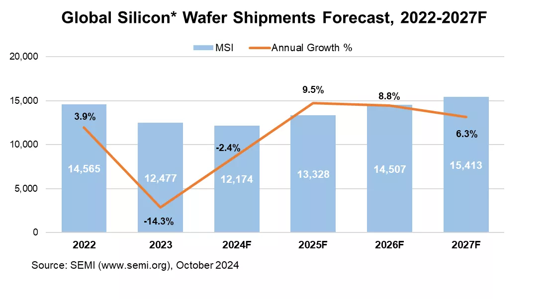
MILPITAS, Calif. — October 21, 2024 ─ Global shipments of silicon wafers are projected to decline 2% in 2024 to 12,174 million square inches (MSI) with a strong rebound of 10% delayed until 2025 to reach 13,328 MSI as wafer demand continues to recover from the downcycle, SEMI reported today in its annual silicon shipment forecast. 


Strong silicon wafer shipment growth is expected to continue through 2027 to meet increasing demand related to AI and advanced processing, driving improved fab utilization rate for global semiconductor production capacity. Moreover, new applications in advanced packaging and high-bandwidth memory (HBM) production, which require additional wafers, are contributing to the rising need for silicon wafers. Such applications include temporary or permanent carrier wafers, interposers, device separation into chiplets, and memory/logic array separation. 
 

SEMI Global Silicon Wafer Shipments Forecast

*Total electronic grade silicon slices – excludes non-polished and reclaimed wafers; shipments are for semiconductor applications only and do not include solar applications


Silicon wafers are the fundamental building material for the majority of semiconductors, which are vital components of all electronic devices. The highly engineered thin disks, produced in diameters of up to 300 mm, serve as the substrate material on which most semiconductor devices, or chips, are fabricated.

All data cited in this release include polished silicon wafers and epitaxial silicon wafers shipped by wafer manufacturers to end users. The data does not include non-polished or reclaimed wafers.


The SEMI annual silicon shipment forecast is developed based on input from the members of the Silicon Manufacturers Group (SMG). The SMG is a sub-committee of the SEMI Electronic Materials Group (EMG) and is open to SEMI members involved in manufacturing polycrystalline silicon, monocrystalline silicon or silicon wafers (e.g., as cut, polished, epi). The SMG facilitates collective efforts on issues related to the silicon industry including the development of market information and statistics about the silicon and semiconductor industries.


For more information, please visit SEMI Worldwide Silicon Wafer Shipment Statistics, SEMI Market Data or contact [email protected].


About SEMI

SEMI® is the global industry association connecting over 3,000 member companies and 1.5 million professionals worldwide across the semiconductor and electronics design and manufacturing supply chain. We accelerate member collaboration on solutions to top industry challenges through Advocacy, Workforce Development, Sustainability, Supply Chain Management and other programs. Our SEMICON® expositions and events, technology communities, standards and market intelligence help advance our members’ business growth and innovations in design, devices, equipment, materials, services and software, enabling smarter, faster, more secure electronics. Visit www.semi.org, contact a regional office, and connect with SEMI on LinkedIn and X to learn more.


Association Contact
Samer Bahou/SEMI
Phone: 1.408.943.7870
Email: [email protected]


MUNICH, Germany ─ October 14, 2024 ─ Semiconductor industry experts will convene at SEMICON Europa 2024, November 12-15 at Messe München in Munich, to explore the latest trends and innovations in advanced packaging and fab management. The Advanced Packaging Conference (APC) and Fab Management Forum (FMF) at SEMICON Europa will each focus on driving sustainable solutions to meet the evolving demands of the semiconductor market. Co-located with electronica, SEMICON Europa is the region’s premier event connecting the entire electronics design and manufacturing supply chain. Registration is open for APC and FMF.

SEMICON Europa"Global collaboration across the semiconductor industry is essential for driving sustainable, exponential growth,” said Laith Altimime, president of SEMI Europe. ”SEMI Europe Advanced Packaging Conference and Fab Management Forum provide invaluable platforms for stakeholders to share insights and innovations, ensuring we leverage cutting-edge technologies and strategies that enhance performance while paving the way for a more sustainable future." 

Advanced Packaging Conference ─ 
Chiplets and Heterogenous Integration: The Next Frontier in Performance and Efficiency 

Demand for High Performance Computing (HPC) is increasing, driven by advancements in artificial intelligence and Large Language Models like ChatGPT. HPC’s expansion requires innovative solutions in chiplet design, heat dissipation, and power optimization. The upcoming APC will provide a platform to explore enhancing each of these developments, highlighting collaboration among academia, industry, and government.   

This year’s APC will focus on:

  • The Role of Chiplets in Enhancing Performance and Efficiency
  • Power Optimization Techniques for Next-Generation Applications
  • Advances in Miniaturization and Material Integration
  • Innovations in Heat Dissipation and Thermal Management
  • Collaborations Across Academia, Industry, and Government   

Speakers include experts from Amkor Technology, ASE Global, Atotech an MKS Brand, Besi, Chip Integration Technology Center (CITC), Comet Yxlon, EV Group (EVG), Evatec, GlobalFoundries, Guangdong Fenghua Semiconductor Technology, Henkel, IBM, Infineon Technologies, JCET, Koh Young Europe, QuantumDiamonds, RHP-Technology, RoodMicrotec, Robovision, STATS ChipPAC, and SUSS MicroTec.

The conference is sponsored by ASE Global, Atotech an MKS Brand, Comet Yxlon, IBM, Koh Young Europe and SUSS MicroTec.

Fab Management Forum ─
Driving Innovation: Competitive, Sustainable and Collaborative Strategies 

To meet its evolving demands, the semiconductor industry must adopt competitive, sustainable, and collaborative strategies that enhance fab efficiency and performance. Industry stakeholders can develop innovative solutions for a sustainable future by integrating cutting-edge technologies and fostering partnerships.  This year’s FMF will focus on:

  • Key Strategies in a Global Market Landscape
  • Advancing Smart Manufacturing Solutions
  • Europe's Environmental Transition: Stability to Sustainability
  • Next-Gen Core Technologies for Future Fabs

Speakers include experts from Algorismic, ams OSRAM, BMW Group, Comet Yxlon, Flexciton, Infineon Technologies, INFICON, imec, Kontron AIS, minds.ai, Robert Bosch Semiconductor Manufacturing, STMicroelectronics, Synopsys, Texas Instruments, Tokyo Electron Europe, Watlow, and X-Fab.

The forum is sponsored by Comet Yxlon, Flexciton, INFICON, Lynceus, Tokyo Electron Europe (TEL), and Watlow.

Other SEMICON Europa 2024 Highlights

  • CxO Summit: Top executives will share strategies for sustainable growth in Europe's semiconductor sector, focusing on navigating the evolving landscape through sustainability, supply chain resilience, and technological advancements.
  • III-V Summit – Integrated Photonics: This summit will examine the role of III-V compound semiconductors in advancing next-generation electronics, focusing on their impact on high-performance, energy-efficient devices in telecommunications, computing, and photonics.
  • ITF Chip into the Future - Powered by imec: This session will cover the EU Chips Act's implementation and impact on Europe's semiconductor ecosystem, highlighting collaborative research and innovations in chip design and manufacturing.
  • MEMS & Imaging Sensors Summit: This summit will explore recent advancements in MEMS and imaging sensor technologies, focusing on their impact on agriculture, automotive, and healthcare, along with the integration of AI, machine learning, and data fusion in next-generation applications.
  • Executive Forum Programs: These sessions will provide updates on key technological trends, including Silicon Carbide (SiC) power semiconductors, smart mobility solutions, and AI-driven manufacturing processes. Industry experts will also address sustainable energy and challenges related to electrification, presenting the latest innovations aimed at overcoming these obstacles.
  • TechARENA Programs: Focused on emerging technologies, TechARENA sessions will explore advancements in fields such as medical technology, quantum computing, and cybersecurity. The discussions will also address global challenges related to supply chain management, sustainability, and talent development, with an emphasis on the role of European research and innovation in driving the growth of the semiconductor industry.

Programs in halls C1, C2 and Entrance West are complimentary for all SEMICON Europa and electronica visitors. For more details, please visit the SEMICON Europa 2024 website and connect with SEMI Europe on LinkedIn or X @SEMIEurope (#SEMICONEuropa).

SEMICON Europa 2024 

About SEMI 

SEMI ® is the global industry association connecting over 3,000 member companies and 1.5 million professionals worldwide across the semiconductor and electronics design and manufacturing supply chain. We accelerate member collaboration on solutions to top industry challenges through Advocacy, Workforce Development, Sustainability, Supply Chain Management and other programs. Our SEMICON ® expositions and events, technology communities, standards and market intelligence help advance our members’ business growth and innovations in design, devices, equipment, materials, services and software, enabling smarter, faster, more secure electronics. Visit www.semi.org, contact a regional office, and connect with SEMI on LinkedIn and X to learn more.

Association Contacts 

Maria Daniela Perez / SEMI Europe
Phone: +49 160 2562977 
Email:  [email protected] 

Samer Bahou / SEMI Corporate
Phone: +1 408 943 7870
Email: [email protected]

MILPITAS, Calif. – October 15, 2024 – SEMI, the global industry association representing the semiconductor and electronics design and manufacturing supply chain, today released a report by its Energy Collaborative(EC) with recommendations on expanding low-carbon energy (LCE) availability in Taiwan. The report explores existing Taiwan energy policies and offers solutions to address the market’s unique LCE procurement challenges. The EC report series on LCE availability includes recommendations for Japan and South Korea.

SEMI LogoAccording to the Semiconductor Climate Consortium (SCC), substantially scaling LCE investment and installation offers the most effective path for the industry to address customer expectations and pursue decarbonization targets. EC analysis suggests that more diverse procurement mechanisms and a higher level of cost-competitive LCE supply is required to prevent Taiwan’s corporate energy users from falling 30 to 50 percent short of their voluntary 2030 LCE adoption targets.

The EC has identified four key areas of LCE policy-related actions for Taiwan. Each recommendation is supported by detailed analysis of current and historical market conditions. In summary, the EC recommends:

  • Expanding procurement options by introducing mechanisms such as green tariffs and unbundled renewable energy certificates
  • Adjusting offshore wind localization requirements and, for offshore wind auctions, finding a balance with selection criteria such as cost, delivery timelines, and execution capabilities
  • De-risking power purchase agreements (PPAs) by redefining sell-back mechanisms for surplus electricity, especially for offshore wind
    • Evaluating effectiveness of offshore wind credit risk guarantees and consider extending the guarantee period
  • Alleviating land and community negotiation risks by enhancing the government’s role in land condition validation and creating guidelines on community benefit sharing.

“The EC welcomes recent energy policy developments in Taiwan that have gone into effect following our engagement meetings,” said Mousumi Bhat, vice president of Sustainability at SEMI. “We are encouraged by the revised auction rules designed to improve cost competitiveness and timely delivery. The EC and our members look forward to further engagement with developers, financiers and government agencies in support of this critical market for our industry.”

Other regional LCE policies reviewed in phase one of the SEMI Energy Collaborative Initiative include South Korea, Japan, Singapore and Malaysia, all key regions for semiconductor industry manufacturing. Each report leverages this comprehensive analysis and includes benchmarking information on how other regions have successfully implemented similar measures to drive LCE adoption.

The Energy Collaborative report Key Challenges and Potential Solutions for Expansion and Procurement of Low-Carbon Electricity on Taiwan is the third of five, joining the reports on South Korea and Japan. Organizations sponsoring the EC will get access to much more detailed analysis of each region. More information on the benefits of membership and sponsoring the Energy Collaborative initiative is available by contacting Jamie Belliveau at [email protected].

About the Energy Collaborative

The SEMI Energy Collaborative is dedicated to engaging a leadership network of corporations and domain experts to accelerate the pace of adoption of renewable energy solutions together with regional governments and regulators in key markets. Through collaboration with the semiconductor value chain, the EC aspires to improve the currently untenable trajectory of semiconductor manufacturing emissions. Companies sharing this vision from across the semiconductor and energy ecosystems sponsor the EC, along with partners from civil society and non-profit organizations.

About SEMI

SEMI ® is the global industry association connecting over 3,000 member companies and 1.5 million professionals worldwide across the semiconductor and electronics design and manufacturing supply chain. We accelerate member collaboration on solutions to top industry challenges through Advocacy, Workforce Development, Sustainability, Supply Chain Management and other programs. Our SEMICON ® expositions and events, technology communities, standards and market intelligence help advance our members’ business growth and innovations in design, devices, equipment, materials, services and software, enabling smarter, faster, more secure electronics. Visit www.semi.org, contact a regional office, and connect with SEMI on LinkedIn and X to learn more.

Association Contacts 
Samer Bahou/SEMI Corporate 
Phone: 1.408.943.7870 
Email: [email protected]

Elma Fang/ SEMI Taiwan
Phone: 886.3.560.1777
Email: [email protected]

MILPITAS, Calif. — October 7, 2024 — Electronic System Design (ESD) industry revenue increased 18.2% to $4,685.5 million in the second quarter of 2024 from the $3,962.7 million registered in the second quarter of 2023, the ESD Alliance, a SEMI Technology Community, announced today in its latest Electronic Design Market Data (EDMD) report. The four-quarter moving average, which compares the most recent four quarters to the prior four, rose 18%. 

SEMI & ESDA “The electronic design automation (EDA) industry reported substantial revenue growth in Q2 2024,” said Walden C. Rhines, Executive Sponsor of the SEMI Electronic Design Market Data report. “All product categories reported increases, with IC Physical and Semiconductor IP and Services posting double-digit growth. Further, all geographic regions reported double-digit growth.”


The companies tracked in the EDMD report employed 63,188 people globally in Q2 2024, a 6.8% jump over the Q2 2023 headcount of 59,160 and up 2.5% compared to Q1 2024.

The quarterly EDMD report contains detailed revenue information with the following category and geographic breakdowns.

Revenue by Product and Application Category – Q2 2024 Year-Over-Year Change 

  • Computer-Aided Engineering (CAE) revenue increased 8.9% to $1,646.4 million in Q2 2024. The four-quarter CAE moving average increased 16%.
  • IC Physical Design and Verification revenue grew 13.1% to $779.3 million. The four-quarter moving average for the category increased 17.1%.
  • Printed Circuit Board and Multi-Chip Module (PCB and MCM) revenue rose 8.2% to $399.2 million. The four-quarter moving average for PCB and MCM rose 13.6%.
  • Semiconductor Intellectual Property (SIP) revenue jumped 33.9% to $1,680.7 million. The four-quarter SIP moving average rose 21.7%.
  • Services revenue rose 30.8% to $179.8 million. The four-quarter Services moving average rose 18.4%.

Revenue by Region – Q2 2024 Year-Over-Year Change

  • The Americas, the largest reporting region by revenue, procured $2,034.9 million of electronic system design products and services in Q2 2024, a 25% increase. The four-quarter moving average for the Americas rose 18.3%.
  • Europe, Middle East, and Africa (EMEA) procured $584.6 million of electronic system design products and services, a 14.8% increase. The four-quarter moving average for EMEA grew 16.3%.
  • Japan’s procurement of electronic system design products and services grew 26.4% to $305.4 million. The four-quarter moving average for Japan increased 16.5%.
  • Asia Pacific (APAC) procured $1760.6 million of electronic system design products and services, an 11.2% increase. The four-quarter moving average for APAC grew 18.5%.

About the EDMD Report

The ESD Alliance Electronic Design Market Data report presents Electronic Design Automation (EDA), SIP and Services industry revenue data quarterly. Both public and private companies contribute data to the report available from SEMI. Each quarterly report is published approximately three months after quarter close. EDMD report data is segmented as follows:

  • Revenue by product category (CAE, IC Physical Design and Verification, SIP, PCB/MCM Layout, and Services) including numerous detailed sub-categories
  • Revenue by geographic region (Americas, EMEA, Japan and APAC)
  • Total employment at participating companies

For information about SEMI market research reports, visit the SEMI Market Research Reports and Databases Catalog.

About the Electronic System Design Alliance

The Electronic System Design (ESD) Alliance, a SEMI Technology Community, is the central voice to communicate and promote the value of the semiconductor design ecosystem as a vital component of the global electronics industry. As an international association of companies providing goods and services throughout the semiconductor design ecosystem, it is a forum to address technical, marketing, economic and legislative issues affecting the entire industry. For more information about the ESD Alliance, visit http://esd-alliance.org.

About SEMI 

SEMI ® is the global industry association connecting over 3,000 member companies and 1.5 million professionals worldwide across the semiconductor and electronics design and manufacturing supply chain. We accelerate member collaboration on solutions to top industry challenges through Advocacy, Workforce Development, Sustainability, Supply Chain Management and other programs. Our SEMICON ® expositions and events, technology communities, standards and market intelligence help advance our members’ business growth and innovations in design, devices, equipment, materials, services and software, enabling smarter, faster, more secure electronics. Visit www.semi.org, contact a regional office, and connect with SEMI on LinkedIn and X to learn more.

The information supplied by the ESD Alliance is believed to be accurate and reliable, but the ESD Alliance assumes no responsibility for any errors that may appear in this document. All trademarks and registered trademarks are the property of their respective owners. 

Association Contacts

Paul Cohen
Phone: 978-769-2106 
Email: [email protected] 

Jack Taylor
Phone: 512-560-7143 
Email: [email protected]

New Report from SEMI, TECHCET and TechSearch International Highlights Growth Drivers through 2028

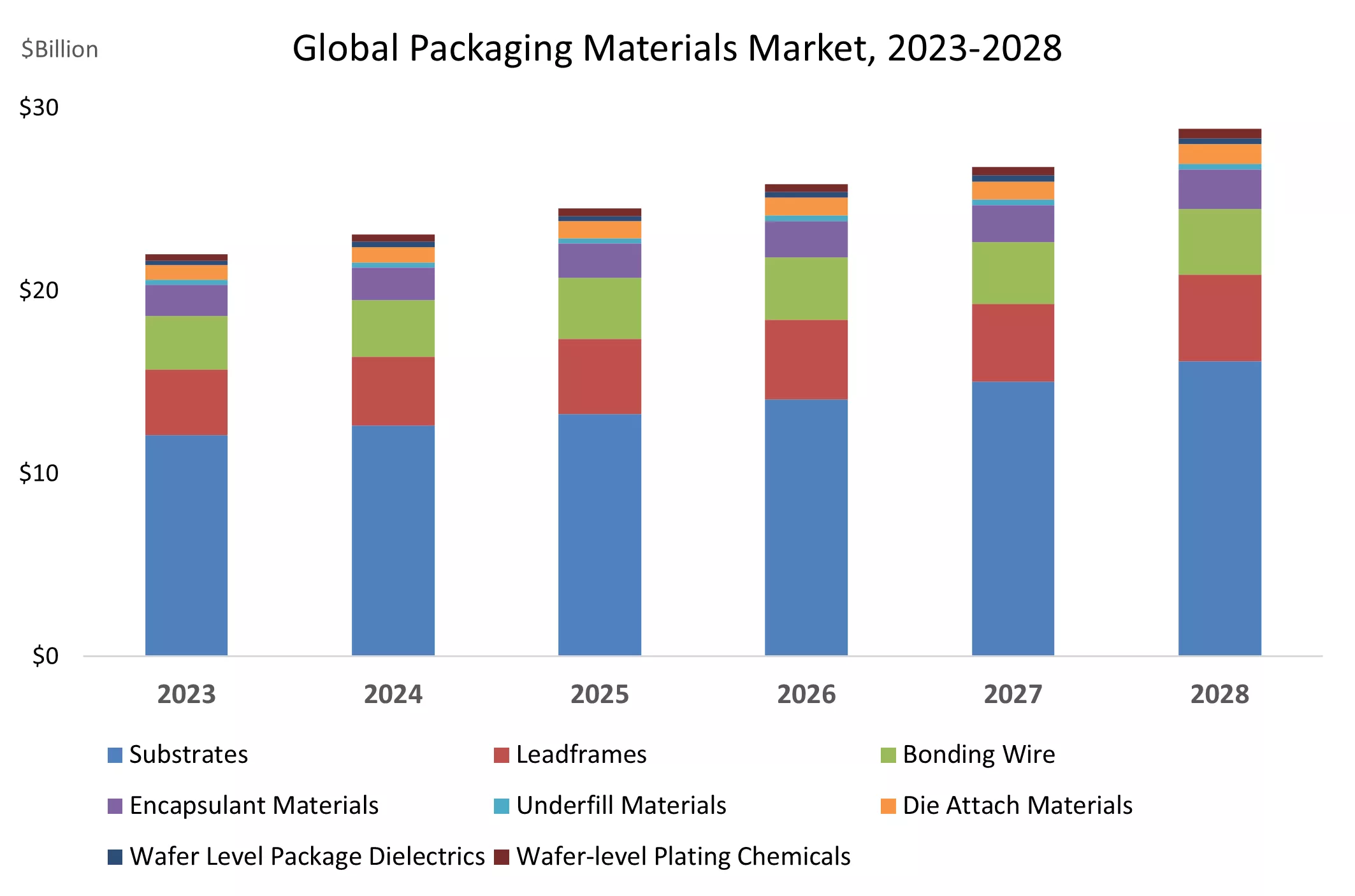
MILPITAS, Calif. — October 1, 2024 — Powered by strong semiconductor demand across diverse end applications, the global semiconductor packaging materials market is expected to start a growth cycle with a 5.6% compound annual growth rate (CAGR) projected through 2028, SEMI, TECHCET and TechSearch International announced today in their latest Global Semiconductor Packaging Materials Outlook (GSPMO) report. The report highlights AI as an expected growth driver for advanced packaging applications, despite currently low unit volumes due to the newness of the market segment.

Logos


The GSPMO report provides comprehensive data and forecasts for substrates, leadframes, bonding wire, and additional advanced packaging materials.

“After a challenging 2023, which saw a 15.5% decline in the semiconductor packaging materials market, our latest report forecasts a return to growth in 2024,” said Lita Shon-Roy, TECHCET President and CEO. “The global packaging materials market is expected to exceed $26 billion by 2025 and continue solid growth through 2028.” 

Global packaging materials


“Substrates account for a large portion of the revenue for the packaging materials market, and within the category, FC-BGA substrates make up the majority of the revenue growth,” said Jan Vardaman, President of TechSearch International. “The CAGR for flip chip BGA/LGA revenue is expected to be 7.6% from 2023 to 2028. Other key growth areas include wafer-level packaging (WLP) dielectrics and flip chip underfill. The laminate substrates segment is expected to grow 7.3% annually in volume, while leadframes and bonding wire are also forecasted to recover, growing by 5.0% and 6.4%, respectively.”

The GSPMO 2024 report is designed to help companies capitalize on emerging trends, navigate supply chain challenges, and make informed decisions in sourcing high-performance materials.

Features of the report include:

  • Technology trends
  • Regional market size and forecast
  • Five-year market forecast to 2028
  • Market size by product segments in revenue and units
  • Excel workbook file summarizing market information 
  • Supplier information and market share

For more information on the report or to subscribe, visit SEMI Market Data or contact the SEMI Market Intelligence Team (MIT) at [email protected].

About SEMI

SEMI® is the global industry association connecting over 3,000 member companies and 1.5 million professionals worldwide across the semiconductor and electronics design and manufacturing supply chain. We accelerate member collaboration on solutions to top industry challenges through Advocacy, Workforce Development, Sustainability, Supply Chain Management and other programs. Our SEMICON® expositions and events, technology communities, standards and market intelligence help advance our members’ business growth and innovations in design, devices, equipment, materials, services and software, enabling smarter, faster, more secure electronics. Visit www.semi.org, contact a regional office, and connect with SEMI on LinkedIn and X to learn more.

Association Contacts

Samer Bahou/SEMI Communications
Phone: 1.408.943.7870
Email: [email protected]

MILPITAS, Calif. –– September 30, 2024 –– Seeking to strengthen the semiconductor industry’s resilience to cybersecurity threats, the global association SEMI today announced the creation of a strategic roadmap for cybersecurity implementation throughout the industry. The SEMI Semiconductor Manufacturing Cybersecurity Consortium (SMCC) has partnered with the National Institute of Standards and Technology (NIST) to develop a semiconductor manufacturing industry profile for NIST Cybersecurity Framework 2.0 (CSF 2.0) that will serve as the foundation for the aforementioned roadmap. NIST plans to publish the profile in mid-2025. 

SEMI & SMCCAccording to research by the Identity Theft Resource Center, cyberattacks rose by 72 percentage points in 2023 over the previous all-time high in 2021. As semiconductor factories become increasingly connected and autonomous, the industry must respond to the growing security vulnerabilities associated with this next level of digital reliance and align with broader government efforts to secure the building blocks of technologies vital to society. 

“Semiconductors are integral to both national security and the global economy – we need to do everything in our power to protect the industry,” said Cherilyn Pascoe, Director of the National Cybersecurity Center of Excellence (NCCoE) at NIST. “NIST is pleased to partner with SEMI SMCC for the development and adoption of a NIST Cybersecurity Framework 2.0 Profile for Semiconductor Manufacturing. This collaboration is important to identify and reduce cybersecurity challenges in semiconductor manufacturing.”

“It’s important to recognize and address the unique cybersecurity challenges facing the semiconductor industry,” said Jennifer Lynn, SMCC Working Group Chair and Semiconductor Cybersecurity Lead at IBM Research. “This community profile could allow us to better identify and execute a path forward.”

In support of the 2023 National Cybersecurity Strategy’s strategic objective to secure global supply chains for information, communications and operational technology products and services, the White House Office of the National Cyber Director (ONCD) included a Cybersecurity Framework Profile as part of initiative 5.5.5 in the National Cybersecurity Strategy Implementation Plan Version 2. SMCC recognized the need for a cybersecurity community profile specific to semiconductor manufacturing and worked with the federal government to develop one. 

“Unlike air, space, land, and sea, cyberspace is the only battle domain created entirely by human hands,” said Anjana Rajan, Assistant National Cyber Director for Technology Security at ONCD, during the Global Executive Cybersecurity Forum at SEMICON West 2024. “This means we have both the power and the responsibility to shape it. The future of cyberspace where defenders have an inherent advantage over attackers starts with preparation, and that preparation must begin with securing the building blocks.”

Prior to completion, the community profile will open for public review and commentary in accordance with NIST’s official process. The review period has yet to be announced. The community profile is part of a broader NIST strategy to further standardize cybersecurity protocols for the semiconductor sector, in line with profiles for other industries.

“With the committed resources and support from NIST to support SMCC working groups, we’ll be able to accelerate the development of this semiconductor manufacturing industry community profile creation,” said Brian Korn, Director for SMCC and Staff Technologist focused on Cybersecurity and Automation at Intel Foundry. 

SMCC will provide cybersecurity recommendations for semiconductor manufacturing equipment, information on implementation, and updates on the development of the community profile. For more information, visit the project webpage or contact [email protected].

SMCC working groups are engaged with the SEMI Standards program to create a standards-based approach supporting the semiconductor ecosystem by leveraging the program’s 50-year history of industry alignment. SMCC is currently working on developments to two cybersecurity standards:

  • E187: Specification for Cybersecurity of Fab Equipment
  • E188: Specification for Malware-Free Equipment Integration

About SMCC 

The Semiconductor Manufacturing Cybersecurity Consortium (SMCC) is a SEMI technology community founded in 2024 to develop and promote a standard based, semiconductor industry wide approach to improve cybersecurity and accelerate implementation of actionable solutions. The vision of SMCC is to strengthen cyber resilience and protection of the global semiconductor supply chain against evolving threats. SMCC’s reach extends all over the world and enables our members to connect and collaborate on specific cybersecurity issues and challenges affecting different regions. It focuses on important key topics and seeks to find solutions that will benefit the entire industry. 

About SEMI

SEMI® is the global industry association connecting over 3,000 member companies and 1.5 million professionals worldwide across the semiconductor and electronics design and manufacturing supply chain. We accelerate member collaboration on solutions to top industry challenges through Advocacy, Workforce Development, Sustainability, Supply Chain Management and other programs. Our SEMICON® expositions and events, technology communities, standards and market intelligence help advance our members’ business growth and innovations in design, devices, equipment, materials, services and software, enabling smarter, faster, more secure electronics. Visit  www.semi.org, contact a regional office, and connect with SEMI on LinkedIn and X to learn more. 

About NIST 

The National Institute of Standards and Technology (NIST) was founded in 1901 and is now part of the U.S. Department of Commerce. NIST is one of the nation's oldest physical science laboratories. Congress established the agency to remove a major challenge to U.S. industrial competitiveness at the time — a second-rate measurement infrastructure that lagged behind the capabilities of the United Kingdom, Germany and other economic rivals.  

 The National Cybersecurity Center of Excellence (NCCoE) under NIST is a collaborative hub where industry organizations, government agencies, and academic institutions work together to address businesses’ most pressing cybersecurity challenges. This public-private partnership enables the creation of practical cybersecurity solutions for specific industries or broad, cross-sector technology challenges. Working with technology partners—from Fortune 50 market leaders to smaller companies specializing in IT security— the NCCoE develops modular, easily adaptable example cybersecurity solutions demonstrating how to apply standards and best practices using commercially available technology. 

About ONCD

The Office of the National Cyber Director (ONCD) advises the President of the United States on cybersecurity policy and strategy. Established by Congress in 2021, ONCD is a component of the Executive Office of the President at the White House. The Office spearheaded the development of the President’s National Cybersecurity Strategy, which President Biden issued on March 2, 2023. ONCD coordinates a whole-of-government approach to implement the National Cybersecurity Strategy.

ONCD’s mission is to advance national security, economic prosperity, and technological innovation through cybersecurity policy leadership. In carrying out its directive, ONCD works closely with White House and interagency partners, as well as with all levels of government, America’s international allies and partners, non-profits, academia, and the private sector, to shape and coordinate federal cybersecurity policy. Guided by the President’s vision, as articulated in the National Cybersecurity Strategy, ONCD is working to create a more equitable, safe, and resilient interconnected world in which every American can thrive and prosper.

Association Contact 

Samer Bahou / SEMI 
Phone: 1.408.943.7870
Email: [email protected] 

MILPITAS, Calif. — September 26, 2024 — Global spending on 300mm fab equipment is expected to reach a record US$400 billion from 2025 to 2027, SEMI highlighted today in its quarterly 300mm Fab Outlook Report to 2027 report. The robust spending is being driven by the regionalization of semiconductor fabs and the increasing demand for artificial intelligence (AI) chips used in data centers and edge devices.

SEMI LogoWorldwide, 300mm fab equipment spending is projected to grow by 4% to US$99.3 billion in 2024, and further increase by 24% to US$123.2 billion in 2025, surpassing the US$100 billion level for the first time. Spending is forecast to experience 11% growth to US$136.2 billion in 2026 followed by a 3% increase to US$140.8 billion in 2027.
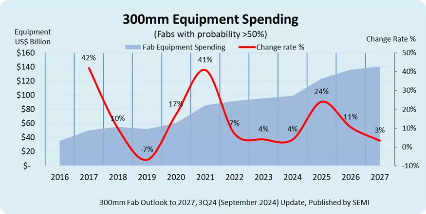
“The magnitude of the expected ramp of global 300mm fab equipment spending in 2025 sets the stage for a record-setting three-year period of semiconductor manufacturing investments,” said Ajit Manocha, SEMI President and CEO. “The world’s ubiquitous need for chips is boosting spending on equipment for both leading-edge technologies addressing AI applications and mature technologies driven by automotive and IoT applications.”


300mm Equipment Spending


Regional Growth

China is projected to maintain its position as the top spending region on 300mm equipment globally until 2027, investing over US$100 billion in the next three years driven by its national self-sufficiency policies. However, spending is anticipated to gradually decrease from a peak of US$45 billion in 2024 to US$31 billion by 2027.

Korea is projected to rank second and invest US$81 billion in the next three years to further its dominance in memory segments including DRAM, high-bandwidth memory (HBM), and 3D NAND Flash. Taiwan is forecast to spend US$75 billion on 300mm equipment over the next three years, ranking third as the region’s chipmakers build some new fabs overseas. Leading-edge logic below 3nm is the primary driver of Taiwan fab investments.

The Americas is projected to invest US$63 billion from 2025 to 2027, while Japan, Europe & Mideast, and SE Asia are expected to spend US$32 billion, US$27 billion, and US$13 billion, respectively, over the three-year period. Notably, these regions are anticipated to more than double their equipment investment in 2027 compared to 2024 due to policy incentives earmarked to alleviate concerns on the supply of crucial semiconductors.

Segment Growth

Foundry equipment spending is projected to reach approximately US$230 billion between 2025 and 2027, fueled by investments in sub-3nm cutting-edge nodes as well as continued spending on mature nodes. Investment in 2nm logic processes and development of key technologies at 2nm, such as gate-all-around (GAA) transistor structure and back-side power delivery technology, is crucial to meet future high-performance and energy-efficient computing needs, particularly for AI applications. Cost-effective 22nm and 28nm processes are expected to see growth due to increasing demand for automotive electronics and IoT applications.

The Logic and Micro segment is projected to spearhead the equipment spending expansion over the next three years, with an anticipated total investment of US$173 billion. Memory comes in second, expected to contribute over US$120 billion in spending during the same period, marking the beginning of another segment growth cycle. Within Memory, investment in DRAM-related equipment is projected to surpass US$75 billion, while investment in 3D NAND is expected to reach US$45 billion.

The Power-related segment ranks third, with an expected investment of over US$30 billion over the next three years, including around US$14 billion for compound semiconductor projects. The Analog and Mixed-signal segment is projected to reach US$23 billion during the same period followed by Opto/Sensors at US$12.8 billion.

Part of the SEMI Fab Forecast database, the SEMI 300mm Fab Outlook Report to 2027 report lists 420 facilities and lines globally, including 79 high-probability facilities expected to start operation during the four years beginning in 2024. The report reflects 169 updates and nine new fabs/lines projects since its last publication in June 2024.  

For more information on the report or to subscribe to SEMI market data, visit SEMI Market Data or contact the SEMI Market Intelligence Team (MIT) at [email protected].

About SEMI

SEMI® is the global industry association connecting over 3,000 member companies and 1.5 million professionals worldwide across the semiconductor and electronics design and manufacturing supply chain. We accelerate member collaboration on solutions to top industry challenges through Advocacy, Workforce Development, Sustainability, Supply Chain Management and other programs. Our SEMICON® expositions and events, technology communities, standards and market intelligence help advance our members’ business growth and innovations in design, devices, equipment, materials, services and software, enabling smarter, faster, more secure electronics. Visit www.semi.org, contact a regional office, and connect with SEMI on LinkedIn and X to learn more.

Association Contacts

Samer Bahou/SEMI Communications
Phone: 1.408.943.7870
Email: [email protected] 

Christian G. Dieseldorff/SEMI US
Phone: 1.408.943.7940
Email: [email protected]  

Chih-Wen Liu/SEMI Taiwan
Phone: 886.3.560.1777
Email: [email protected]