downloadGroupGroupnoun_press release_995423_000000 copyGroupnoun_Feed_96767_000000Group 19noun_pictures_1817522_000000Member company iconResource item iconStore item iconGroup 19Group 19noun_Photo_2085192_000000 Copynoun_presentation_2096081_000000Group 19Group Copy 7noun_webinar_692730_000000Path
Skip to main content
Default Banner Image

Artificial Intelligence

Outsourced Semiconductor Assembly and Test (OSAT) service providers experienced strong growth in 2017, but will this growth continue? In the last few years, OSAT growth has been driven by shipments for packages found in smartphones, but this market is slowing. What will replace it? Growth in power devices is strong and electronic content in vehicles is increasing. Will OSATs participate in this growth? Many OSATs have plants dedicated to automotive package assembly and will see continued growth. Growing demand for connectivity everywhere, called IoT, is generating large amounts of data, creating the need for more servers and datacenters. The adoption of Artificial Intelligence (AI) across a broad range of applications is driving demand for high-performance packages, but will this assembly take place at the OSATs or foundries? In the third and fourth quarters of 2017, growth in cryptocurrency provided unanticipated revenue for a number of OSATs. Given that the most well-known crypto mining companies and the biggest mining pools are all based in China, several OSATs, including major Taiwanese and Chinese service providers, experienced revenue growth in 2017 directly attributed to the assembly of ASICs in flip chip scale packages (FC-CSPs) and GPUs in flip chip ball grid arrays (FC-BGAs) for the cryptocurrency market. However, the first and second quarter of this year has seen decreased demand for GPUs and ASICs for this application. The assembly of packages for cryptocurrency slowed considerably in the first half of the year and therefore can’t be counted on to add as much to the revenue base as in the previous year. Going into the latter half of the year, the demand for Crypto ASICs is expected to pick up as new generation of 7nm chips will drive new investment and replacement cycle while crypto-mining GPU will see a further decline. Three of the top 10 OSATs, Jiangsu Changjiang Electronics Technology (JCET), Tianshui Huatian Technology (Huatian), and Tongfu Microelectronics (TFME), are based in China. China’s share of the top 10 OSATs’ revenue increased from slightly less than 23 percent in 2016 to more than 25 percent in 2017, and this trend is expected to continue. Crypto-related packaging and test business has certainly contributed a big portion of the share gain. Major OSATs such as TFME and Tianshui Huatian plan expansion in their plants and they expect to fill this added capacity in a broad range of packages. Huatian’s new Nanjing plant will include assembly for memory packages. TFME plans to set up a plant in Xiamen, Fujian Province to provide bumping, wafer level packaging, and system-in-packaging (SiP) services. Tracking the capabilities of OSATs is increasingly important. SEMI and TechSearch International have introduced a new Worldwide OSAT Manufacturing Site Database that provides listings of OSAT facility locations and package and test options in each factory. This database indicates the specific packages offered at each location. Finding plants that offer automotive qualified assembly is also possible with the database. Companies that offer bumping and wafer level packaging are identified. Over 120 companies and 300 facilities are tracked in this database covering both OSAT packaging and test facilities. For additional information about this informative database, please visit https://discover.semi.org/osat-database-registration.html E. Jan Vardaman is president of TechSearch International, Inc., and Clark Tseng is director of Industry Research and Statistics at SEMI.
Read More
SEMI FabView update for calendar year Q3 2018 Global fab construction investment shows continuing strength, with 19 new fab projects expected to begin construction in 2019 and 2020, based on the latest data published in SEMI’s World Fab Forecast. Fab investment is just one indicator of how growing demand in areas such as high-performance computing, data storage, artificial intelligence (AI), cloud computing, and automotive are driving the fourth consecutive year of spending growth in the semiconductor industry. Below are a few highlights* from September’s SEMI FabView: Memory: Not fading Micron plans to invest $3 billion by 2030 in Manassas, Virginia – These investments, driven by strong demand for automotive applications, are contemplated in Micron's long-term model. The production ramp is anticipated to be in the first half of 2020. SK Hynix to build new DRAM fab in Icheon (Gyeonggi Province), Korea – The construction, to be completed by the end of 2020, will adopt 1znm node (probably EUV). Total investment is estimated to exceed $13 billion. Nanya Technology doubles 2018 capex plan – The increase is for additional DRAM capacity and more 20nm DRAM conversion (from 30nm). 200mm and below: Not leading edge, but continues to draw investment Vanguard changes fab investment strategy – Vanguard will focus on 200 mm and has scrapped its plan for 300mm expansion. Murata to invest into 150mm expansion – Murata announced a 5 billion Yen investment (US$44.6 million) in a new fab extension in Vantaa, Finland. Investment, M A in Analog, Logic, Power and Opto Segments Texas Instruments is looking to invest $3.2 billion in new fab construction in 2019 – Texas Instruments is eyeing Richardson, Texas and also considering sites outside Texas. Bosch 300mm fab in Dresden, Germany – Bosch held a groundbreaking ceremony on April 24. Equipment installation is expected in 2H19. Microchip completes acquisition of Microsemi – Microchip closed its $8.45 billion acquisition of Microsemi on May 29. Microsemi has five fabs in the U.S. with a wide range of semiconductor products and system solutions. New fabs in China keep on coming Shanghai Jita Semiconductor/Huada Semiconductor – Shanghai Jita Semiconductor, a subsidiary of Huada Semiconductor and China Electronics Corporation (CEC), announced plans earlier this month to build both 200 mm and 300 mm semiconductor fabs for analog and power semiconductors in Shanghai. The combined fab investment will total $5.18 billion. Hamamatsu Photonics building 200 mm fab – Hamamatsu announced that it is building a new facility Investment of 2.8 billion Yen (US$25 million) to boost opto semiconductor capacity. Production is anticipated to start in late 2019. * Actual FabView updates provide more detail SEMI FabView, a mobile-friendly, interactive version of SEMI’s popular World Fab Forecast, delivers on-demand fab information such as fab spending and capacity for over 1,200 facilities, including over 60 planned facilities worldwide, across a wide range of product segments including Power, GPU, Memory, Foundry, MEMS and Sensors fabs. Fab data include region, start of construction, operation, construction and equipment spending, capacity, wafer sizes, product types and geometries. SEMI FabView subscribers receive forecast model updates through SEMI’s World Fab Database. Click here for a trial if you want to experience SEMI FabView first hand. Christian G. Dieseldorff is senior principal analyst and Eugenia Liu is senior product marketing manager, Industry Research and Statistics, SEMI, Milpitas, California.
Read More
SEMI Releases latest update to World Fab Forecast with adjusted semiconductor revenue consensus for second-half 2018 and 2019 Global semiconductor revenue in 2018 is now expected to reach $473.8 billion and clock a growth rate of 15 percent, a significant upward revision from the 7.5 percent expansion (to $442.9 billion) forecast at the start of the year by six research and investment forecasts tracked by SEMI Industry Research and Statistics (SEMI IR S). Data center growth will remain robust in the coming quarters, fueling demand for memory devices. In addition, cloud computing will continue to spur strong CPU, GPU, networking, ASIC, and DRAM and NAND demand through 2019, driving a consensus 3.63 percent year-to-year growth to reach the semiconductor revenue of $491 billion in 2019. Fab equipment spending (new and used) for 2018 is expected to increase by 14 percent to a record high of $63 billion, according to the last data from the SEMI World Fab Forecast, published by SEMI IR S. For 2019, fab equipment spending (new and used) is expected to increase 8 percent to another record of just under $68 billion. Memory continues to be the biggest swing factor in fab spending in 2018 and is expected to lead growth into 2020. 3D NAND will see the most capacity added in 2018 and 2019 with growth of 41 percent in 2018 and 27 percent in 2019, according to the SEMI World Fab Forecast. DRAM investment will see even stronger growth in 2018 and 2019 driven by new capacity addition as well as the continued technology shrink towards 1y/1z nm. For the first half of 2018, global spending for semiconductor fab equipment continues its growth momentum from 2017. Though we expect some softness in the second half of 2018, the outlook for 2019 remains robust with a fourth consecutive year of growth – the first such run since the 1990s. This prolonged growth cycle has been propelled by memory and will be extended by significant investment in China in 2019. Although a potential slowdown in 2020 is a concern, the overall outlook for semiconductor demand remains solid due to broad-based growth trends in data center, artificial intelligence (AI)/machine learning (ML), automotive, and industrial segments. Following are other SEMI forecasts for fab spending. Installed Capacity 3D NAND will see the most capacity added in both 2018 and 2019 with growth of 41 percent in 2018 and 27 percent in 2019. Foundry capacity growth is steady at 3 percent in 2018 and 6 percent in 2019, driven by both leading-edge and trailing-edge capacity buildup. 200mm fab capacity will increase 4 percent in 2018 and 3 percent in 2019, fueled by demand for MCU, sensors, PMIC, MOSFET and Driver IC. New Facilities / Construction Spending In 2018, there are 72 construction projects with investments totaling $15 billion, a year-over-year increase of 23 percent. Construction spending will reach all-time highs with China continuing its lead at US$7 billion in 2018, shattering its own record of $6.3 billion investment in 2017. Most construction spending in 2018 will be for Memory (just under $9 billion), primarily for 3D NAND followed by DRAM. Foundry will log second place in construction spending at just under $5 billion. Fab Equipment Spending Fab equipment spending (new and used) for 2018 is expected to jump 14 percent to a record high of US$63 billion, flat from the forecast issued in June 2018. Equipment spending (new and used) for 2019 is expected to increase 8 percent to another record of just under US$68 billion, a downward adjustment from +9 percent published in June 2018. We believe equipment spending will remain healthy, driven by solid, broad-based demand and predictable technology investments on top of constructive SEMICAP equipment fundamentals. Activity Report The August report features 1,265 records including about 300 Opto- and LED-related facilities. We have made 223 changes related to 216 fabs/lines. The modifications include the addition of new records, changes to existing records, the deletion of records since the February 2018 World Fab Forecast report. We are tracking 103 future facilities/lines with various probabilities that will start volume production in 2018 or later. Download a sample report Not a subscriber? Please review SEMI fab databases listed below. Our databases deliver the latest forecast and a complete analysis of front-end fabs and foundries worldwide. They are ideal resources to empower your market research. Eugenia Liu is a Senior Product Marketing Manager at SEMI.
Read More
Over the past three decades, most of the world’s innovations have centered largely on business models and involved iterative advances of existing technologies, with none matching the global impact of the top 10 semiconductor industry discoveries and advances, Dr. Morris Chang, founder of TSMC and the IC foundry model, said at SEMICON Taiwan 2018 this week.Few have as clear a perspective on the transformative power of semiconductors as Dr. Chang, founder of TSMC and father of the IC foundry model. Keynoting the IC60 Master Forum celebrating the 60th anniversary of the invention of the integrated circuit (IC), Dr. Chang listed what he considers the 10 key semiconductor industry innovation milestones since 1948:1. Invention of the transistor by Shockley, Bardeen, and Brattain – 19482. Silicon transistor – 19543. Integrated circuit – 19584. Moore’s Law – 19655. MOS technology MOS FET – 1964 Silicon gate – 1967 CMOS – 1970 6. Memory DRAM – 1966 Flash – 1967 7. Outsourced assembly and test (OSAT) – 1960s8. Microprocessor – 19709. VLSI systems design – 1970-1980 IP and design tools – 1980-present 10. Foundry model – 1985 Among the most consequential semiconductor advances may be yet to come, Dr. Chang said, citing innovations including artificial intelligence (AI) and machine learning, new device architectures, Extreme Ultraviolet lithography (EUV), 2.5D/3D packaging, and new materials such as graphene and carbon nanotubes.Dr. Chang argued that because bringing an innovation into production is immensely more expensive than proving a theory in a lab, innovators are not always the ones to implement and benefit from their novel ideas. Today, innovation costs are skyrocketing, driving more consolidation across the supply chain.Michael Droeger is director of marketing at SEMI.
Read More
2017 was a good year for the MEMS and sensors business, and that upward trend should continue. We forecast extended strong growth for the sensors and actuators market, reaching more than $100 billion in 2023 for a total of 185 billion units. Optical sensors, especially CMOS image sensors, will have the lion’s share with almost 40 percent of market value. MEMS will also play an important role in that growth: During 2018–2023, the MEMS market will experience 17.5 percent growth in value and 26.7 percent growth in units, with the consumer market accounting for more than 50 percent(1) share overall. Evolution of SensorsSensors were first developed and used for physical sensing: shock, pressure, then acceleration and rotation. Greater investment in R D spurred MEMS’ expansion from physical sensing to light management (e.g., micromirrors) and then to uncooled infrared sensing (e.g., microbolometers). From sensing light to sensing sound, MEMS microphones formed the next wave of MEMS development. MEMS and sensors are entering a new and exciting phase of evolution as they transcend human perception, progressing toward ultrasonic, infrared and hyperspectral sensing.Sensors can help us to compensate when our physical or emotional sensing is limited in some way. Higher-performance MEMS microphones are already helping the hearing-impaired. Researchers at Arizona State University are among those developing cochlear implants — featuring piezoelectric MEMS sensors — which may one day restore hearing to those with significant hearing loss. The visually impaired may take heart in knowing that researchers at Stanford University are collaborating on silicon retinal implants. Pixium Vision began clinical trials in humans in 2017 with its silicon retinal implants.It’s not science fiction to think that we will use future generations of sensors for emotion/empathy sensing. Augmenting our reality, such sensing could have many uses, perhaps even aiding the ability of people on the autism spectrum to more easily interpret the emotions of others.Through my years in the MEMS industry, I have identified three distinct eras in MEMS’ evolution: The “detection era” in the very first years, when we used simple sensors to detect a shock. The “measuring era” when sensors could not only sense and detect but also measure (e.g., a rotation). The “global-perception awareness era” when we increasingly use sensors to map the environment. We conduct 3D imaging with Lidar for autonomous vehicles. We monitor air quality using environmental sensors. We recognize gestures using accelerometers and/or ultrasonics. We implement biometry with fingerprint and facial recognition sensors. This is possible thanks to sensor fusion of multiple parameters, together with artificial intelligence. Numerous technological breakthroughs are responsible for this steady stream of advancements: new sensor design, new processes and materials, new integration approaches, new packaging, sensor fusion, and new detection principles.Global Awareness SensingThe era of global awareness sensing is upon us. We can either view global awareness as an extension of human sensing capabilities (e.g., adding infrared imaging to visible) or as beyond-human sensing capabilities (e.g., machines with superior environmental perception, such as Lidar in a robotic vehicle). Think about Professor X in Marvel’s universe, and you can imagine how human perception could evolve in the future! Some companies envisioned global awareness from the start. Movea (now part of TDK InvenSense), for example, began their development with inertial MEMS. Others implemented global awareness by combining optical sensors such as Lidar and night-vision sensors for robotic cars. A third contingent grouped environmental sensors (gas, particle, pressure, temperature) to check air quality. The newest entrant in this group, the particle sensor, could play an especially important role in air-quality sensing, particularly in wearable devices.Driven by increasing societal concern over mounting evidence of global air-quality deterioration, air pollution has become a major topic in our society. Studies show that there is no safe level of particulates. Instead, for every increase in concentration of PM10 or PM2.5 inhalable particles in the air, the lung cancer rate is rising proportionately. Combining a particle sensor with a mapping application in a wearable could allow us to identify the locations of the most polluted urban zones.The Need for Artificial Intelligence To realize global awareness, we also need artificial intelligence (AI), but first, we have challenges to solve. Activity tracking, for example, requires accurate live classification of AI data. Relegating all AI processing to a main processor, however, would consume significant CPU resources, reducing available processing power. Likewise, storing all AI data on the device would push up storage costs. To marry AI with MEMS, we must do the following: Decouple feature processing from the execution of the classification engine to a more powerful external processor. Reduce storage and processing demands by deploying only the features required for accurate activity recognition. Install low-power MEMS sensors that can incorporate data from multiple sensors (sensor fusion) and enable pre-processing for always-on execution. Retrain the model with system-supported data that can accurately identify the user’s activities. There are two ways to add AI and software in mobile and automotive applications. The first is a centralized approach, where sensor data is processed in the auxiliary power unit (APU) that contains the software. The second is a decentralized approach, where the sensor chip is localized in the same package, close to the software and the AI (in the DSP for a CMOS image sensor, for example). Whatever the approach, MEMS and sensors manufacturers need to understand AI, although they are unlikely to gain much value at the sensor-chip level.Heading to an Augmented WorldWe have achieved massive progress in sensor development over the years and are now reaching the point when sensors can mimic or augment most of our perception: vision, hearing, touch, smell and even emotion/empathy as well as some aesthetic senses. We should realize that humans are not the only ones to benefit from these developments. Enhanced perception will also allow robots to help us in our daily lives (through smart transportation, better medical care, contextually aware environments and more). We need to couple smart sensors’ development with AI to further enhance our experiences with the people, places and things in our lives.About the authorWith almost 20 years’ experience in MEMS, sensors and photonics applications, markets, and technology analyses, Dr. Eric Mounier provides in-depth industry insight into current and future trends. As a Principal Analyst, Technology Markets, MEMS Photonics, in the Photonics, Sensing Display Division, he contributes daily to the development of MEMS and photonics activities at Yole Développement (Yole). He is involved with a large collection of market and technology reports, as well as multiple custom consulting projects: business strategy, identification of investment or acquisition targets, due diligence (buy/sell side), market and technology analyses, cost modeling, and technology scouting, etc.Previously, Mounier held R D and marketing positions at CEA Leti (France). He has spoken in numerous international conferences and has authored or co-authored more than 100 papers. Mounier has a Semiconductor Engineering Degree and a PhD in Optoelectronics from the National Polytechnic Institute of Grenoble (France).Mounier is a featured speaker at SEMI-MSIG European MEMS Sensors Summit, September 20, 2018 in Grenoble, France. (1) Source: Status of the MEMS Industry report, Yole Développement, 2018
Read More
The march to greater precision, efficiency and safety – the lifeblood of high-technology manufacturing facilities – has taken on a new urgency as emerging applications such artificial intelligence (AI), the Internet of Things (IoT) and Industry 4.0 give new meaning to smart factories. Facing fiercer competition and ever more sophisticated fabrication processes, semiconductor fabs are under intense pressure to keep pace with new technologies as they work to upgrade. Nowhere are the stakes higher than in Taiwan, where high-tech manufacturing contributes mightily to the region’s GDP growth. To help Taiwan fabs confront the challenges and opportunities of designing smarter factories, SEMI and its High-Tech Facility Committee hosted the High-Tech Facility Workshop in June. SEMICON Taiwan 2018 High-Tech Facility Pavilion exhibitors gathered to explore how they can build smarter factories by deploying smart surveillance and disaster prevention technologies along with smart communications systems that better use manufacturing data to drive new safety and product quality efficiencies.During the workshop, SEMI High-Tech Facility Committee representatives shared strides it has made upgrading overseas facilities and developing standards to help establish smart factories in Taiwan.SEMICON Taiwan – 5-7 September at Taipei’s Nangang Exhibition Center – is also an important event for advancing smart manufacturing in Taiwan. Nearly 30 leading global manufacturers will exhibit at the SEMICON Taiwan High-Tech Facility Pavilion. The venue covers operational aspects of semiconductor manufacturing vital to becoming smarter including energy savings, nano-contamination control, facility information modeling, precision instrumentation and control, fire protection, mechatronics, and automation control. The pavilion will also feature a series of theme events offering a comprehensive overview of topics including the latest practices for integrating smart facility capabilities from the perspective of an advanced fab designer.At the TechXPOT stage, High-Tech Facility Pavilion exhibitors will also demonstrate the latest technology breakthroughs and cutting-edge smart factor solutions.The September 6th High-Tech Facility International Forum at SEMICON Taiwan will again gather factory experts and thought leaders from industry and academia to examine “Effective Ways to Make a Facility Smart.“ Experts from industry heavyweights in the fields of wafer foundry, LCD, memory and semiconductor packaging including TSMC, UMC, Innolux, ASE, Micron Taiwan, Winbond and VIS will offer insights into key areas of high-tech facilities including facility electricity, machinery, water management, vaporization and automation systems. On the same day as the forum, the High-Tech Facility Get-Together and High-Tech Facility VIP Dinner will bring together industry elites, academic professionals, and government officials to explore partnership opportunities. SEMI Taiwan and the High-Tech Facility Committee share HTF market trends information, technology updates and standards with SEMI members and exhibitors. Founded in 2013, the High-Tech Facility Committee now has 85 corporate members. Dedicated to accelerating industry collaboration through the integration of Taiwan industrial, government and academic resources, the committee each year holds several group meetings focusing on topics including energy savings, earthquake and fire protection, nano-contamination control, and precision instrumentation and control to advance critical technologies and facilitate standardization. The committee also aims to help the industry become more competitive faster by promoting technology standards that boost productivity and reduce production costs.Please visit www.semi.org and www.semicontaiwan.org for more information about SEMI’s high-tech facility initiatives.Iris Tsou is a marketing specialist at SEMI Taiwan.
Read More
Standing-room only keynote speeches. A future awash in data amassed by transformative technologies and applications, with semiconductors at their core. Smart everything: Cars, medicine, manufacturing, workforce, you name it. The sheer numbers impressed as a record lineup of SEMICON West keynote speakers offered a glowing portrait of the future: The semiconductor industry stands on the cusp of a breakout expansion. Standing and seated shoulder-to-shoulder in the packed-to-gills opening keynote, the audience learned, indeed, that the best was yet to come: “This is the best SEMICON West, ever,” observed SEMI CEO Ajit Manocha. Here’s a glimpse of the keynotes by the numbers, starting with the luckiest of all. 7 – The number of keynotes – among the brightest lights in technology – sharing their visions of the future through the lens of breakthrough technologies that are nearly ready to make their indelible mark. Dozens of expert panelists also weighed in at SEMICON West, the annual U.S. flagship microelectronics gathering in San Francisco. 90 – The percentage of all data ever generated has been created in just the past two years as the cloud mushrooms with tweets, texts, emails, Facebook posts, YouTube videos, medical records and all manner of business information, noted Bill Bottoms, president and CEO of Third Millennium Test Solutions. In the years ahead, an almost unimaginable wealth of data will require analysis by artificial intelligence (AI) embedded in semiconductors to enable applications that go well beyond smart. 12-18 – That’s how many months it will take for data volume to double, predicted John Kelly III, IBM’s Senior VP, Cognitive Solutions. And it will double again and again, every 12-18 months. Kelly foresees a scale of growth “that will dwarf previous eras of computing … the number of opportunities is enormous.” Kelly’s four decades in computing gave considerable weight to his point that “in the industry, there has never been a more exciting point in time than today.” First – Technology is being re-born. Using baseball lingo, several speakers noted that we are just in “the first inning,” “the top half of the first inning” or “the beginning of the first inning” to make clear in the most emphatic terms the duration of prosperity that lies ahead for the industry. AI embedded in chips and demand for real-time analysis of AI data will be its fuel. As SEMI Americas president Dave Anderson observed with a smile, “We all know how long baseball games can go.” Third – That’s the current wave of machine learning the world is now experiencing, according to Sandia National Laboratories’ Principal Member Conrad James. Computers are now capable of solving many increasingly complex problems on their own, with no human intervention necessarily required, he said. 1000x – As spectacularly fast as computing power already is today, the industry will need to double that the rate of performance in the years ahead, predicted Applied Materials president and CEO Gary Dickerson. Demand for this herculean processing capacity will spur a “tremendous focus on innovation” among SEMI members, their customers and their customers’ customers. 5 to 15 – The remarkable amount of silicon that power today’s mobile devices will be overshadowed by the chips – equivalent in computing capacity to 5 to 15 cell phones – that will be the engine of self-driving and other features in future automobiles, predicted Pierre Ferragu, New Street Research Managing Partner, during the SEMI Bulls and Bears session. Automobiles with this souped-up computing capacity will sell in the millions worldwide in the years ahead, generating never-before-seen opportunities for the chip industry, he noted. 10,000 – It’s not just cars. Ten thousand is the number of sensors that will be built just into the wings of new Airbus A380-1000 aircraft, AMD CTO Mark Papermaster explained during his keynote. 10 terabits – The staggering amount of Facebook data uploaded daily in to the cloud, Papermaster noted. 1 Trillion – SEMI’s 2020 forecast that the industry will reach $500 billion in revenues by 2020 was eclipsed by one analyst, speaking at the SEMI Market Symposium on the first day of the event, predicted that the industry would top $1 trillion in the foreseeable future. SEMI’s Manocha later added that $1 trillion in industry revenue is possible by 2030, “maybe sooner.” 1 (sexy) coda – Coders are hip and software applications are the apple of the world’s eye. Even the most casual mobile device user knows that software apps makes it whirl. But “hardware is becoming sexy again,” said Applied Materials’ Dickerson, adding that equipment and other semiconductor hardware developed by SEMI members will enable the next great wave of global economic growth. Scott Stevens, SEMI
Read More
With artificial intelligence (AI) rapidly evolving, look for applications like voice recognition and image recognition to get more efficient, more affordable, and far more common in a variety of products over the next few years. This growth in applications will drive demand for new architectures that deliver the higher performance and lower power consumption required for widespread AI adoption. “The challenge for AI at the edge is to optimize the whole system-on-a-chip architecture and its components, all the way to semiconductor technology IP blocks, to process complex AI workloads quickly and at low power,” says Qualcomm Technologies Senior Director of Engineering Evgeni Gousev, who will provide an update on the progress of AI at the edge in a Data and AI program at SEMICON West, July 10-12 in San Francisco. Qualcomm Snapdragon 845 uses heterogeneous computing across the CPU, GPU, and DSP for power-efficient processing for constantly evolving AI models. Source: QualcommA system approach that optimizes across hardware, software, and algorithms is necessary to deliver the ultra-low power – to a sub 1-milliwatt level, low enough to enable always-on machine vision processing – for the usually energy-intensive AI computing. From the chip architecture perspective, processing AI workloads with the most appropriate engine, such as the CPU, GPU, and DSP with dedicated hardware acceleration, provides the best power efficiency – and flexibility for dealing with rapidly changing AI models and growing diversity of applications.“So far it’s been largely a brute force approach using conventional architectures and cloud-based infrastructure,” says Evgeni. “But we’re going to run out of brute force options, so future opportunities lie in developing innovative architectures, dedicated hardware, new algorithms, and new software. Innovation will be especially important for AI at the edge and applications requiring always-on functionality. Training is mostly in the cloud now, but in the near future it will start migrating to the device as the algorithms and hardware improve. AI at the edge will also remove some privacy concerns, an increasingly important issue for data collection and management.”Practical AI applications at the edge where resources are constrained run the gamut, spanning smartphones, drones, autonomous vehicles, virtual reality, augmented reality and smart home solutions such as connected cameras. “More AI on the edge will create a huge opportunity for the whole ecosystem – chip designers, semiconductor and device manufacturers, applications developers, and data and service providers. And it’s going to make a significant impact on the way we work, live, and interact with the world around us,” Evgeni said.Future generations of chips may need more disruptive systems-level change to handle high data volumes with low power A next-generation solution for handling the massive proliferation of AI data could be a nanotechnology system, such as the collaborative N3XT (Nano-Engineered Computing Systems Technology) project, led by H.S. Philip Wong and Subhasish Mitra at Stanford. “Even with next-generation scaling of transistors and new memory chips, the bottlenecks in moving data in and out of memory for processing will remain,” says Mitra, another speaker in the SEMICON West program. “The true benefits of nanotechnology will only come from new architectures enabled by nanosystems. One thing we are certain of is that massively more capable and more energy-efficient systems will be necessary for almost any future application, so we will need to think about system-level improvements.” Major improvement in handling high volumes of data with low high energy use will require system-level improvements, such as monolithic 3D integration of carbon nanotube transistors in the multi-campus N3XT chip research effort. Source: Stanford UniversityThat means carbon nanotube transistors for logic, high density non-volatile MRAM and ReRAM for memory, fine-grained monolithic 3D for integration, new architectures for computation immersed in memory, and new materials for heat removal. “The N3XT approach is key for the 1000X energy efficiency needed,” says Mitra.Researchers have demonstrated improvements in all these areas, including multiple hardware nanosystem prototypes targeting AI applications. The researchers have transferred multiple layers of as-grown carbon nanotubes to the target wafer to significantly improve CNT density and have also developed a low-power TiN/HfOx/Pt ReRAM. The low-temperature CNT and ReRAM processes enable multiple vertical layers to be grown on top of one another for ultra-dense and fine-grained monolithic 3D integration. Other speakers at the Data and AI TechXpot include Fram Akiki, VP Electronics, Siemens; Hariharan Ananthanarayanan, motion planning engineer, Osaro; and David Haynes, Sr. director, strategic marketing, Lam Research. See SEMICONWest.org.Paula Doe, SEMI
Read More
Part 2 of this two-part piece examines the potential benefits to be realized by pairing human Subject Matter Experts with smart silicon assistants, and what these new arrangements mean for semiconductor device manufacturing. Part 1 explores best-practice perspectives on collecting and utilizing smart data in industries outside semiconductor manufacturing, one of the important takeaways from the Smart Manufacturing panel discussion at SEMI ASMC 2018. So what does this observation (i.e. the field of medicine, in what seems at first glance a big data environment, is really just clusters and clusters of loose small data connected by the collective neural network of highly trained doctors and their colleagues) mean for semiconductor manufacturing? 
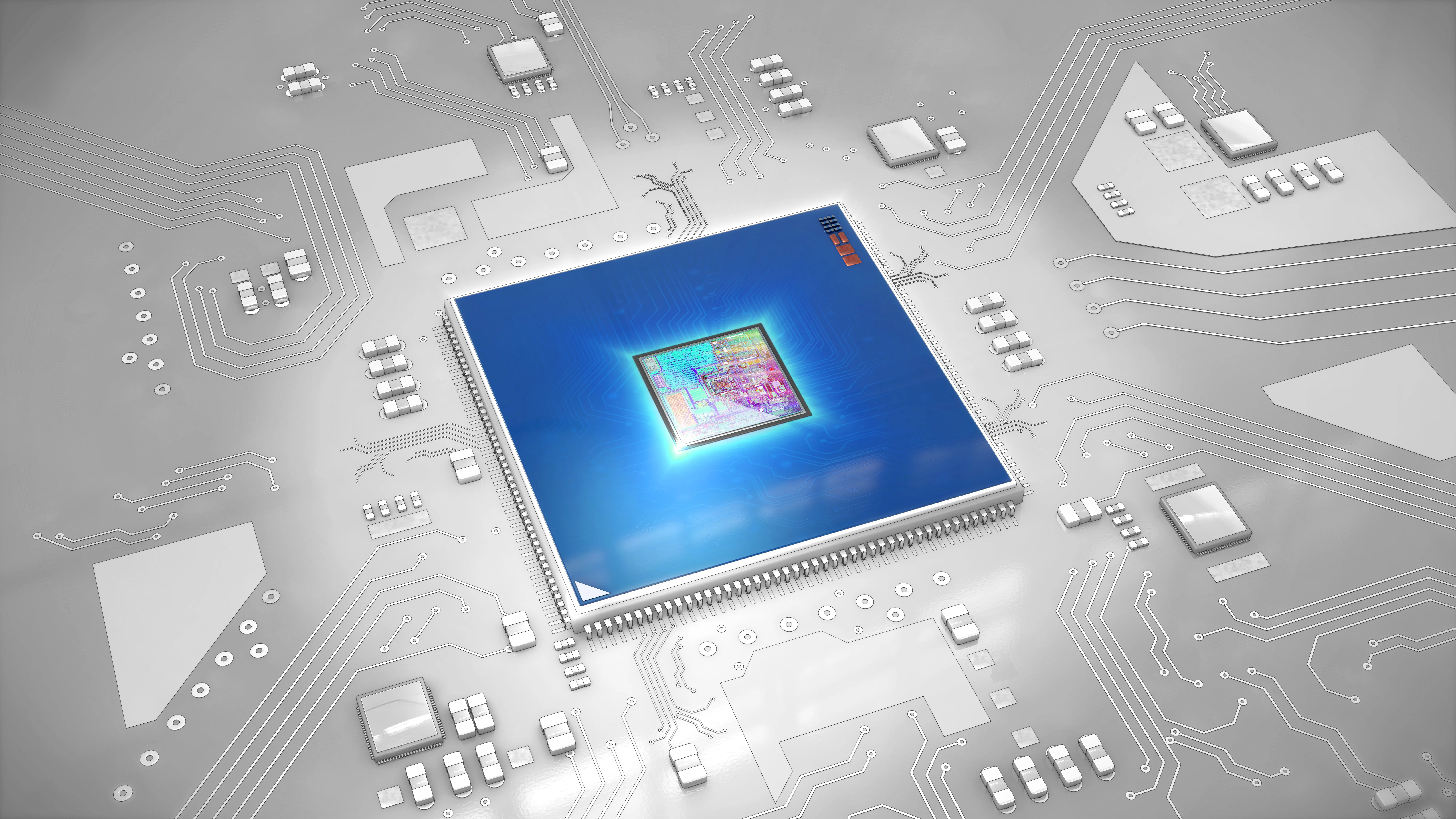
We think it means we need to apply the same level of intense focus that we already devote to instrumented data collection and analytics in the fab to something more: we need to better capture the vast expertise of our engineering and operational talent in semiconductor manufacturing. We think we need to record what the subject matter experts (SMEs) in the fab see, hear, and think as they investigate yield excursions or machine-down problems. We need to effectively combine product, process, equipment and component subject matter expertise / subject matter experts (SME) with big data analytics to more effectively solve manufacturing problems, be they killer or be they chronic. And we must provide structured methods for incorporating inputs from and active participation of SMEs throughout the data analysis lifecycle, from collection and aggregation, through filtering, feature extraction, analysis and optimization. 
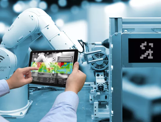
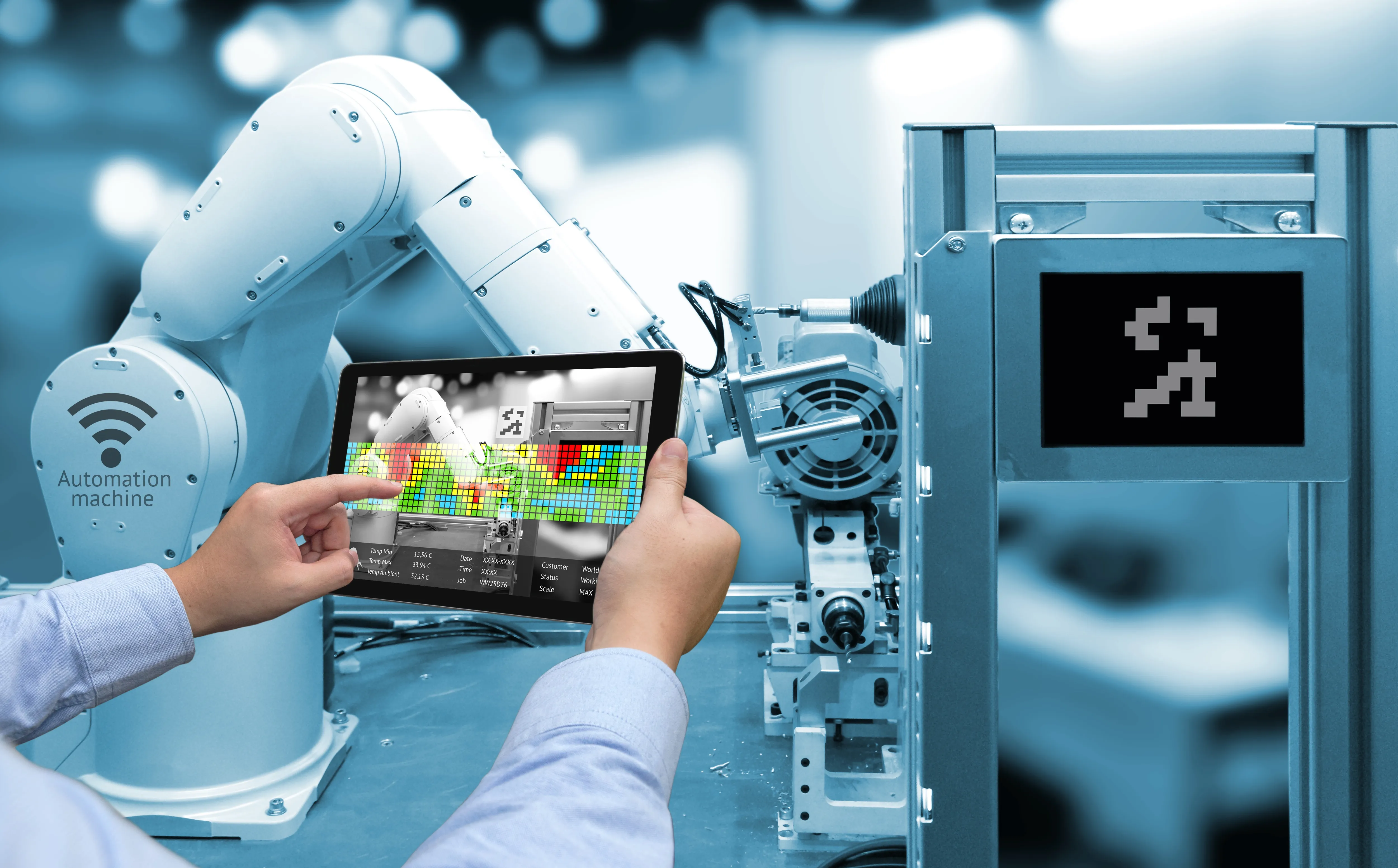
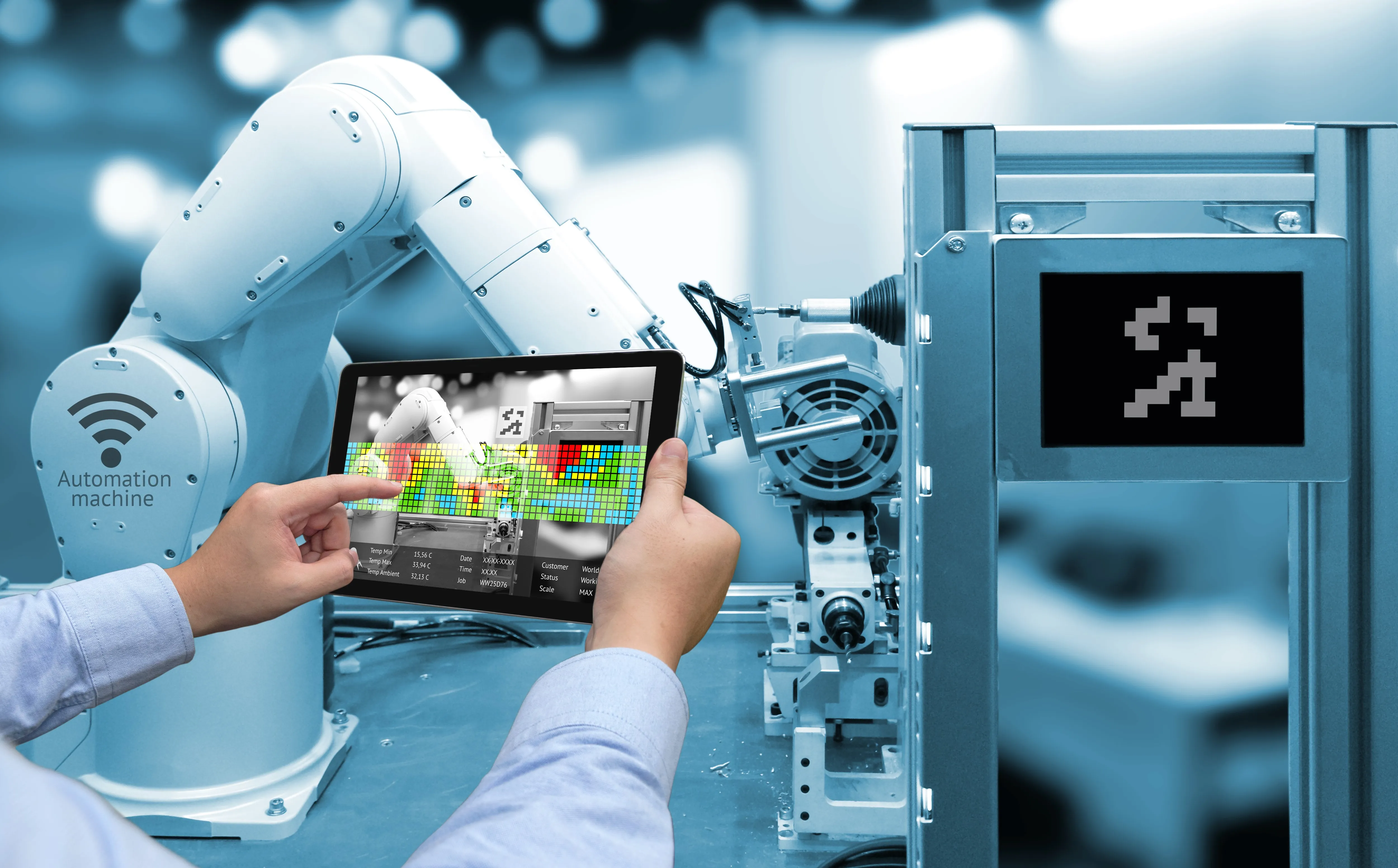
Some of the challenge will be in just how do we make it easy to gather information from SMEs in real time, while standing in front of equipment in the fab. Internet of Things (Iot) devices are emerging to capture and label images and sounds to enable machine learning algorithms to recognize and help diagnose manufacturing problems based on sight and sound, complementing the instrumented data. But we also need to record the thought processes our human SMEs go through in those investigations – perhaps by the SMEs talking to a smart AI-based conversational assistant who helps make “rounds.” Doing contextual analysis on this added data, combined with the instrumented data, will create the equation Human + Machine = AI (Awesome Insight). Sounds reasonable, right? We think artificial intelligence becomes too artificial if you leave the human out of the equation. AI should be augmented intelligence, where we take the expertise and creativity of the human, and combine it with the rapid computational capabilities of the computer, in order to put problem identification and solutions on steroids. But with the already huge advancements to date in data analytics, cloud, and the emergence of AI, why do improvements in quality, machine utilization, and the implementation of predictive analytics in semiconductor manufacturing seem to be creeping along incrementally, and not appearing as dramatic, step-function improvements? Call it Smart Manufacturing, call it Connected Enterprise, call it Advanced Manufacturing, or Analytics, or Cloud, or the Digital Twin … there are no shortages of terms, philosophies, and technologies available, but why aren’t we seeing their rapid adoption? It could be it’s the downside that comes with needing people. “Good business leaders create a vision, articulate the vision, passionately own the vision, and relentlessly drive it to completion.” Jack Welch. We see from other industries that smart manufacturing conversations originating with the executives of a company thinking to implement smart manufacturing programs lead to vision; however, we also see from other industries, and from our own, that realizing this vision has often been a challenge. Why is that? One reason may be that the people who are personally vested in solutions they implemented in the past, as well as those who follow a pattern of ‘how we’ve always done things’, create, inadvertently or not, persistent internal barriers hindering innovative action. Another may be that engagements with the working engineers and managers charged to be smart manufacturing implementers leads to the pursuit of low-hanging fruit, and cautious investments, that often utilize solutions that ultimately cannot scale and integrate. Not to mention the disadvantage of dealing with the legacy equipment, the legacy networks, the traditional thinking, and the lack of consistency in metrics adding to the confusion. Addressing all these barriers requires an alignment in strategy and execution, along with a plan to support the overall vision, often across the entire enterprise, which is no small matter. And then there are the standards. Having and adhering to standards in control solutions, networks, and data becomes critical in achieving real benefits from smart manufacturing. And data security. One of the other big impediments in the smart manufacturing transformation is data and IP security, another key concern (maybe the most significant) preventing us from moving forward more quickly (e.g. to cloud-based solutions) in our industry. More about that in a follow-up. Achieving synergy across all of manufacturing, from connecting equipment horizontally, through the production system (machines processes), and vertically, through enterprise systems and across production facilities, can only occur if we build standards, security, infrastructure, and human engagement throughout our ecosystem and supply chain. In simple form, the steps to do so include connecting assets, collecting and contextualizing data, and then driving business transformation with actionable insights gained from the data. With impact on every function, and every person, in the enterprise, from equipment operators in the fab through the C-Suite in HQ. Maintenance, Engineering, R D, Operations, Scheduling, IT, Procurement, Finance, HR all contribute, collaborate and benefit. Regardless of the technology, from device level analytics to predictive maintenance and optimization, the people that reside in these disparate groups need to come together with the smart machines to create a common strategy to achieve transformational results. Aligning an enterprise’s goals with its human capital is paramount to success. Therefore, we must challenge our team members and ourselves to work outside our comfort zones, and we need to be forever aware of the need for us to grow with the technology. Smart manufacturing is not necessarily about having fewer people in the fab, but it does suggest having people in the fab, perhaps with different, or upgraded, skill sets, who are even more efficient in their roles as a result of the boost they are getting from Industry 4.0. Fortunately, we now have techniques that let us combine the best, brightest, and latest and greatest analytics with our invaluable SMEs throughout the data analysis lifecycle. We’ll not only be able to deliver higher quality semiconductor manufacturing solutions all in all, but we’ll also be providing methods to more easily distribute, scale, maintain, and continually refine those hard-earned solutions. We expect that subject matter experts will continue to put the “smart” in machine-based smart manufacturing today, and for the foreseeable future. SME contributions are not an option, but, rather, an imperative for ensuring a semiconductor manufacturer’s sustained prosperity, much less its survival. Nancy Greco (IBM Watson), Dave Mayewski (Rockwell Automation), James Moyne (University of Michigan / Applied Materials), and Paul Werbaneth (Intevac, Inc.), along with Julie Jacob (Ernst Young), and Carson Henry (Micron Technology), were members of the SEMI ASMC 2018 panel discussing Industry 4.0 and the Future of Commercial Semiconductor Device Manufacturing. All opinions here are purely our own. Please contact Paul Werbaneth via email at [email protected]. The SEMICON West (July 9-11, 2018, in San Francisco) Smart Manufacturing Pavilion features working production equipment on the floor and three full days of speakers providing insights on building the infrastructure needed to enable AI. Equipment from Bosch Rexroth, Cimetrix, Rudolph Technologies, INFICON, Final Phase Systems, OMRON, DISCO and Edwards Vacuum will showcase cutting-edge smart manufacturing technologies. For information on the SEMI Smart Manufacturing initiative and how to get involved, please click here.
Read More