downloadGroupGroupnoun_press release_995423_000000 copyGroupnoun_Feed_96767_000000Group 19noun_pictures_1817522_000000Member company iconResource item iconStore item iconGroup 19Group 19noun_Photo_2085192_000000 Copynoun_presentation_2096081_000000Group 19Group Copy 7noun_webinar_692730_000000Path
Skip to main content
Default Banner Image

Artificial Intelligence

METIS, a Sector Skills Alliance project co-funded by the European Commission’s Erasmus+ Program and coordinated by SEMI, recently launched an online questionnaire aimed at gauging the skills and expertise the industry needs to drive continued growth over the next five years. The survey, which will stay online until 15 October 2020, is a part of the METIS project’s efforts to involve a broad range of stakeholders in the microelectronics industry to assess workforce, future technology and economic trends influencing talent development and the skills needed most today and in the next five years. The survey aims to highlight the skill mismatches in specific job profiles that are of increasing importance to the microelectronics industry. It elaborates on the upskilling and reskilling needs for design engineers. Given that semiconductor design is becoming increasingly crucial for Europe’s competitiveness and technological sovereignty, the new skills required from design engineers are a priority area for the METIS project. Other examples are the manufacturing and maintenance technicians, two job profiles that are currently experiencing significant shifts in their skillsets, as COVID-19 has thoroughly transformed their way of work.While the microelectronics industry has been very aware of the importance of the high level of investment in R D, it is equally crucial to ensure that the workforce of the industry is equipped with knowledge and skills for the rapid technological developments. Maintaining high levels of investment in workforce including attracting talent, updating their knowledge and skills with the latest technological development, and supporting them to lead innovations, is essential for this industry. There is a growing demand for specific requirements for this sector to support innovation in many other sectors such as automotive, energy, healthcare, and government, to foster benefits from emerging digital technologies such as Cloud Services, Internet of Things (IoT), Artificial Intelligence (AI), Digital Reality, and Blockchain.In addition to the online questionnaire, the METIS project consortium is interviewing top experts from leading microelectronics companies, education representatives from universities and training academies, and experts from government agencies and industry associations. The interview outcomes provide inputs on what kind of employee profiles are the most difficult to find, what skills this sector is looking for in a candidate, and what kind of training and policy frameworks are needed to improve employers’ skills. Those inputs are essential to develop the skill strategy and form recommendations on training modules.Furthermore, the METIS project consortium is organizing 10 focus groups. Each of the focus groups is dedicated to a key topic, such as SC design, SC materials, semiconductor manufacturing equipment, etc. For example, one of the METIS focus groups is dedicated to Edge AI, a top priority for the microelectronics industry. Strengthening the AI talent pipeline is essential to harness the potential of Edge AI in Europe and to facilitate the shift from the Cloud to the Edge when possible in order to meet specific demands (e.g. for autonomous driving), reduce energy consumption for data communications, and to increase efficiency. The EU’s White Paper “Artificial Intelligence - A European approach to excellence and trust”[1] , published this February, also emphasizes the importance of upskilling and reskilling to position Europe among the global leaders in AI. Hence, the focus group will work towards pinpointing the skills necessary for the semiconductor workforce to capture the potential of the trend.The results of the survey, interviews and focus groups will be used to form the Microelectronics Skills Strategy. Based on this strategy, the METIS project will design 43 training modules for 1,100 hours learning in four key areas of the microelectronics sector:Component designSystem designBasic of manufacturingKey competencies and innovative thinkingThe METIS project is planning to recruit 2,000 learners in companies and education and training institutes to participate in the trainings and validate the impact. The METIS project will also work with companies, education and training providers to ensure continuity of the initiative and foster cooperation.During the METIS project course (2019 – 2023), the Skills Strategy will be updated yearly to reflect the latest technology and market trends. To enable the Skills Strategy to continue serving the industry, METIS is working on forming a permanent instrument, named Observatory and Skills Council, to continue developing the skills strategy, update the training and facilitate cooperation between industry and education and training providers.Laith Altimime, president of SEMI Europe, and 50 members of the Microelectronics Training, Industry and Skills (METIS) consortium The METIS consortium invites companies and associations involved in microelectronics training and education provision, human resources and career services professionals, technology strategists and policy makers to complete the online questionnaire. Stakeholders are also welcome to subscribe to the METIS newsletter for the latest on METIS programs. For more details, please contact Yanying Li at [email protected].[1] EU’s White Paper on Artificial Intelligence available at: https://ec.europa.eu/info/sites/info/files/commission-white-paper-artificial-intelligence-feb2020_en.pdfDr. Yanying Li is senior manager of Collaborative Projects at SEMI Europe.
Read More
MEMS and image sensors are shining stars in the chip industry as technology companies worldwide accelerate innovation in the fight against COVID-19. The tiny devices are behind advances in areas of electronics ranging from thermal imaging and faster point-of-care testing to microfluidics-based polymerase chain reaction (PCR) tools and techniques to detect SARS-CoV-2.SEMI recently spoke with Yole Développement analysts Dimitrios Damianos and Chenmeijing Liang about MEMS and imaging sensors market trends and how microelectronics-enhanced technologies are supporting the worldwide push to contain the spread of COVID-19.For additional insights on the technologies, join the SEMI MEMS Imaging Sensors Summit, held for the first time at SEMICON Europa, 12-13 November 2020 in Munich, Germany. Registration is open.SEMI: Despite the global pandemic, the MEMS and sensors market is still growing and is one of the healthiest industries, not only in Europe, but globally. What is driving this growth?Damianos: MEMS have been continuously evolving from the first sensors that were measuring pressure and acceleration to rotation sensing and visible light management followed by light sensing beyond visible and the expansion to ultrasound and multi-spectral. Now we are heading towards an era where we want to sense every aspect of our environment, with more processing and eventually analytics bringing more quality to the data.COVID-19 has impacted various global markets in very different ways. While automotive, mobility and civil aviation have suffered, the impact on telecommunications and medical has been positive. The effects on the consumer, mobile and industrial markets have been moderate. Moreover, COVID-19 is changing the perception of the current global supply chain in manufacturing, potentially leading to more localized value chains and further regionalization in order to minimize similar risks posed by the pandemic and the first lockdown.SEMI: Who are the main MEMS players based on your research? Damianos: For MEMS players, the picture in 2019 was not the same as 10 years ago, when Texas Instruments (TI) and Hewlett-Packard (HP) were leading the scene, with Bosch and ST Microelectronics following, all at comparable revenue levels. Now, Broadcom and Bosch lead with almost $1.4 billion in revenue each, and the rest of the MEMS key stakeholders compete in the $400 million to $600 million league. Microphone players profited from the voice interface adoption trend, while players active in MEMS for mobility and smartphones suffered slightly due to weak end-system demand.SEMI: What scenarios can we expect for each market with regard to the impact of COVID-19 on MEMS for 2020? Damianos: For 2020, at Yole Développement we expect the consumer market to contract slightly by 2.6%, with the automotive market to dip by 27.5%, and defense and aerospace by 20.5%. For the defense market, no major effect is expected, as all major programs still run for the year. The market may experience some slight delays in deliveries due to supply chain and logistics problems. However, sensors integrated in commercial/civil aerospace applications will suffer due to the general paralysis of the air travel industry. On the positive side, telecommunications could increase by 4.7%, medical applications by 10.6%, and industrial by 11.5%.Due to the global pandemic, some types of MEMS have spiked in demand this year. For example, demand for thermopiles and microbolometers used in temperature guns and thermal cameras has increased because of the need for contactless monitoring of people’s temperatures. Moreover, microfluidics for DNA sequencing and real-time polymerase chain reaction (PCR) diagnostic tests for detecting COVID-19 are gaining market relevance, with the latter serving as a premier method of detecting a bacteria or virus on the molecular level with high degrees of accuracy. Furthermore, pressure and flowmeters in ventilators will grow because of huge demand by hospital intensive care units (ICUs).SEMI: What growth trends do you predict for the long haul?Damianos: In the longer term, we expect global MEMS volumes to almost double, from 24.4 billion units in 2019 to 50.8 billion units in 2025, with a 13% CAGR during the same period. The global MEMS market could reach $17.7 billion in revenue by 2025.We see a trend to more wearable devices integrating a lot of sensors but also a move to a more consumer-oriented healthcare. Moreover, everything related to voice interfaces and voice/virtual-personal assistants (VPAs) will continue to see strong growth, increasing demand for MEMS mics with better quality and high-fidelity voice capture. MEMS devices are shifting to higher accuracy, ultra-low power, embedded intelligence and possibly some bio-compatibility for medical applications.MEMS players will try to escape the commoditization cycle and deliver more value by increasing the value of the data, either grouping many sensors to create sensor hubs or by adding processing, algorithms and software. Industry players are employing strategies such as adding extra processing close to the sensor (e.g. Knowles) or ameliorating the use cases of their applications of their clients (e.g. Bosch or ST). AI on the edge seems very alluring for extra value acquisition, with many startups already working on it. Some examples include always-on-sensing (Aspinity in collaboration with Infineon, Syntiant), echolocation (IMERAI) and predictive maintenance using inertial sensors (Cartesiam). This will be the next pit stop for MEMS technology for sure. SEMI: The CMOS Image Sensor (CIS) is a cornerstone technology in the development of devices powered by machine sensing and artificial intelligence (AI) for applications such as advanced driver assistance system (ADAS). CIS powers many of the ongoing revolutions in new technical products and use cases. What is the status of the image sensors industry? Liang: Last year was exceptional with a combination of high demand and high prices due to capacity limitations. Q4 2019 went way above the forecast, and, in the end, the CIS industry reached $19.3 billion for the full year. This year, we think it will return to normal, and, despite the pandemic impact, we expect significant growth in the range of 7% to 12%. Last year’s 25% year-over-year (YOY) growth was the highest we’ve seen over the past decade. Mobile still dominates the marketplace for CIS with 69% market share. Two markets, computing (8%) and consumer (5%), are adjacent to the mobile market but progressively losing ground due to the smartphone disruption.Security, at 6% market share, will probably be the second largest CIS market in the future. Although this is an area of excellence for the emerging Chinese players, unfortunately, they could be hit by the current trade war. The automotive market did very well from 2018 to 2019 because of the numerous applications recently developed for ADAS, viewing, and in-cabin applications. Lastly, the industrial camera applications benefited from large investments in automation, especially in the semiconductor and automotive industries, but here again many uncertainties remain as these markets will reshuffle in the post COVID-19 world. SEMI: Which CIS markets are most susceptible to seasonality and the impact of COVID-19?Liang: According to our quarterly CIS monitor, automotive and security were both negatively impacted by the pandemic beyond what we expected in terms of seasonality. For computing, the situation improved just prior the lockdown. Q1 got a positive impact with high sales results for laptops and tablets, but no significant impact was seen for security equipment. For automotive, the demand for cameras was very high in Q1, which is seasonally normal, despite the decrease of car shipments that followed later. The automotive CIS market in 2020 should remain relatively flat compared to 2019 due to the higher attachment rates of cameras despite the lower number of cars produced. Consumer and industrial segments dropped in Q1, which is typical early in the year.The next five years might be a bit slow, and although we forecast growth for the next year, in the future the market share will be lower in mobile. In fact, mobile CIS growth will fall below the CIS growth average, but we will see an increase of market share for the security, automotive and industrial segments. The CIS market could reach $28 billion in 2025.At first, COVID-19 had a limited impact on the production side, as factories in China are usually closed for the New Year holiday, when the pandemic started. While supply is currently recovering, we still consider the limited impact on demand. Smartphone production for 2020 will be down 6%, but camera shipments for mobile should increase about 10% this year. Another positive trend for the mobile market is optical fingerprint implementation. Currently, high-end Android phones use this kind of technology. For 2023, we estimate optical fingerprint technology revenue to be over $1 billion.The roadmap for the automotive market is driven by camera proliferation. We’ll see 10 cameras per car and more for some high-end vehicles. Increasing demand for safety and convenience will mean more cameras per car in the future. With a strong attachment rate, the market average in automotive is around 2.0 cameras per car nowadays, and we expect the market average to reach 3.5 cameras per car in 2025. In security, Charge Coupled Device (CCD)-based cameras are nearly out of the market, as CMOS-based IP cameras are most important now.SEMI: What are current key technology trends?Liang: 3D semiconductor technology is the hot topic. CIS wafer staking technology is indeed at the center of the CIS technology race. Future applications could be AI analytics or recently developed applications on new types of CIS. So far, we have seen the introduction of variants of the CIS pixel. Global shutter (GS) and indirect Time of Flight (iToF) were recently introduced, and now direct time-of-flight (dTOF) pixels are being used in high volume. 3D semiconductor technology is a bonanza for the industry, as it allows to pack more value in a single chip. While the surface of silicon is still increasing, additional silicon is added through stacking.With COVID-19 still a problem, the endpoint for smartphones in 2020 remains uncertain. The short-term impact for CIS will be slower growth with respect to the 25% YoY of last year. The downturn in car production will be mitigated by an increased attachment rate for automotive cameras. The security market will also help maintain CIS growth.For more insights, see the following reports: Status of the MEMS Industry 2020 3D Imaging and Sensing 2020 CIS Market Monitor Q2 2020 Dimitrios Damianos is a technology and market analysts at Yole Développement covering MEMS, Sensors, Photonics and Imaging. Chenmeijing Liang is a technology and market analysts at Yole Développement covering Imaging. Serena Brischetto is senior manager of Marketing and Communications at SEMI Europe.
Read More
To attract and cultivate new talent across the microelectronics industry, virtual SEMICON West 2020 offered wide-ranging career insights for engineering students seeking that vital first job and young employees embarking on their careers. They learned about overcoming challenges at work and gained a competitive edge by connecting with industry leaders for insider knowledge. These are just some examples of how the SEMI Foundation and the SEMI Workforce Development and Diversity, Equity and Inclusion (DEI) initiatives serve as a springboard to careers in the industry and help close its talent gap.Following are experiences of aspiring engineers at SEMICON West and career lessons presented to help them shape the future of our semiconductor industry.Jump-Starting Careers at SEMICON West 2020More than 600 students from over 50 colleges and universities across the Unites States joined SEMICON West 2020 to jump-start their careers in the semiconductor industry. With free access to SEMI’s first virtual expo, they connected with recruiters and companies in the exhibit hall, and sponged up insights from speakers about digital internships, job opportunities, and key trends shaping the digital future.“It was almost overwhelming,” said Jason Wong, 20, a junior at San Jose State University working toward an advanced degree in mechanical engineering. “It was kind of like an engineering student’s dream for contacts and knowledge all on one platform.”Wong visited about 15 booths in the online exhibit hall to speak with company representatives about his field of interest – microelectromechanical systems (MEMS).“MEMS is a pretty niche area, so it was really surprising how many companies were there in this category alone,” Wong said.Through the expo’s chat tool, Wong made some solid contacts and has followed up with several engineers via email, LinkedIn and Zoom meetings, cultivating what he believes will be “some long-lasting and valuable connections.”“I’m not really looking for a job at the moment, but I hope to get an internship at some point,” Wong said. “With the current (COVID-19) outbreak, a lot of events with opportunities to interact are no longer available, so this was an enlightening and useful experience for me I plan to attend again.”On the other side of the country in Virginia, Devayani Pawar, 23, found it easy to network at SEMICON West. She especially appreciated the free pass for students and practical sessions in the Smart Workforce Pavilion tailored to help early-career job seekers find opportunities, build contacts, and polish resumes.She was drawn to the Smart Manufacturing Pavilion because of her skills and interests in toolmaking and wafers.“I understand manufacturing and it’s a hot field right now,” said Pawar, who recently earned her master’s degree in data science from George Mason University. “It’s interesting to me how such tiny components can do so much powerful work.”“A lot of people my age aren’t very aware of the microchip industry – they’re mostly focused on information technology and companies like Google, Amazon, or Facebook,” Pawar said.After landing an internship at Micron Technology analyzing wafers and working in clean rooms, she was wowed by the potential of nanotechnology. Pawar learned about the strong demand for data scientists in semiconductor manufacturing. After making connections at SEMICON West and absorbing information, she now has a better handle on career opportunities.“The recruiters and other contacts I made have been so responsive, and now I have a better understanding of use cases and what companies are seeking,” she said.A Day in the Life of an EngineerRight after college in 2017, Erika Gabrielle Hansen joined Applied Materials as an engineer. She told management she wanted to travel, learn about the “big picture” behind the company’s products, and work with customers.In her presentation A Day in the Life of an Engineer at the SEMICON West Smart Workforce Pavilion, she recalled a whirlwind of unforeseen opportunities, soul-searching challenges, and the rewards of personal, professional, and community growth. She also candidly shared lessons learned about pride, collaboration, and resilience.Her journey began when she had the opportunity to share her aspirations for her at career at Applied and landed a dual role as a process engineer and customer account technologist.In her job as a process engineer, Hansen puts her materials engineering degree from Cal Poly, San Luis Obispo to good use analyzing data, solving technical problems, developing new processes to meet customer requirements, and working with cutting-edge technologies. At one moment she might be in a clean-room laboratory wearing a bunny suit doing hands-on work with tools. In another, she could be videoconferencing with hardware, software, and systems engineers worldwide, or preparing a report for upper management.“I was very nervous at first as a process engineer,” Hansen said. “I was the only person in my group who didn’t have a Ph.D. and tried to compensate for that by doing things on my own and not asking for help.”After making a few mistakes, she began to turn to her team for their expertise and sharing the results of her work – both good and bad – with them.“Having humility to ask for help and not let pride get in the way was a huge learning point for me,” she said.As a customer account technologist, she has made a dozen trips to customer sites in four countries to implement new processes or resolve technical issues. By seeing tools in action, she now has what she calls a “whole picture” perspective on their effectiveness, while enjoying the camaraderie of colleagues and sampling local cuisines, sites, and scenes around the world.At one point, she was assigned to lead an international team to resolve an issue with a major customer – her greatest challenge yet and her first time in such a role. She struggled to overcome language barriers and eventually told her boss she might not be the best person to lead the project. He promised to provide more support, and her team went on to resolve the customer’s problem.“I picked myself up, reached out to people with international experience, and changed my communication style,” Hansen said. “I learned it’s okay to be uncomfortable, to flex my leadership style, and be resilient, which is a learned skill.”Building a Better Network: Crucial ConnectionsAndrew Carnegie, one of history’s richest industrialists and most generous philanthropists, said 85 percent of a person’s success is based on “interpersonal relationships” and “abilities to be a human being.” Professional skills account for just 15 percent of success.While advancing to her current role as Chief Marketing Officer for FormFactor, Amy Leong found this advice critical to her career trajectory. Just like the challenge of raising a strong family, building a successful career “takes a village… you can’t do it alone,” she said in her Smart Workforce Pavilion presentation Building a Better Network: Crucial Connections.Outperforming expectations might be essential early in one’s career to get promotions, raises, and the attention, but that mindset goes only so far.“As seniority levels increase, people already know you’re a phenomenal performer and expect nothing less,” Leong said. “So, the higher you go the more vital it is to spend almost a disproportionate amount of effort on building relationships.”Building your network isn’t about the quantity of one’s business cards or LinkedIn connections; it’s about building quality relationships with mutual benefits over the long run.“We need to be smart about return on investment when building our professional network,” she said. “You help me, and I help you. It’s win-win horse trading.”And the most important factor in career success? For Leong, a strong family foundation has mattered most.“Family comes first,” said Leong, who has twin teenagers. “Take care of the ones you love. Check in with your family whenever you can. Family relationships are bound by blood. Thanks to my retired parents and a helpful husband, we tough it through.”She reemphasized the importance of mutually beneficial relationships, noting “A rising tide will lift all boats.”Fostering Talent for the Industry’s FutureDeveloping young talent and future leaders in microelectronics stands as a persistent and growing need – and a critical challenge to realizing expected growth. Emerging technologies such as artificial intelligence, quantum computing, and augmented/virtual reality are expected to impact a huge range of markets, leading to projections that the semiconductor industry will double in size in the next 10 to 15 years.The opportunities for growth and technologies that promise to improve the quality of human life worldwide are breathtaking. The industry’s talent pool will need to scale accordingly, magnifying the importance of expanding industry-wide programs such as the Workforce Development and DEI initiatives that the SEMI Foundation are building. Learn more about how you and your company can get involved with these initiatives on the SEMI Foundation website.Shari Liss is executive director of the SEMI Foundation. She oversees SEMI Workforce Development programs from K-12 through re-skilling for veterans.
Read More
Japan’s semiconductor industry has weathered the COVID-19 pandemic to post robust growth. Far from a temporary setback, COVID-19 will lead to enduring change in how we work and live. And just as automation has been a bulwark against the devastating business impacts of the virus outbreak, increasing digitization will lead to new efficiencies in our industry.These were some of the key takeaways from three SEMI Japan Members Day webinars in June and July that offered the latest updates on COVID-19 impacts to the semiconductor industry and restart strategies for SEMI members. More than 2,000 SEMI members across Japan’s islands attended the webinars featuring the following five speakers: Hideki Kanewaka, Marketing Director, Consulting Lead, Japan, Accenture Japan Ltd. Takayuki Komori, Manager, Marketing Engineering Dept, SUMCO Corporation Taketoshi Hamaguchi, Director, Manufacturing Industry, Microsoft Corporation Akira Minamikawa, Senior Consulting Director, OMDIA (Informa Intelligence LCC) Yuichi Koshiba, Managing Director Partner, Boston Consulting Group COVID-19 Impact on Japan Semiconductor Industry is ModestThe consensus view of the five speakers from various quarters of the industry – consultant, IT service provider, materials supplier, market analyst – was that the Japan semiconductor industry withstood the heavy blows COVID-19 dealt to other industries thanks to strong demand for chips. Shelter-in-place policies and lockdowns spawned by COVID-19 has accelerated the digital transformation rippling around the world as electronics sales have soared to support everything from remote work and education to healthcare and home entertainment including gaming.The rapid growth of cloud usage for video streaming, gaming and remote work is taxing communications network capacity and placing more bandwidth demands on servers, said Akira Minamikawa of OMDIA. According to a recent report by Nokia, communications network traffic has skyrocketed 300 percent for online meetings and 400 percent for gaming, bringing the networks closer to their capacity limits. Minamikawa sees server shipments increasing at 8 percent CAGR through 2024. For the broader chip market, he expects demand for notebooks, solid state and hard disk drives, and gaming to remain strong in 2020. He also predicts rapid 5G penetration for smartphones will boost semiconductor chip industry growth.Still, not all semiconductor segments are expanding, said Yuichi Koshiba of Boston Consulting Group. Chip shipments for end products in markets such as automotive, industrial equipment and aircrafts are on the decline. Slowing demand for chips that power automotive applications in particular could pare sales for some chip companies and distributors since the segment accounts for a high proportion of their overall revenue.State of the Semiconductor IndustryFrom SUMCO’s vantagepoint as a major silicon wafer supplier, the company’s Takayuki Komori sees a number of changes unfolding in the semiconductor industry: Smartphones are driving growing demand for process technology (smaller nodes) and 300mm wafers. Komori estimates the typical high-end smartphone sports 1,700 square millimeters of silicon. 300mm wafers account for 80 percent of that total while more than 50 percent of the devices use leading edge multi-patterning technologies. Smartphones will need more RF chips to support 5G’s high-speed communications and added frequency ranges. Substrates for RF switches and tuners have been shifting from gallium arsenide (GaAs) and other compound semiconductors to silicon. 5G smartphone penetration will accelerate as the cost of integrating CPUs and modem functions into a single chip sees a swift decline. While the sensitivity and resolution of CMOS image sensors have evolved to incorporate innovative backside illumination and stacking technologies, future advances will focus more on products for machine vision applications capable of sensing invisible light bands. Rising adoption of electric vehicles and robotics applications will drive growing demand for power semiconductors that control their motors such as IGBTs and MOSFETs as the production capacity for the devices expands and shifts to 300mm wafer lines. For memory fabs, Minamikawa said utilization remains high as a result of a spending slowdown by major chip manufacturers and will stay elevated even once additional capacity ramps to support robust demand. Foundry fab utilization also remains high despite the pandemic-driven cancellation of smartphone chip orders in March. Minamikawa also sees the utilization rate of micro rising with the surge in demand for notebooks, PCs and servers in the second half of 2020.Transition to New NormalAs people around the world start to settle into new ways of living and working, there’s a growing acceptance that the transformation will be long-lasting. And no area of people’s lives is changing more than their work. Boosted by government subsidies, many small and midsize companies in Japan have started to implement work-from-home policies, an area where major electronics and IT businesses had already instituted reforms, said Hideki Kanewaka of Accenture. A few examples: Nippon Telegraph and Telephone Corporation (NTT) announced that half of its employees will continue to work from home in the future. A five-year plan Toshiba launched in 2019 to allow all employees to work from home will likely accelerate. Hitachi plans to allow all employees to work from home starting in April 2021. dwango, a major internet-based entertainment company in Japan, announced it will allow in principle any employees to work remotely. In the critical area of remote sales, Kanewaka pointed to the importance of going beyond online business meetings, paperless transactions and virtual events to devise new ways to attract customers and close deals. Creating online communities and providing rich digital content are also important measures to consider, he said.Manufacturing's Digital TransformationTravel restrictions by most countries to curb the COVID-19 outbreak have also raised barriers to chip companies sending engineers overseas sites to service state-of-art equipment and provide other technical support. Microsoft’s remote assist system deployed by ASML is one tool semiconductor makers can use to overcome this challenge, said Taketoshi Hamaguchi of Microsoft.The system connects a remote equipment service expert with an onsite worker through the internet, allowing the technical expert to provide support through a goggle display with a camera worn by the worker. Guided by the expert, the worker can perform complex services. A Natural User Interface (NUI) helps give the factory worker a clear understanding of the often highly technical instructions.Using artificial intelligence (AI) to increase automation will also help reduce the reliance of semiconductor factories on onsite workers. For example, AI deep learning can be deployed to calibrate equipment autonomously and reduce downtime after scheduled maintenances, Hamaguchi said.Corporate Restart Strategies Beyond factory considerations tied to COVID-19, semiconductor companies will need to adapt their business strategies to new ways of operating. For example, global supply chains will shift to domestic sources and increase redundancy to ensure a steady supply, a change leading to higher overall costs, Koshiba said. Trade routes among regions will also be redrawn as the trade rift between the United States and China and other geopolitical tensions intensify. The total value of those routes is expected to recover by 2023.Koshiba advised companies to evaluate the supply chain trade-offs between stability and cost and factor in potential risks to improve their short-term resilience and drive mid- to long-term supply chain restructuring.After past recessions, 14 percent of companies restored sales growth, Koshiba said. He recommended investing aggressively in growth and seizing M A opportunities during the downturn. Chip companies must also adapt to supply chain changes faster than competitors.Become a SEMI MemberWebinars like the recent SEMI Japan Members Day series have become increasingly important in the mix of programs and services SEMI offers members to help them connect, collaborate and innovate in the microelectronics community. To become a SEMI member, please visit the SEMI website or contact your nearest SEMI office.Jim Hamajima is president of SEMI Japan.
Read More
Tracking and quickly diagnosing COVID-19 infections, working from home and telemedicine recently came into sharp focus as technology executives and other subject matter experts from microelectronics heavyweights recently gathered for the first-ever virtual SEMI CTO Forum to explore how the microelectronics industry and their own companies can leverage future technology trends to drive growth. Themed Intelligent Medtech and Wearable Technologies, the forum drew CTOs from ARM, Babblelabs, Brewer Science, Dell, Dow/Dupont, E-Ink, Hewlett Packard Enterprise, Intel, Lam Research, KLA, Microchip, ON Semiconductor, Qualcomm, Tokyo Electron, Ulvac, Veeco and Xilinx. The event is designed as a strategic driver of pre-competitive innovation. Following are key takeaways from the forum. Microfluidics Promises to Speed COVID-19 Diagnosis More than 240 companies worldwide are developing microfluidics solutions to improve diagnosis and treatment of COVID-19 and other conditions, said forum speaker Dr. Kurt Petersen, a member of Band of Angels, Silicon Valley's oldest angel investment group, with an illustrious background1 in technology. And their innovations are bearing fruit. Cepheid, a company founded by Dr. Petersen, has developed a disposable microfluidic cartridge, Xpert Xpress SARS-CoV-2, used by doctors to swab the inside of a patient’s mouth. Highlighting the vital role of MEMS in medical electronics, the tiny powerful devices are behind a test that can detect COVID-19 infection in under 40 minutes. Dr. Petersen also cited a few examples of implantables and injectables under development, including: In vivo chemical sensing: Profusa developed a continuous glucose monitoring sensor via an optical patch. Glaucoma pressure monitors: Injectsense built a silicon chip the size of a grain of rice that is embedded in the eye to measure eye pressure. Retinal implants: Second Sight implanted a 60-electrode array chip that projects images onto the retina to improve vision. Microelectronics Takes Aim at Battling COVID-19 The event’s CTO roundtable, a platform for discussing societal and technology issues, revealed microelectronics technology will likely give rise to solutions for combatting pandemics and new business opportunities both in the short and long run. Areas of the greatest interest included: Tracking and Security: Infection tracking accuracy is key to limiting the spread of viruses yet comes with inherent privacy and security challenges. The consensus view of the executives was that developing trusted hardware capabilities is critical for adoption of accurate infection-tracking technologies. Remote Operation: Executives expect working from home or the use of telehealth to continue building momentum long after pandemic. To give staying power to the remote communications at the heart of these trends, microelectronics ecosystems will need to boost compute performance, both at the edge and in the cloud, while increasing bandwidth to enable applications such as augmented reality/virtual reality (AR/VR), artificial intelligence (AI), machine learning and advanced data analytics. Edge intelligence: The challenge of remote communications spans both people and the Internet of Things (IoT). Questions persist about how hundreds of billions of sensors will connect to the cloud and how much power they will consume. The need to push computing to where data is generated – at the edge – is rising and the necessary underlying technologies will only come by combining various forms of distributed computing and analytics. The microelectronics industry’s ability to seize these opportunities will only be possible with huge strides in innovation, raising concerns among the CTOs about the financial viability of cutting-edge devices because of increasing device complexity and R D costs. Technology partnerships and collaborations – an area where SEMI is contributing and will continue to expand its efforts as it works with the CTO community – will be critical to containing R D costs. SEMI will help the executives identify and mobilize the resources key to future innovation. Improving Home, Work Productivity and Experiences Key to AR Adoption Smart wearables also offer great promise. In just over a decade, AR and VR have grown from science fiction to practical uses such as AR applications for smart contact lenses, said Dr. Mike Wiemer, Co-Founder and CTO of Mojo Vision2. Dr. Wiemer said that while many AR applications remain under development, the technology will only see widespread adoption once it starts to improve productivity and efficiency at home and work and the quality of other experiences. The smart augmented reality contact lens developed by Mojo Vision is a step in that direction. The product’s built-in display gives users timely information about everything they see while remaining invisible by packing 70,000 pixels into a space smaller than a half a millimeter across, making it the smallest and densest dynamic display ever made. The contact lens is powered by an ARM-based processor, with later versions adding an image sensor, eye-tracking sensors and a communications chip. SEMI thanks EMD Performance Materials and Telit for sponsoring the CTO Forum. For more information on the CTO Forum and SEMI’s Smart Data-AI initiative, please sign up on our webpage. 1 Dr. Kurt Petersen is a member of the National Academy of Engineering, an IEEE Medal of Honor winner, and a Life Fellow of the IEEE for his contributions to the commercialization of MEMS technology. 2 Dr. Wiemer also co-founded Solar Junction, where he led technical teams to two world records in solar cell efficiency (43.5% and 44%). He also has patents and papers in Semiconductor Devices Applications, Silicon Photonics, Materials Integration, Lasers, Solar Cells, Solar Systems, and Analog Circuits. Tom Salmon is Vice President of Collaborative Technology Platforms at SEMI. Pushkar P. Apte, Ph.D., is Strategic Technology Advisor for the Smart Data AI Initiative at SEMI.
Read More
At SEMICON West 2020, the Honorable Al Gore, former U.S. Vice President and recipient of the Nobel Peace Prize for environmental activism, commented on the world being in the midst of a “sustainability revolution.” Just what did he mean by that, and why bring that message to us? The answer is that he believes the digital transformation wields the magnitude of the agricultural and industrial revolutions, but with the exponential speed that the semiconductor industry created and enabled. Ok, that would put him in the right place… SEMICON West.Among a rich lineup of speakers to mark the 50th anniversary of the event – and 50 years of the semiconductor industry facilitating the innovation of the Information Age -- Gore joined other icons in their fields who graced the virtual stage for our featured keynotes. Each analyzed how microchip advances are critical to solving some of the world’s greatest challenges.As host of the conference, I had the privilege of introducing Gore; Gary Dickerson, President and CEO of Applied Materials; and, Dr. John Kelly III, Executive Vice President and Director of IBM Research, along with other renowned speakers. Their insights seemed especially timely for how our global supply chain can help to build a more sustainable future. Following are a few of the highlights from their discussions. Al Gore – The Planet Faces Existential CrisisIn his keynote conversation with Greenbiz editorial director Heather Clancy kicking off SEMICON West 2020, Gore emphasized that digital technology advances – and in particular microchip innovation – provide the greatest opportunities to overcome the world’s most epic challenges. Chip breakthroughs will be the cutting edge of what he called the rapidly growing sustainability revolution to improve energy efficiency, reduce our reliance on fossil fuels, and optimize the performance of renewable energy generated by solar, wind, and electric battery sources.“We face an inflection point as we rely more on data and communications technology, particularly in areas like cloud computing and artificial intelligence,” Gore said. “Industry is aware of this and working on it, but this meeting (SEMICON West 2020) with your present leadership marks a real turning point. It’s something to be proud of, something to be celebrated. It’s what gives me hope.”Citing Moore’s Law and enormous strides made in chip efficiency and effectiveness, Gore said that within two years smart chips will make everything from solar panels and batteries to renewable energy plants and electric vehicles to be both cost- and performance-competitive with traditional energy sources. Afterwards, renewable energy will be more attractive. Gore urged the energy-intensive semiconductor industry to shift to more renewable power sources for manufacturing. To meet this challenge, Gore encouraged the industry to embrace strategies for “step changes”: First, collaborate and share best practices more transparently across the entire microelectronics value chain. Examples already abound where “cutting-edge apps, AI, and deep learning reduced data server energy use significantly without hardware changes,” he said. Second, reduce electricity required to manufacture smarter and smaller semiconductors. Gore encouraged “all of the equipment manufacturers to work together to reduce the amount of carbon dioxide emissions in manufacturing these advanced semiconductors.” Third, follow the lead of a growing number of companies that “continue decarbonizing the power supply on which data centers operate,” he said. Fourth, work with government through the Science Based Target Initiative, which sets decarbonization limits that keep global temperatures no more than two degrees Celsius above preindustrial levels. Finally, rely on “diversity of thought” and “collective thinking” when innovating for the digital future. Research and experience prove that different points of view lead to better decisions. The technology industry has made progress in workforce diversity, but more can be done, Gore said. This last point plays to our collaborative strengths as SEMI members and an industry. “It is just unbearable to imagine a future generation living with the kinds of consequences scientists tell us would ensue if we don’t heed their warnings and solve this crisis,” Gore said, drawing parallels to the COVID-19 pandemic. “We have to accept the situation and make sure we do everything we can. I am inspired by this industry’s leadership, innovation, and spirit to rise to the challenge and make a difference.”Gary Dickerson – Making Possible A Better FutureTo ensure another 50 years of accelerating growth and innovation, today’s semiconductor leaders must share a deep commitment to a more sustainable and just supply chain industrywide.“The first thing we need to do is decouple our growth from environmental impacts,” Dickerson said in his keynote. “Our responsibility as leaders is to leave the world a better place.”Dickerson said that while he firmly believes the explosion of processing and storage data has “the potential to change the world,” the downside is that it also has the potential to rapidly expand our industry’s carbon footprint. Without dramatic change, electrical usage will continue to rise as machines generate and consume more data, compute performance progresses, and workloads from the edge to the cloud grow.“It will be impossible to create neural networks (using AI) with the rate of today’s power consumption,” Dickerson said, noting that more improvements must be made in the performance and efficiency of semiconductor devices, architectures, structures, materials, and advanced packaging.Dickerson urged the electronics ecosystem to “permanently think and act differently” by breaking down communication barriers among systems integrators, equipment suppliers, design and manufacturing service providers, and other industry players. Sharing learnings and best practices will be vital to this change, he said. Dickerson unveiled SuCCESS2030 (Supply Chain Certification for Environmental and Social Sustainability) – Applied Materials’ 10-year roadmap for creating a more sustainable supply chain – during his talk. Under the SuCCESS2030 initiative, Applied Materials will hold its suppliers to the company’s own high standards for committing to renewable energy and workforce diversity by setting targets such as: Reducing supply chain carbon emissions 15 percent in four years by relying more on intermodal shipping than air freight Transitioning the supply chain to recycled content packaging, with a target of 80 percent by the end of 2023 Eliminating phosphate-based, pre-treatment of metal surfaces by 2024 Working with trade associations like SEMI to develop diversity and inclusion strategies to increase underrepresented minorities in the workplace Dickerson said that deeper and more open partnerships between Applied Materials and its customers and suppliers have led to a number of promising outcomes. Examples include hardware and software upgrades, product and service optimizations, and improvements in chip architectures that increased throughput density for higher system performance while decreasing power and chemical consumption, costs, and space requirements. What’s more, Applied Materials recently introduced its Selective Tungsten Process Technology, which uses new materials, atomic-level designs, and ultra-clean rooms to improve the performance of interconnected transistors while lowering power consumption.Dickerson said the COVID-19 pandemic has awakened the world to the power of digital technologies that make it possible to communicate, collaborate, and share data across the globe while sheltering in place. “When I think of the world’s grand challenges, it’s clear the semiconductor industry has a critical role to play,” Dickerson said. “I strongly believe we’re in a position to shape the future and leave the world a better place.”John E. Kelly III – 50 Years That Changed The World … And We’re Just Getting Started During the past half century, semiconductors have given rise to essentially every major technology advance, Kelly said in his keynote. Microchip innovation has played a central role in rocketing humans to the moon, simulating nuclear weapons on a supercomputer, connecting people to nearly everything via mobile devices, and keeping people alive with pacemakers and other electronic medical devices.The strides in innovation have been staggering. In 1970, a semiconductor chip featured a few thousand components. Today, that number stands at 50 billion. Breakthroughs in everything from materials and chemicals to polishing, processes and interconnectivity have driven gains in power-efficiency and performance while reducing chip size.Moore’s Law is far from dead. Paraphrasing Winston Churchill, Kelly said, semiconductor innovation today is not at “the beginning of the end, but at the end of the beginning, and the best is yet to come – driven by extreme collaboration and extreme innovation to solve the world’s biggest challenges.”Kelly said he believes technology is the only answer to the onslaught of grand challenges confronting societies and people today, including air and water pollution, climate change, diminishing natural resources, storm-related disasters, food supply shortages, and the COVID-19 pandemic.Kelly lamented that the world’s response to COVID-19 illustrates that “not much has changed” since the Spanish Flu crisis a century ago. The same technology – masks – remains the primary defense. “I think if we had used digital technologies and computer modeling earlier on, we could have detected the spread of this flu” to minimize its impact, Kelly said.Today’s computer modeling and analytics capabilities aren’t quite ready yet to tackle such complex problems as pandemics, global warming, or water contamination. However, Kelly said, several game-changing technologies – all powered by semiconductors – are emerging as promising answers to our most daunting challenges.“It’s all about the data, and artificial intelligence is the way forward – it’s analytics on steroids, and many new devices will be required to drive AI at the scale of these problems,” Kelly said. “The second technology revolves around not just cloud computing but edge computing and cloud at the edge. Data will be generated in enormous amounts at the edge, which is where we will need to store and compute the data. The next is Quantum Computing. Frankly, we do not have enough computing power yet to look at some of the biggest challenges we have.”All these advances will present new challenges for the semiconductor industry, such as developing new materials, new chip architectures and new mapping structures for AI-embedded devices to reach their full potential.With many of these disruptive innovations too large for any company to solve singlehandedly, Kelly advised industry players to form more “radical partnerships.”“Extreme collaboration and extreme innovation will drive solutions to all these world challenges,” Kelly said. “The best is yet to come.”Radical partnerships… Sustainable revolutions… Extreme innovation… It’s been 50 years of SEMICON West, but it sounds like we’re just getting the real magic started. Like John Kelly said and the other keynoters emphasized, the best is yet to come.Dave Anderson is president of SEMI Americas.
Read More
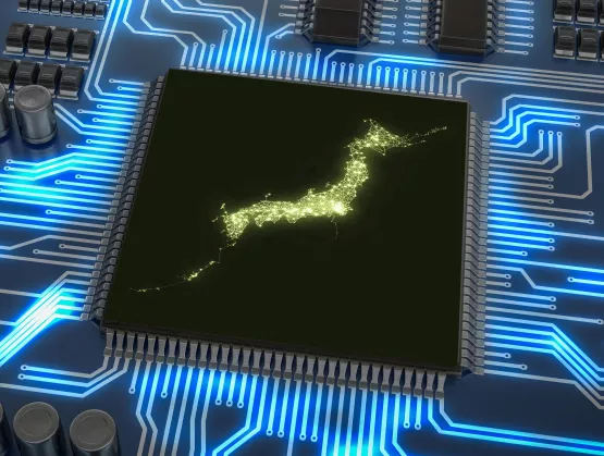
Humanity has survived almost unimaginable challenges over the past 5,000 years of documented human history. From war, famine and natural disasters to the first global pandemic in the last 100 years, more often than not, people have relied on one another to survive and thrive again. As the industry association representing the global microelectronics industry, SEMI has similarly made collaboration and community integral to the fabric of its organization. From helping members to succeed through the COVID-19 pandemic to facilitating member-driven industry standards around environmental health and safety, materials, and manufacturing capabilities, this approach shows members that standing together is better than standing alone.On the eve of the 50th annual SEMICON West (July 20-23, 2020) — the first virtual edition in SEMI’s history — I spoke with SEMI’s vice president of technology communities, Michael Ciesinski, about the role of SEMI in tackling big challenges through an active member community intent on solving problems through collaboration.SEMI: How long have you worked with SEMI and in what capacity?Ciesinski: In January 2016, I started my second tour at SEMI when FlexTech, the industry consortium I’d been leading, became SEMI’s first strategic partner. Nearly two years into that role, SEMI President CEO Ajit Manocha asked me to form Technology Communities to engage members with common interests. After FlexTech, we brought on the Fab Owners Alliance, then MEMS Sensors Industry Group (MSIG), and later the Electronic System Design Alliance (ESD Alliance).SEMI now has more than 20 communities in all, including Smart MedTech, Smart Data AI, Smart Manufacturing, Electronic Materials, and Integrated Packaging, Assembly and Test.SEMI: What is your role with Technology Communities — and how do members stand to benefit?Ciesinski: The leadership of Technology Communities ensures that SEMI’s benefits and services align to our members’ interests so we can provide member benefits that matter most. This spans forming communities where people hold common interests (e.g., advanced packaging) to facilitating standards that will promote intelligence in manufacturing (e.g., data standards for AI and machine learning) as well as providing R D funding.I’m especially proud that over the past three years, SEMI has brought more than $40 million in R D funding to our members, with most grants in the $500,000-$1 million range. We’ve been especially successful in securing funding in flexible hybrid electronics (FHE) through U.S. Army Research Laboratories (ARL), a model we first developed through FlexTech.Two recent recipients of FHE funding, GE Research and ITN Energy Systems, show how the grants are spawning partnership opportunities among commercial enterprises, R D organizations and universities. In developing lightweight, non-invasive wearables, including a human-performance sweat-monitoring patch that remotely analyzes sweat to detect hydration levels and other vital signs, GE Research is using key components such as sensors and lightweight batteries in its designs.ITN Energy Systems designed a flexible all-solid-state lithium battery that’s printed on light, flexible substrates to power small and incredibly thin applications.Universities are also benefiting by plugging into the SEMI ecosystem. In fact, 40-50 percent of funded projects are seeding commercialization by universities. This is another validation that SEMI’s collaborative, community approach to microelectronics is working.SEMI: Position, Timing and Navigation (PNT) is another hot area where SEMI has secured ARL funding. What makes this funding different and why is it important?Ciesinski: The PNT grant makes ARL funding available to the MEMS Sensors Industry Group (MSIG) members through SEMI for the first time. If you’ve ever lost GPS signal while coming out of a tunnel, you know how frustrating that is. For us, that’s an inconvenience, but for a healthcare worker in a remote location who’s waiting for a delivery of medication by drone, it could be life-critical. While that’s just one example of why we need PNT to operate when GPS isn’t available, I can imagine dozens of other important dual-use cases, including autonomous driving.SEMI: How else do Technology Communities benefit under SEMI?Ciesinski: Technology Communities need access to diverse resources to spur continuous innovation. Electronic Materials Group participants, for example, need to stay informed on regulations coming out of Asia, the U.S. and Europe that may affect their businesses. Where else other than SEMI can like-minded stakeholders congregate with people up and down the supply chain to determine whether industry-wide action is needed on regulation?SEMI: What is the importance of SEMI’s global footprint?Ciesinski: I’ve worked with many associations and managed major industry consortia. The clear advantage of SEMI is our global footprint. And that’s vital because microelectronics is a global industry involving a multitude of stakeholders that play essential roles in the supply chain.Let’s say you want to discuss EU regulations on hazardous chemicals. Rather than decipher these complexities alone, you can pick up the phone to speak with someone on SEMI’s European team to learn what’s critical.What if you’d like more information on the 20-plus new fabs that are going up in China? You can explore that question with our SEMI China or SEMI Industry Research and Statistics teams.SEMI: How has SEMI evolved over the years?Ciesinski: SEMI has a long history of providing what the industry cares about. We started in trade shows and pivoted to industry standards. We began with small silicon wafers and wafer carriers, and now within the span of 50 years we’re working on data-format standards that will support the application of AI and machine learning (ML) in the semiconductor industry.While highly varied today, data-format standards will help component manufacturers refine processes to create more efficient solutions. This ARL-funded program, which pairs SEMI members with the grant recipient, Cornell University, may offer dramatic gains in the productivity of semiconductor manufacturing.SEMI: How does SEMI’s approach to COVID-19 reflect core values of collaboration and community?Ciesinski: Together with Ajit Manocha, CMO Terry Tsao and other team members at SEMI, we pulled together a task force to help SEMI members navigate the pandemic.We tapped two existing groups, Environment, Health and Safety (EHS) and Information Technology Leadership (ITL) from the start, documenting their strategic and tactical approaches to help all members through the COVID-19 resource section of our website. The EHS section provides tips on facilities and meetings, employee policies, business travel and communications, while the ITL section lists insights on computing hardware for staff, licensing, networks, security and employee policies.Our EHS leadership team, which includes Entegris, Axcelis, Versum, and Intel, immediately started sharing best practices for sanitizing facilities. As a result of team meetings, SEMI EHS shared best practices on keeping the workforce remote and guidelines for returning people to work safely. From securing PPE and safeguarding employees and visitors by performing thermal scanning to outlining communications around potential employee exposures, EHS has provided meaningful resources for the benefit of all members.SEMI also took immediate steps in the area of advocacy. Our advocacy team in Washington, D.C., together with regional SEMI presidents around the world, have ensured that semiconductor facilities were and still are considered essential businesses in the U.S., Europe and Asia. That’s because microelectronics are foundational to fighting the pandemic.Microfluidics are critical to the Reverse Transcription (RT) Polymerase Chain Reaction (PCR) tests most commonly used for COVID-19. Sensors are embedded in the pulse oximeters that allow patients and healthcare professionals to monitor a vital rubric: oxygen saturation level. If oxygen saturation level drops into the low 90 percentiles or below, it may be time to go to the hospital for treatment.Microcontroller units are essential components in a wide range of hospital equipment, including the ventilators that may make the difference between life and death in the most seriously ill patients.SEMI: How can the ingenuity realized through microelectronics continue to help us tackle other big problems? Ciesinski: We have MEMS and sensors to thank for distributed intelligence, giving us the ability to put sensors anywhere, locally based in the field or in the packaging house.Food production is a prime example. Leveraging miniaturized wirelessly connected sensors, we can trace food through the entire production lifecycle, from the seed in the ground to the food in the warehouse and, ultimately, to the product that lands on the table.From larger enterprise such as IBM Food Trust to small startups, we’re using MEMS and sensors to improve crop yields so we can feed a human population that’s growing each year.There’s a sustainability piece as well. We’re using MEMS and sensors to reduce the amount of fertilizer or other nutrients or chemicals in the soil. That’s good for the environment and for the agricultural workers who labor in the fields.MEMS and sensors can also condense the time it takes to perform a specific task, conserving human resources.SEMI: Where do you think SEMI will go in the next decade?Ciesinski: Ten years from now, I believe we will still have our global footprint in place. I expect it will expand, particularly in Asia.We may also expand into new areas such as Latin America and Central America, which would provide at least two major benefits: People working in microelectronics would, I hope, have access to better quality of life. And diversifying the supply chain would allow nations and regions to have more control over the products they need, from PPE to medications, which may help us to better manage through the next pandemic.I am also hopeful that SEMI will be on the leading edge of helping our members communicate in much different fashion from what we have today. We’re already expanding beyond the paradigm of in-person meetings for standards meetings and conferences. As we move forward, I think we’ll see a hybrid solution to doing business, combining in-person meetings with virtual conferences and digital content that’s available 24/7.Whatever changes we see in SEMI, I’m confident that we will continue to see a global footprint in an industry association that prioritizes connections among members.Engage in the SEMI experience at upcoming SEMICON WestRegister today to hear from keynote speakers such as environmental advocate and former U.S. Vice President Al Gore, futurist and author Steve Brown, and IBM Research senior vice president and director Dr. John E. Kelly III, and Lea Gabrielle, special envoy of the Global Engagement Center for the U.S. State Department, at SEMICON West , July 20-23, 2020. Content will be live streamed and available on-demand. Michael Ciesinski is vice president of Technology Communities for SEMI, the global microelectronics industry association, appointed in August 2018. At SEMI, he directs activity for more than 20 industry groups, oversees the association’s R D funding program, and develops new technology initiatives to serve SEMI’s 2,400 members. Prior to re-joining SEMI, Ciesinski was president/CEO of FlexTech Alliance, an industry consortium focused on new methods of creating electronics. From 1995-2008, Ciesinski served in a similar role at the U.S. Display Consortium (USDC), a private/public partnership chartered with building the infrastructure for electronic display and flexible electronics manufacturing. Both FlexTech and USDC annually sponsor multimillion dollar technology development programs and provide industry technical, financial and market services. Ciesinski is a graduate of the University of Albany, NY, and a former member of the Dean’s Advisory Committee at California Polytechnic State University.Maria Vetrano is a PR consultant at SEMI.
Read More
The COVID-19 pandemic has inflicted major impacts on manufacturing operations worldwide including in the semiconductor industry. The virus has left millions of people confined to their homes, resulting in a massive shift to virtual work and online engagement. In Singapore, where AEM is headquartered, our management team took proactive measures to protect our workers by implementing best practices ahead of the Singapore Circuit Breakers.AEM is globally deemed an essential service, requiring us to maintain operations and minimize impact to our customers. Business continuity plans that include work-from-home and safe-distancing guidelines are in place. As of the time of this writing, we are very fortunate that all of our employees are safe and that we’ve seen only minimal impacts to our customer commitments. AEM has confined this impact by spreading operational risks across our facilities in Asia, Europe, the U.S. and divisions in Singapore, Malaysia, China, North America, Central America, Finland, France and Vietnam. All told, these facilities employ more than 550 people (Figure 1).Figure 1 – AEM Global Presence As a global leader, AEM offers application-specific intelligent system-level test and handling solutions for semiconductor and electronics companies that serve the advanced computing, 5G communications and artificial intelligence (AI) markets.Leveraging our decade of experience, the latest AMPS solutions provide asynchronous, modular, massively parallel and smart system-level testing to meet the new test challenges of complex ICs. The modularity and scalability of these systems enables customers to scale their existing engineering device validation solutions into high-volume, massively parallel production solutions that increase faults coverage, reduces time to market, and decreases cost of test and ownership (Figure 2).Figure 2 – AMPS System-Level Test Solution In meeting 5G infrastructure test needs, AEM developed a field-deployable fiber optics tester. Called WideOptix SR4, the system was initially developed in collaboration with a world leader to support the 5G fiber infrastructure deployment in China and has now been adopted for some Ethernet standards testing. With our WideOptix SR4 development, we cultivated Silicon Photonics (SiPh) testing expertise that complements our AMPS system-level test capability. As part of our business continuation and risk diversifications plan, we had also set up factories in Penang (5,200m2) and Suzhou (3,600m2). Penang’s rising influence in the Southeast Asia semiconductor industry has prompted AMM (AEM Malaysia) to expand its scope to include value-added services with a Center of SSD Excellence and Center of Photonic Excellence.ASZ (AEM Suzhou) will continue to focus on the domestic market in China for further expansion and penetration with products ranging from cost-sensitive testers to state-of-the-art test measurement instruments. In Europe, AEM is focused on wafer-level test and cost-effective ATE test solutions. Finland-based AFORE specializes in MEMS and application-specific wafer testing with the ability to add physical stimulus. The company's state-of-the-art instruments enable the testing of devices such as diced IMU’s (Inertia and Motion Units) in continuous rotation on a wafer mounting ring. Our process increased test throughput by 3X compared to the traditional pick-and-place methods (Figure 3).Figure 3 – Wafer-Level Test Throughput Advantage A specialist in application-specific wafer handling, AFORE developed its latest design to support quantum computing in collaboration with its partner BLUE FORS. The company’s probing equipment features a handling solution with temperature tolerances to 2K (-270’C) to support cryogenic testing (Figure 4).Figure 4 – Cryogenic Quantum Computing Probing Solution AFORE also gained critical insights into creating total darkness, enabling us to further explore opportunities for dark matter testing. AFORE is currently in talks with a member of the LUX Photonics Consortium funded by the National Research Foundation (Singapore) to provide a dark body testing environment and handling for its IR detectors.In Europe, our acquisition of Mu-TEST in France helps diversify our product and service offerings while spreading our business continuity risks. Mu-TEST enjoys collective test-development experience of more than 320 man-years thanks to various ATE suppliers including Schlumberger and Credence. To help combat rising costs of traditional ATE, Mu-TEST developed cost-effective solutions using FPGA-based instruments supported by a full suite of test development, debug and production test software with links to EDA and standard interfaces. This provides Mu-TEST an agile platform that can be easily re-configured for different customer needs.This Mu-Test acquisition expands AEM’s system-level testing capability to include Functional Test, allowing BIST, SCAN, JTAG to test structural failures and perform other application-level test that interface directly with the DUT using the EVM (Electronics Validation) boards to increase fault coverage within the same test environment. Mu-TEST has also enabled AEM to form the recent partnership with UTAC to develop a cost-effective CIS test solution that addresses UTAC’s test needs and complements its CIS advanced packaging solutions. Our U.S. headquarters based in Chandler, Arizona has expanded its capabilities to provide application engineering.In summary, AEM has been expanding its global footprint while managing risk and has been fortunate to be positioned to manage the recent COVID-19 excursions. While each geographical location specializes in core technologies, all sites have access to one another’s manufacturing facilities in times of need and a pool of IP available to address new opportunities. We believe this risk diversification positions us well to serve the needs and interests of our customers worldwide.Lo Wee Tick is Director, Business Development, and Stuart Pearce is Senior Director, Field Marketing, at AEM Holdings Ltd.
Read More
Emerging applications powered by 5G and artificial intelligence (AI) are expected to be a boon to the semiconductor industry, but only once chipmakers overcome a key challenge: Architecting chips that meet the exacting performance, power consumption, size and cost requirements of devices for mid- to high-end applications. One technology – heterogeneous integration – promises to meet these demands and help drive future leaps in semiconductor innovation in the post-Moore era. To help the industry better grasp the technology challenges and business opportunities associated with deploying highly integrated chip and packaging technologies, SEMI and AI on Chip Taiwan Alliance recently gathered industry leaders from organizations including ASE, Unimicron, Dialog Semiconductor, Cadence and AITA to discuss technology trends and the vital importance of building a cross-industry exchange platform to advance next-generation manufacturing processes critical to heterogeneous integration. Following are key takeaways from the forum, Heterogeneous Integration Enables 5G and AI. Overcoming Heterogeneous Integration Technology Challenges Key to Advances in Taiwan High-End Semiconductor Manufacturing The introduction of the Heterogeneous Integration Roadmap (HIR) by the International Technology Roadmap for Semiconductors team in 2016 was an important first step, Dr. C.P. Hung, Vice President of ASE Group, noted in his opening remarks. The HIR is designed to stimulate pre-competitive collaboration to advance heterogeneous integration technology development and accelerate electronics innovation. The roadmap provides a long-term vision for the electronics industry, identifying future technology requirements and potential solutions. Today, the HIR working group focuses on high-performance computing (HPC), 5G and other leading-edge technologies.Dr. Hung predicted that heterogenous integration will reshape traditional collaborations between the semiconductor ecosystem and supply chain in order to clear I/O bottlenecks that hamstring high-performance applications. The retooled industry connections will also need to enable high I/O pin counts, ultra-thin devices, and high-frequency signal shields. In an important step forward, the chip industry today is developing a platform that enhances wafer-level advanced packaging services and deepens cooperation with Oversea Assembly and Testing (OSAT) and substrate supply chain partners. Overcoming the current limits of IC substrates – the connection between IC chips the PCB – is one key for heterogeneous integration technology to flourish, said Dr. Yu-Hua Chen, Vice President, Carrier SBU, RD Division of Unimicron. He noted that the industry must tackle limits to PCB thickness, substrate density, fine pitch and automation to meet the needs of high-end packaging customers. Another barrier the industry must be surmounted is to make the currently inscrutable confidentiality requirements for patents of foreign materials – key to improving chip yields – easier to access and understand for substrate engineers. Chen said partnerships across the entire industry will be necessary to break through this and other technology breakthroughs. Supply Chain and Cross-Border Ecosystem to Strengthen Partnerships for Further DevelopmentTaiwan has long invested heavily in advancing semiconductor manufacturing and application engineering technologies to become a top global chipmaking hub and, in the process, has been behind significant leaps in optimizing chip functionality, said Leroy Liu, General Manager, Asia Headquarters, of Dialog Semiconductor (Germany). With its semiconductor manufacturing prowess, Taiwan can also play a central role in maturing advanced heterogeneous integration packaging technology while managing development costs by partnering with its international supply chain community to overcome technical challenges more effectively, Liu said. The region can also help forge partnerships, even among competitors, to build the ecosystem essential for heterogeneous integration technology to shine.EDA tools will be critical in understanding and resolving heterogeneous integration technical issues since IC substrate, packaging and chip design all pose interdisciplinary engineering challenges, said Julian Sun, Product Marketing Director at Cadence. To help the industry navigate these challenges, Cadence has launched intelligent system design products – solutions that address a wide range of design problems with semiconductor nanometers, micrometers on packaging and testing, and PCB level micro/millimeters to Pin/Pitch, I/O models, and thermals and electricity. By supporting various technical designs, Cadence helps customers shorten the design cycle to strengthen design quality and reduce costs.Sun also pointed to the vital importance of overcoming the significant challenge of designing silicon interposers for heterogeneous integration. Today’s EDA tools are capable of optimizing the design of complex structures including 5GAiP and HBM and are instrumental in aiding Taiwan’s semiconductor ecosystem players to quickly adapt to shifts in the evolving heterogeneous integration market.Heterogeneous Integration Enables 5G and AI speakers (L-R): Julian Sun, Product Marketing Director at Cadence, Dr. Yu-Hua Chen, Vice President, Carrier SBU, RD Division of Unimicron, Dr. C.P. Hung, Vice President of ASE Group, Leroy Liu, General Manager, Asia Headquarters, of Dialog Semiconductor (Germany), Dr. Shih-Chieh Chang, AITA Executive Secretary Designing AI chips is particularly difficult as semiconductor makers struggle with high costs and low yields, said Dr. Shih-Chieh Chang, AITA’s Executive Secretary. That’s why the chip industry now uses FPGAs for small-volume production of AI chips, which makes it easier to improve manufacturing yield through redundant design. For its part, AITA has formed a special interest group (SIG) to help form connections among the chip industry, academia and research institutes. The association’s goal is to build a platform for mass production of AI chips.To get involved in SEMI Taiwan Heterogeneous Integration related events, please contact Ula Huang, outreach senior specialist, at [email protected] Fang is a coordinator and Ashley Huang is a specialist in marketing and public relations at SEMI Taiwan.
Read More
The world’s most advanced manufacturing factories are leading the way in driving efficiency and sustainability.In advance of its 2020 meeting, the World Economic Forum welcomed Micron into its Global Lighthouse Network, a group of advanced manufacturers “that are showing leadership in applying the technologies of the Fourth Industrial Revolution to drive operational and environmental impact.”For years, Micron has been helping clients integrate artificial intelligence (AI), big data analytics and the industrial internet of things (IIoT) into their factories. And now Micron’s factory is one of the first facilities in Singapore, along with Infineon, to be recognized by the Global Lighthouse Network.In a recent interview with Channel News Asia, Manish Bhatia, executive VP of Global Operations, explained how Micron has been practicing what it preaches: “Our products enable new technology trends such as IoT, 5G, cloud computing and autonomous driving. Applying these technologies in our own manufacturing facilities demonstrates the enormous potential in driving business value. Industrial IoT and artificial intelligence are part of the biggest revolution since the advent of robotic manufacturing productivity 50 years ago.”For Micron, this journey started with the need to “keep pace with the technological advancement of our semiconductor processes,” Manish said. “We wanted to provide higher-capacity, higher-performance, lower-cost and lower-power chips.”This meant embarking on the same journey they guide clients through: “We started by focusing in 2014 on simple statistical analysis to improve our production processes,” Manish said. “Following that, we developed more complex deep learning and AI capabilities to draw insights from our data. Most recently, we introduced IoT sensors — like cameras and acoustic sensors — to gather even more data that allows us to further improve our production processes.”The Singapore factory plays a critical role in developing leading-edge NAND. Micron’s Singapore presence, composed of two wafer-fabrication facilities and one assembly and test facility, serves as the base for worldwide operations. With over 500,000 square feet of cleanroom space, the location is also a designated NAND Center of Excellence, driving the implementation of the company’s leading-edge 3D NAND production for use in mobile phones, solid-state drives, digital cameras and more. Micron employs approximately 8,000 people in Singapore.The World Economic Forum says the results of the Singapore transformation have been spectacular: Micron’s “semiconductor fabrication facility has integrated big data infrastructure and IIoT to implement artificial intelligence and data science solutions, raising product quality standards and doubling the speed at which new products are ramped.”Below are notable achievements that Micron was recognized for: Automation of production and maintenance produced a 4% tool availability improvement. The IIoT-enabled smart factory led to a 22% scrap and product downgrade reduction. Advanced analytics for process optimization with OEMs reduced time to ramp new products by 50%. Deep learning optical-defect detection created a 2% yield improvement. The integrated deviation management platform reduced time to resolve quality issues by 50%. Micron was a natural choice for the Global Lighthouse Network, an organization whose creation is timely. The World Economic Forum points out that “global production industry is lagging in its adoption of Fourth Industrial Revolution manufacturing technologies, with more than 70% of companies stuck in pilot-phases … [There is] a need for a neutral learning platform to showcase top-use cases, roadmaps and organizational approaches to adopting and scaling technologies from which other companies globally could benefit.”As part of the Global Lighthouse Network, Micron will be able to share knowledge and best practices with peers, support new partnerships and help other manufacturers deploy technology, adopt sustainable practices and transform their workforces. We can all build on this community of like-minded organizations, levering technology to improve efficiencies and promote sustainability.This recognition from the World Economic Forum is a win-win. We look forward to joining the club of lighthouse factories around the world and to helping propel the entire global manufacturing industry into the Fourth Industrial Revolution. At Micron, we are at the forefront of this transformation and welcome the opportunity to serve as a lighthouse.Koen De Backer is responsible for driving Micron’s smart manufacturing initiatives and digital operations including capabilities with IoT, artificial intelligence, advanced analytics, cognitive computing and machine learning to enhance Micron’s business, global operations and product development. Prior to joining Micron, Mr. De Backer led large-scale operations projects for more than a decade to help clients reduce inefficiencies and achieve excellence in manufacturing, procurement, supply chain and support functions.Most recently, De Backer was a partner at McKinsey Company, where he steered the semiconductor consulting practice in Southeast Asia and was one of the firm’s leading experts on applying artificial intelligence and automation techniques across operations and support functions such as finance, human resources and procurement. Additionally, Mr. De Backer consulted with high-tech global clients while working at Deloitte Consulting, Altran Europe and CSC. Mr. De Backer holds a master’s degree in business administration from INSEAD and a master’s degrees in both industrial management and electromechanical engineering from Katholieke Universiteit Leuven.De Backer is also chairman of the SEMI Southeast Asia Smart Manufacturing Chapter. For information on participating in the chapter, contact Shannen Koh at [email protected].
Read More