downloadGroupGroupnoun_press release_995423_000000 copyGroupnoun_Feed_96767_000000Group 19noun_pictures_1817522_000000Member company iconResource item iconStore item iconGroup 19Group 19noun_Photo_2085192_000000 Copynoun_presentation_2096081_000000Group 19Group Copy 7noun_webinar_692730_000000Path
Skip to main content
Default Banner Image

Artificial Intelligence

New SEMI Taiwan Testing Committee to strengthen the last line of defense to ensure the reliability of advanced semiconductor applications.Mobile, high-performance computing (HPC), automotive, and IoT – the four future growth drivers of semiconductor industry, plus the additional boost from artificial intelligence (AI) and 5G – will spur exponential demand for multi-function and high-performance chips. Today, a 3D IC semiconductor structure is beginning to integrate multiple chips to extend functionality and performance, making heterogeneous integration an irreversible trend. As the number of chips integrated in a single package increases, the structural complexity also rises. Not only will this make identifying chip defects harder, but the compatibility and interconnection between components will also introduce uncertainties that can undermine the reliability of the final ICs. Add to these challenges the need for tight cost control and a faster time to market, and it’s clear that semiconductor testing requires disruptive, innovative change. Traditional final-product testing focusing on finished components is now giving way to wafer- and system-level testing.In addition, the traditional notion of design for testing, an approach that enhances testing controllability and observability, is now coupled with the imperative to test for design, which emphasizes drawing analytics insights from collected test data to help reduce design errors and shorten development cycles. Going forward, the relationship among design, manufacturing, packaging, and testing will no longer be un-directional. Instead, it will be a cycle of continuous improvement.This paradigm shift in semiconductor testing, however, will also create a need for new industry standards and regulations, elevate visibility and security levels for shared data, require the optimization of testing time and costs, and lead to a shortage of testing professionals. Solving all these issues will require a joint effort by the industry and academia. "With leading technologies and $4.7 billion in market value, Taiwan still holds the top spot in global semiconductor testing market," said Terry Tsao, President of SEMI Taiwan. "When testing extends beyond the manufacturing process, it can play a critical role in ensuring quality throughout the entire life cycle from design and manufacturing to system integration while maintaining effective controls on development costs and schedules. Taiwan's semiconductor industry is in dire need of a common testing platform to enable the cross-disciplinary collaboration necessary for technical breakthroughs."The SEMI Taiwan Testing Committee was formed to meet that need, gathering testing experts and academics from MediaTek, Intel, NXP Semiconductors, TSMC, UMC, ASE Technology, SPIL, KYEC, Teradyne, Advantest, FormFactor, MJC, Synopsys, Cadence, Mentor, and National Tsing Hua University to collaborate in building a complete testing ecosystem. The committee addresses common technical challenges faced by the industry and cultivates next-generation testing professionals to enable Taiwan to maintain its global leadership in semiconductor testing.The SEMI Taiwan Testing Platform spans communities, expositions, programs, events, networking, business matching, advocacy, and market and technology insights. For more information about the SEMI Taiwan Testing platform, please contact Elaine Lee ([email protected]) or Ana Li ([email protected]). Emmy Yi is a marketing specialist at SEMI Taiwan.
Read More
We are living in a digital world where semiconductors are taken for granted, AI is bringing semiconductors back into the deserved spotlight, and now we are witnessing the dawn of the Cognitive Era enabled by semiconductors,” SEMI president and CEO Ajit Manocha said to an audience of more than 500 during his presentation – Rebirth of the Semiconductor Industry – at the First Global IC Entrepreneur Conference.Speaking at the Shanghai event in mid-December, Manocha recalled how, when he first entered the semiconductor industry in the 1980s, semiconductors revenue topped out at about $10 billion. Now, with sales having swelled to a staggering $450 billion, the industry is on a much faster growth track. Revenue could reach $500 billion by the end of 2020 and trillions of dollars by 2030. Over the past two decades, chips have given rise to social media and e-commerce powerhouses such as Google, Facebook, and Alibaba. All rely on heavily on chips, the engines of data centers across all industries. Wave after wave of technology innovation have been powered by semiconductors – from mainframe computers in the 1970s, personal computers in the 1980s, the Internet in the 1990s, and mobile and social networking in the early 20th century, to the current shining stars of technology such as IoT, big data, new memory, virtual reality, autonomous driving and artificial intelligence, Manocha said. New applications across areas such as smart manufacturing and digital healthcare are stoking the latest round of semiconductor growth.The rise of AI, like all the technologies before it, has renewed the semiconductor industry once again with its promise to drive growth of all industries worldwide, Manocha said. Five years ago, IoT was but a gleam in a technologist’s eye, more hype than reality with doubt about its viability running deep. Today, with about 60 percent of people in the world connected to the Internet, the enormous promise and potential of IoT is flowering. Industry growth will explode as the melding of AI and IoT birth countless applications and innovations in SMART transportation (0 emissions; 0 fatalities; 0 congestion), smart sensors (agriculture, infrastructure, healthcare) and SMART “Everything” (people, devices, homes, cities, industries, and the list goes on). Indeed, AI is now widely recognized as a chief growth driver of the semiconductor industry well into the future, with semiconductor technology at the core of AI innovation, he said. Semiconductors are thrusting the fifth industrial revolution into the fast lane. China’s much-anticipated rise as an industry powerhouse over the next few years will only accelerate industry growth, turning current disruptions into future opportunities as SEMI China continues to cultivate connection, collaboration and innovation in China’s fast-growing semiconductor sector.Cherry Sun is a marketing manager at SEMI China.
Read More
4 Key Takeaways from SEMI Taiwan Member ForumThe rapid development of artificial intelligence (AI) has accelerated the digital transformation in various industries and has now fused with Internet of Things (IoT) to exploit the value of both technologies in reshaping the electronics industry value chain. As it emerges from the shadows of its parent technologies, AIoT is giving rise to new opportunities in manufacturing, healthcare, transportation, and even energy. AIoT is fast rising in prominence as an enabler of key electronics manufacturing process improvements and the creation of add-on value to existing products – both critical to the success of many businesses.SEMI and the SEMI MEMS Sensors Industry Group (SEMI-MSIG) held a technical forum on smart sensing and its applications in AI and AIoT, inviting renowned experts in sensors and edge computing to share in-depth insights into the latest AIoT technologies and applications with more than 100 industry professionals in research and development, marketing and sales. Here are four key takeaways from the SEMI Taiwan member forum.1. Steady Growth for Global Sensors MarketThe global sensors market’s steady growth is expected to expand at a CAGR of 6.6 percent from 2017 to 2023, with Asia driving the biggest gains and automotive leading the segments – including healthcare and education – with the strongest growth. Automotive alone is expected to reach US$34 billion in 2023.2. Integration Critical to MEMS Sensors DesignsWith AI booming, MEMS sensor designs need to drive toward greater integration —not only integrating data collection with sensors, but also streamlining data processing on the backend – making 3D models of today’s MEMS mechanical designs critical. The differences between 3D and entrenched 2D models are dramatic, elevating the importance of specifying manufacturing steps in MEMS designs. As new sensors and applications continue to emerge, companies that develop the most powerful integrated designs will win. 3. Growth of Smart Voice-Control Applications to ExplodeAIoT is also accelerating the development of smart voice-control applications and the rise of new related business opportunities. Just 50 million voice-controlled devices shipped worldwide in 2017, a number predicted to swell to 436 million in 2021 with smart home devices such as set-top boxes and smart TVs the major growth drivers.4. AIoT Eyed to Make Human-Robot Collaboration SafeSafety is an essential feature for human-robot collaboration. Tactile sensing technologies give robots a layer of “skin” with capabilities rivaling human touch. To ensure humans and robots work together safely in work environments, sensors on this layer of skin are concentrated – less than 8mm apart, equivalent to the width of a human finger, with a response time of less than 5ms on contact. More than 4 million robots worldwide are expected to be upgraded with these sensing technologies and are on track for deployment in pilot plants in the next three years.SEMI-MSIG is committed to strengthening connections across all sectors in the MEMS and sensors supply chain, working closely with the industry to accelerate the development of related technologies and applications in both mature and emerging markets. In addition, SEMI-MSIG hosts regular events to inspire business opportunities and technology exchange for innovative applications, while enhancing the visibility of members among global customers and partners to help them forge new partnerships. To join the group, contact SEMI Taiwan’s Helen Chen at [email protected] Yi is a marketing specialist at SEMI Taiwan.
Read More
Semiconductor fabs have been getting smarter and smarter over the past 30 years. It’s a natural evolution – the direct outcome of numerous continuous-improvement efforts. The really important difference on the road to smarter fabs, the one change that’s enabling the Industry 4.0 revolution, is the concept of a cyber-physical system or digital twin. If you don’t have a thorough, detailed, high-fidelity digital twin of your entire fab operation, then you cannot have “Smart Manufacturing.” That’s really the definition of a smart site. A digital twin is simply a requirement for all smart factories of the future. One caveat: No matter what you build today from a smart perspective, your digital twin’s fidelity will improve over the next 20 years. A factory’s digital twin has two facets: the operational aspect and the yield aspect. Each of these two facets places different requirements on a database including the types of data, the frequency of data generated, the retention of data, and even the AI/ML techniques used to analyze the data. A combination of these data requirements are needed to create a digital twin – the virtual representation of your entire factory operation, whether it’s on the wafer-fab front end or the assembly and test back end. What’s most important here is that facility-wide data sets and databases must be able to communicate with each other using refined summary statistics to create a practical digital twin. For example, a lot of information is collected on the yield side to feed the deep-learning models needed to manage processes. However, the factory scheduler, driven largely by the smart operational database, needs only summary statistics from the yield database to be able to act in the next moment or over the next 24 hours. Figure 1 illustrates the needs of and the interaction between a smart operational and a yield database. Figure 1: The Operational and Yield databases in a Smart Factory need to exchange summary statistics. Today, we find that although these databases generally speak to each other in smart factories, they’re still not sufficiently connected to permit the use and analysis of data needed to realize the full potential of a smart factory. That level of interconnectedness is still in the future. Some solution providers have created what is essentially a “smart learning warehouse” (“database” has become too limited a term here). This warehouse collects, analyzes and learns from the extensive amount of information that a fab generates. Game-changing, more holistic applications become possible when this information can be combined in new and informative ways. As it turns out, a data source is just a data source, but users in different factory areas need to extract different information from these common data sources. They need different applications and portals – in other words “views” – that are adapted and adjusted for each area’s needs. Aren’t we smart enough? Some people think that 300mm fabs are already smart. That’s true. They are. But, they could be a lot smarter. No 300mm fab in use today has attained the full, utopian vision of what a smart factory can deliver over the next 10 years. When you finally integrate all of the disparate databases in a fab – when you’re able to use all of those different data sources as one common data source – that’s when your Smart Factory will have the ability to self-optimize its future actions and react quickly to real-time events. The largest semiconductor manufacturers tend to develop these smart factory applications on their own. The remaining semiconductor fabs need to work together with other fabs and their solution providers to develop these smart factory applications. Why now? Why is everyone talking about “Smart” now? It’s because the semiconductor industry has helped to create all of the enabling technology: the compute power, the networking and networking standards, and even the industry’s maturation into a multi-tiered organization of solution providers. We’ve reached the point where we can collect data from a widespread sensor network along with tool-health data and we can then warehouse this data so that it can be applied to more intelligent decision-making. While there may be one or two sensors on a tool today, in the future there will be many such sensors connected over an IoT network or networks that provide mountains of data to the warehouse. All of this data will feed into the digital-twin version of the fab. One of the biggest changes on the horizon made possible by all of this accessible data is advanced scheduling. Despite all of the automation advancements made over the past 25 years, including robotic handling, it’s still hard to decide “where, what, and when?” for every single lot in the factory. Today, no factory in the world is more complex than a semiconductor fab. Optimizing a semiconductor manufacturing process is the most complex manufacturing-optimization task in the world. Do it for ROI ROI is the chief reason for having a digital twin. Once you can make a truly smart, holistic schedule of the fabs operations — not a dispatch or rule-based dispatch list — then you can create an operationally smart factory. Rule-based dispatching systems primarily focus on tools and tool-centric views. Although they incorporate knowledge from current WIP and tool conditions to make decisions better than simple dispatch systems, smart factories are not just about tools and the current WIP at them. Smart factories use the status of every tool and lot in the factory to make fab-centric optimizations instead of tool-specific optimizations. Once you have a digital twin, you’re optimizing for global functions such as line linearity and on-time delivery. These functions are not just about the moment. The transition to a smart factory thus represents a huge philosophical change. When you know exactly what’s going to happen in a factory over the next 12 hours for every single lot, every single wafer carrier, and every single entrance port of every tool in the factory, then you suddenly have control over the factory’s idle time. You know when you can optimally perform PM (preventive maintenance). You know how to best redirect material or labor resources to maximize output. You can create a smart schedule for every maintenance person in the factory that comprehends each person’s skill set and tool downtime so that there’s no negative impact on the factory’s productivity. You can only do all of this when you know the future. Figure 2 illustrates the opportunity. Imagine that a factory contains 1,500 tools. Use of these tools is scheduled for the next twelve hours. The information depicted in Figure 2 encompasses process changes from one chemistry to another, implant changes, reticle changes, and the status of every single consumable for all 1,500 tools. The white spaces that appear between processes in Figure 2 represent opportunities to intelligently schedule events such as maintenance to maximize factory productivity. Figure 2: Smart scheduling permits factory-wide optimization to maximize productivity. Once you have a schedule, you need to translate that schedule into actions or movement. It’s not easy to do this and most material-control systems today make overly simplistic decisions based on modeled assumptions and typical cases rather than the actual time each lot needs to be at a precise location, which can only come from a schedule. Once the data from all of the tools is connected, a smart scheduling system can use the digital twin to make far better process decisions. The larger the factory (or more complex the factory), the more important it is to make smarter decisions. Note: SEMI has a Smart Manufacturing Technology Community. For more information or to get involved, click here. If you would like to discuss Smart Manufacturing more with John directly, he can be contacted at [email protected]. John Behnke is general manager of the Final Phase Systems product line at INFICON.
Read More
Artificial intelligence (AI) is on the verge of transforming entire industries as it gears up to power semiconductor industry innovation and growth, thrusting the technology to front and center at SEMICON Japan 2019, December 12-14 at the Tokyo Big Sight (Tokyo International Exhibition Center).The SMART Technology Forum at SEMICON Japan will highlight the latest AI developments and trends. Supported by U.S. Commercial Service in Japan, the forum will feature Yutaka Matsuo of the University of Tokyo. An authority on AI, Matuso will give an overview of both AI business and technology. His presentation will be followed by an AI outlook from Microsoft Japan, Amazon Web Services and DefinedCrowd.A number of Japanese startups are on leading edge of AI innovation in machine and deep learning. One is Preferred Networks Inc., a company that applies cutting-edge deep learning technology to Internet of Things (IoT) applications across transportation, manufacturing and healthcare.In his opening day keynote at SEMICON Japan, Toru Nishikawa, president and CEO of Preferred Networks, Inc., will highlight the latest developments and promise of using deep learning for industrial applications. Nishikawa will unpack how AI companies jockeying for competitive advantage will win by harnessing technologies to process massive amounts of data efficiently and quickly.Following is look at Preferred Networks, Inc. and five other Japanese startups that are driving AI innovation. Within Japan's world of AI, machine learning, and deep dearning, Preferred Networks is likely the most well-known Japanese company. The parent company, Preferred Infrastructure, was founded in March 2006 by Toru Nishikawa and Daisuke Okanohara, who focused on search engine development before turning to machine learning and establishing Preferred Networks to commercialize the technology.Preferred Networks established itself as one of the world’s top providers of machine learning technology with the development of Chainer – an open source deep learning framework that has been offered free of charge since June 2015 and was released before TensorFlow, Google’s renowned Deep Learning framework. Established in 2012, ABEJA is thought to be Japan’s first venture company to specialize in deep learning. ABEJA's core technology is its AI platform ABEJA Platform. Based on this platform, the company offers various solutions to more than 100 client companies. ABEJA also offers ABEJA Insight, a specialized package service for the retail and distribution, manufacturing, and infrastructure industries. Data analytics provider BrainPad Inc. was the first Japanese AI venture listed on the Tokyo Stock Exchange. Established in 2004, before the advent of big data, BrainPad Inc. cultivated a vision of analyzing vast amounts of data in increase the competitiveness of Japanese companies. LeapMind Inc. aims to offer deep learning technology that uses fewer computing resources and draws less power. Both are important capabilities since deep learning requires considerable computing resources to perform image and speech recognition. The company’s answer to this deep learning challenge is a small form factor FPGA with low power consumption.In April 2018, LeapMind started offering the tool DeLTA-Lite to support model construction for Deep Learning. The tool simplifies the development of deep learning design models, eliminating the need for model design, hardware, and software expertise. Hacarus Inc.’s HACARUS-X AI technology, which combines sparse modeling and machine learning technology, features low power consumption and small devices such as FPGAs. In collaboration with semiconductor trading company PALTEK, Hacarus is integrating HACARUS-X algorithms with Xilinx's FPGA Zynq UltraScale + MPSoC. Both companies area also implementing HACARUS-X algorithms in a box computer.Sparse modeling is gaining attention as a modeling method by which humans can understand the judgment process of AI by extracting features from a small amount of learning data. With expertise in life science fields such as medical and biology and image processing technology, LPixel, Inc. develops image analysis systems with original algorithms and machine learning techniques. It has developed a cloud-based AI image analysis platform and an AI medical image diagnosis support technology that streamlines the review of large amounts of research data and detects image fraud in research papers and other documents for the medical and biology fields, freeing researchers to devote more time to their core work. Yoichiro Ando is a marketing director at SEMI Japan.
Read More
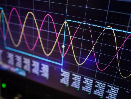
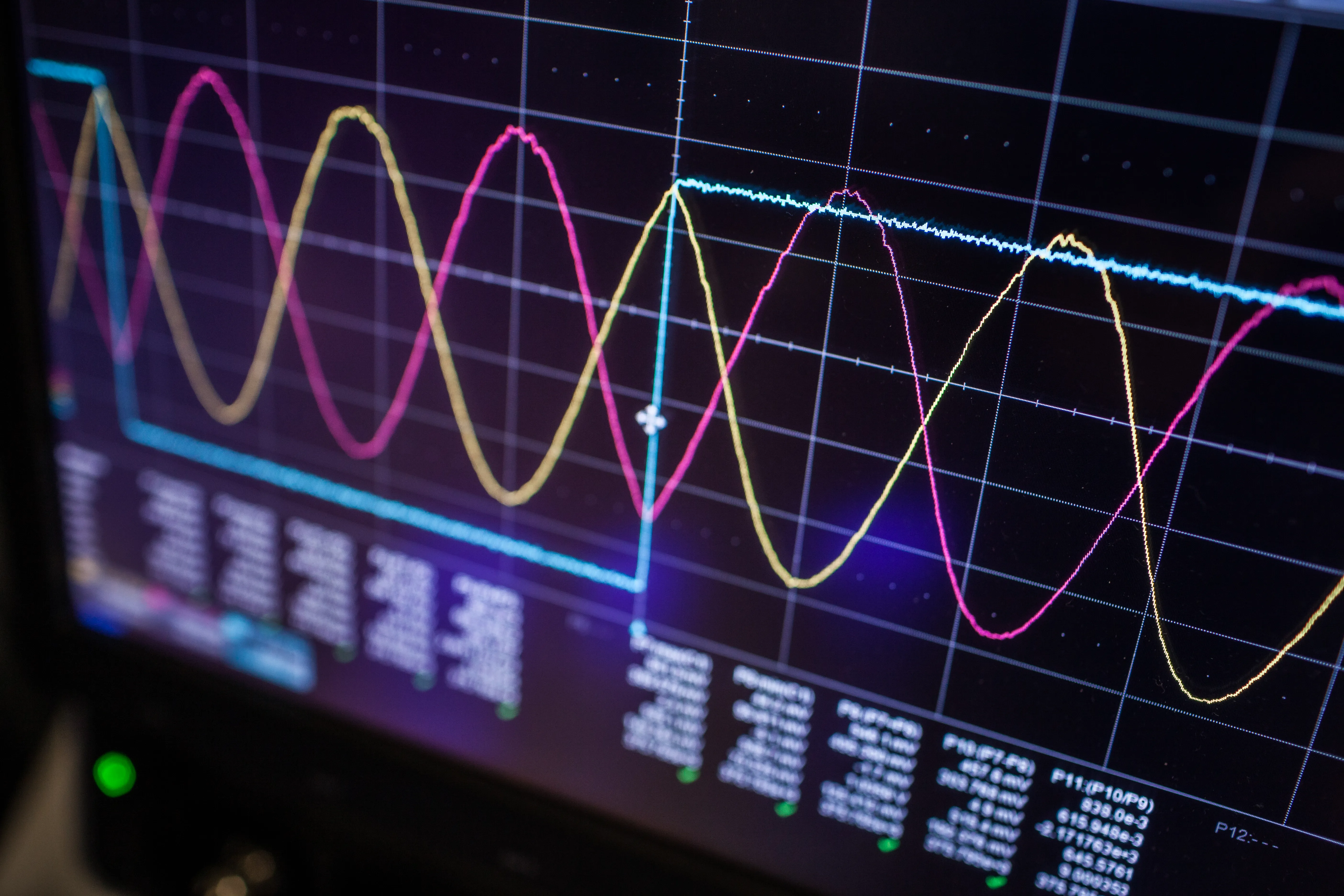
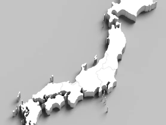
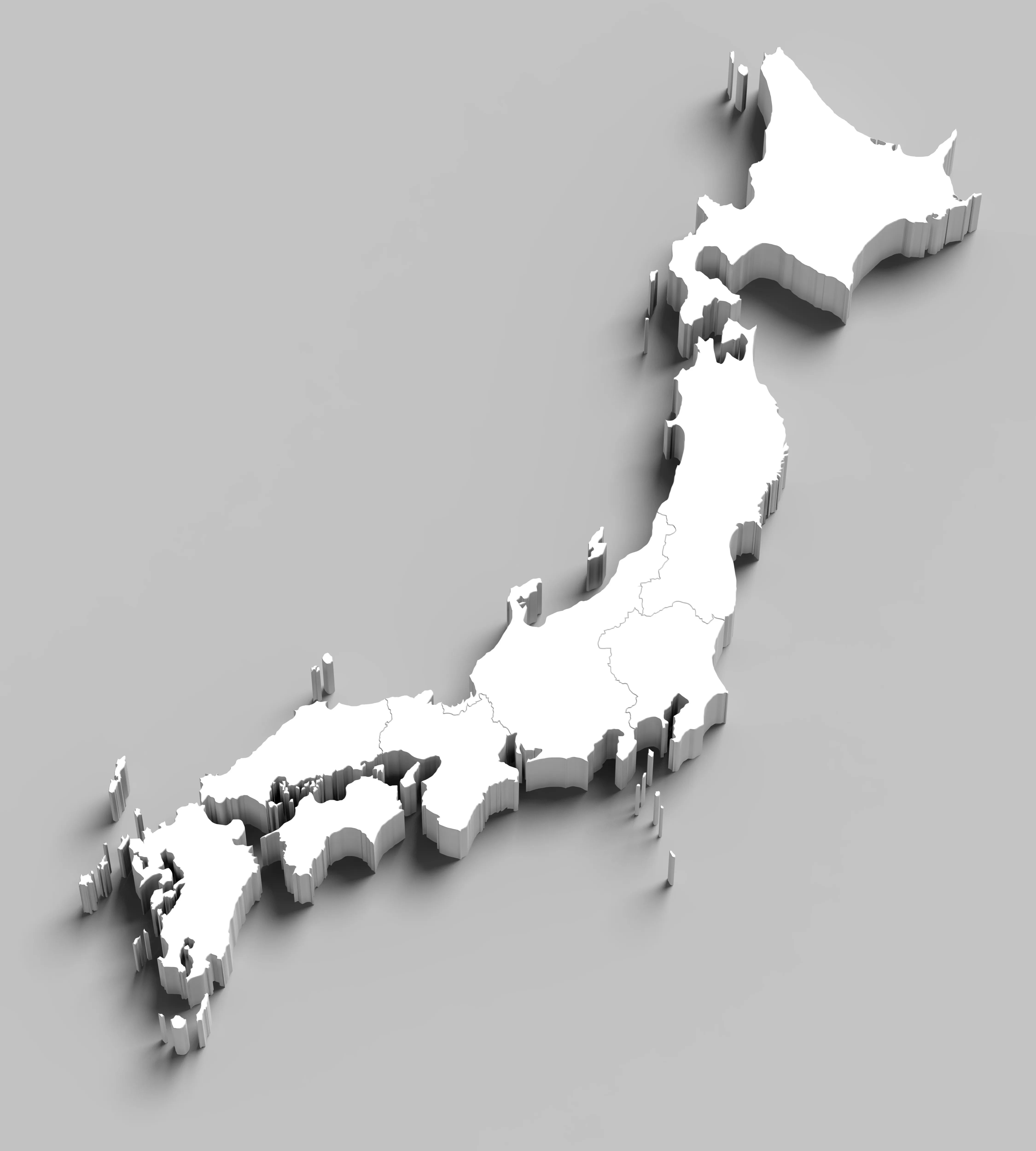
Kyushu, the third largest island in Japan, is home to the semiconductor production bases of integrated device manufacturers (IDMs) with world-class cutting-edge technology. SONY, Toshiba, Hitachi, Mitsubishi, Fujitsu and Nissan are among the sector’s shining stars, though a host of other IDMs tied to the supply chains of other major enterprises have also set root in Kyushu. Collectively, the companies earned Kyushu the name Silicon Island of Japan.Kyushu’s flourishing IDM industry sprouted from favorable tax and other government policies that reduced semiconductor production costs to levels lower than elsewhere in Japan. Once the IC producers had established bases, equipment and materials companies naturally followed, leading to the influx of many parts manufacturers. Together, they came to Kyushu, one after another, to make the island a magnet for manufacturing. And so it was to Kyushu that a SEMI China delegation travelled for a meeting at TEL’s factory in Kumamoto to learn more about the secrets to the rapid growth of the island’s semiconductor industry and promote cooperation between Chinese and Japanese enterprises. Underscoring the rise of the Silicon Island of Japan, China will soon become TEL’s largest market, said Masami Akimoto, Chairman of Tokyo Electron Kyushu Limited, speaking at the event. Masami Akimoto hopes for support from SEMI China.The island of 12 million people contributes to the growth of the global semiconductor industry, expected to reach USD 500 billion in size in 2019 as China’s semiconductor sector, fueled in part by government-backed investment funds, continues its rapid expansion. Despite the gains, China still lags other regions in advanced manufacturing, said Lung Chu, president of SEMI China, which is doing its part to draw more advanced manufacturing to the region through its SIIP platform. The initiative encourages pan-regional cooperation with China’s semiconductor industry to promote free trade, open markets, technology innovation and IP protection – all to help China better integrate with the global semiconductor industry. SEMI China President Lung Chu(L) issues visit memorial to Masami Akimoto(R), Chairman of Tokyo Electron Kyushu Limited. Chicken shall be led by the HenUnlike other regions with comprehensive semiconductor industries, Kyushu’s is primarily focused on production and assembly, with more than 200 manufacturers of semiconductor equipment and parts.SEMI China Delegation at Tokyo Electron Kyushu LimitedTEL built its first factory in Kumamoto, a city covered by volcanic ash in the center of Kyushu, 34 years ago. Today, TEL every month produces 80 to 90 sets of equipment, each consisting of, on average, over 400 thousand parts that must be certified and authorized by TEL before delivery to its module manufacturers and assembly into complete machines. Having blossomed over the past few decades, the island’s supply chain now supplies TEL with all its equipment parts. SEMI China Delegation at Fajita WorksTEL supplier Fajita Works, a high-precision plate metal manufacturer founded in 1945, is emblematic of other companies in the Kyushu supply chain. It keeps a low public profile as it serves several longtime customers and earns ardent loyalty from its workers, an ethos reflected in the change next January of its slog from “Only One” to “Great company, Great life.”Quality is the life of the enterpriseLong before the rise of its legendary automobile and consumer electronics companies, Japan was known for inferior, counterfeited products, labeled “Made In USA” and shipped to the United States by more than 100 factories. The net effect was to shrink and commoditize American markets. The tide in Japan’s product quality and stained reputation began to turn in the 1980s, when Japan’s semiconductor industry began to produce memory with an error rate 27 times lower than its U.S. competitors, giving Japan an upper hand in quality that it would never relinquish. SEMI China Delegation at HORIBAKyushu-based flowmeter supplier HORIBA, among the many Japanese companies famous for their product quality, ships 38 percent of its products into the automotive market and 27 percent into the semiconductor sector. Cleanliness is as vital a part of the company’s culture as quality. Each depends on the other, with fine detail held to the highest importance. On its visit to HORIBA, the SEMI China delegation, passing by an office area before entering the factory, sighed at the sight of the spotless, neatly kept furniture and workspace: They had never seen an office so sparkling clean. HORIBA’s success is rooted in immaculate offices, factories and the company’s motto “Enjoy innovation and pay close attention to product quality.”After Kumamoto sustained heavy damage during a 2016 earthquake, HORIBA workers returned rocks scattered by temblor to their original position, knowing that order is critical to lean, efficient manufacturing and that, indeed, “the devil is in the details.” SEMI China Delegation in Kumamoto City Full confidence in the exploration of Chinese marketConsumer electronics stalwarts Sony and Panasonic feature semiconductor factories in Kagoshima, the southernmost city in Kyushu and Japan, though rumor had it two years ago that Panasonic planned to pull out. The Panasonic plant, which provides batteries for Tesla, remains. The Sony facility produces image sensors for the iPhone.Semiconductor equipment maker ULVAC, SEMI China’s most important strategic partner, is also based in Kagoshima. During the delegation’s visit to the company, Lung Chu noted that while China is the world’s largest semiconductor market, the region meets just 13 percent of domestic chip demand. Stressing that ULVAC can play a crucial role in helping China become a bigger player, he expressed admiration for ULVAC’s professionalism along with hope that it will maintain its rapid growth and leverage SEMI resources to catalyze rapid development of Internet of Things (IoT), artificial intelligence (AI), and 5G technologies in China and rise into the top 10 of global equipment manufacturers. SEMI China President Lung Chu (L) issues visit memorial to ULVAC Kyushu President and CEO Kenji Yamaguchi ULVAC Kyushu president and CEO Kenji Yamaguchi made clear the company’s interest in Lung Chu’s insights into Chinese semiconductor industry while underscoring its core competency of producing semiconductors for flat panel displays. The Kyushu Factory of ULVAC is full of vitality and market competitiveness. SEMI China Delegation at ULVAC EBARA, a precision machinery company located in Kumamoto, has manufactured chemical-mechanical planarization (CMP) equipment for over 20 years and delivered nearly 2,400 mechanical polishing machines worldwide. While the company expects to ship 50 sets per year to China starting next year, it has the capacity to deliver 20 sets per month, enough to meet demand of Chinese semiconductor makers. SEMI China Delegation at EBARAThe most telling takeaway from the SEMI China delegation’s visit to the Kyushu: Japan ranks number one worldwide in research and development (R D) investment as a proportion of GDP and is also at the top in the percentage of R D funds controlled by private enterprises. The outsize investment strategy has enabled Japan to maintain its hold as one of the world’s top technology innovators.Like Sakurajima, the famed Kyushu volcano, the SEMI China delegation will continue to harness its forces to build relationships with the island’s semiconductor supply chain as it works to develop win-win pan-regional relationships and foster the growth of China’s semiconductor industry. Best view of Sakurai volcano Gang Yao is a marketing director at SEMI China.
Read More
Marcellino Gemelli, director of global business development at Bosch Sensortec, will present at the upcoming MEMS Sensors Executive Congress on October 29-30, 2018 in Napa, Calif. SEMI’s Maria Vetrano caught up with Gemelli to give MSEC attendees a preview of Gemelli’s feature presentation.Sensor fusion — the integration of different types of sensors through software algorithms to increase overall system performance and/or reduce power consumption— has come a long way since its inception. In those early days, sensor fusion generally involved MEMS inertial sensors only. The advent of new sensor varieties, including environmental sensors, is making new use cases a reality. Gemelli will explore the ways in which the next generation of sensor fusion is improving autonomous mobility devices. SEMI: Why are environmental sensors important to autonomous mobility devices?Gemelli: When most of us think of autonomous systems, we think that they are driven by motion sensors and proximity sensors (e.g., radar, Lidar). When vertical location comes into play, however, in applications such as drones or asset tracking, pressure sensors become an integral part of flight control, navigation and positioning in GPS-challenged areas.While not commonly considered an electronically enabled sense, the ability to “smell” the environment opens new opportunities. The quality of a user’s experience with personal cleaning robots and robo-taxis are good examples of where we might want to enable scent detection.SEMI: I’ve never thought much about using sensors to detect smell. How would a robo-taxi or a cleaning robot benefit from scent detection?Gemelli: Fully autonomous cars will inevitably give rise to robo-taxis. In fact, last month Volvo announced its fully electric robo-taxi, and in March 2018 Waymo announced that Jaguar Land Rover’s SUV would join Fiat Chrysler’s Chrysler Pacifica minivans in its planned fleet of robo-taxis, so we may see robo-taxis in the U.S. within the next five years.With robo-taxis fast-approaching, we need technologies that provide the same level of oversight that a taxi driver once fulfilled. Gas sensors would function like an electronic nose (e-nose) in a robo-taxi to inform the taxi’s owner of prohibited passenger behavior, such as eating, drinking or smoking in the vehicle, which could potentially damage the vehicle’s interior. Camera sensors could record the act as proof of the offense.Cleaning robots would be more sophisticated than they are today. In addition to leveraging image and range-finding sensors to more accurately map the rooms in your house, they could also detect scents from spilled red wine, pet urine or other foreign materials. When the cleaning robot, such as a vacuum, detects the foreign substance, it would navigate around the substance instead of going through it and spreading it all over the carpet.In addition to robo-taxis and cleaning robots, I will also discuss asset tracking and drones.SEMI: What role does sensor fusion play in autonomous mobility devices?Gemelli: Combining sensor fusion with artificial intelligence (AI) will generate new use cases and therefore new markets for sensor suppliers.There is another major benefit as well. With so many connected devices in our lives — including those with cameras, location awareness and always-listening capabilities — we are seeing growing concern about user privacy. Sensor fusion and AI can help to alleviate this concern: By supporting more local processing, they allow for greater control of data, safeguarding personal privacy.SEMI: Who is responsible for the AI part of the sensor-fusion equation?Gemelli: AI is a new frontier for MEMS and sensors suppliers. It benefits us and our customers to embrace AI algorithms through in-house development and/or partnerships.SEMI: What would you like MEMS Sensors Executive Congress attendees to take away from your presentation?Gemelli: I plan to issue a call to action to increase research in hybrid sensor-fusion software architectures, including AI, as suppliers’ collaboration will benefit the industry at large.Marcellino Gemelli is currently based in Palo Alto (CA) responsible for business development of Bosch Sensortec's MEMS product portfolio. He received the ‘Laurea’ degree in Electronic Engineering at the University of Pavia, Italy while in the Italian Army and an MBA from MIP, the Milano (Italy) Polytechnic business school. He previously held various engineering and product management positions at STMicroelectronics from 1995 to 2011 in the fields of MEMS, electronic design automation and data storage. He was contract professor for the Microelectronics course at the Milano (Italy) Polytechnic from 2000 to 2002.Marcellino Gemelli will present Environmental Sensors Systems Enabling Autonomous Mobility on Tuesday, October 30 at MEMS Sensors Executive Congress in Napa Valley, Calif.Register today to learn more about the connection between sensor fusion, AI and next-generation autonomous mobility devices.Maria Vetrano is a public relations consultant at SEMI.
Read More
Even for someone who has been in this industry since the days of the TI Datamath 4-function calculator and the TMS1100 4-bit microcontroller (yes, that’s been a LONG time – the movie Grease premiered the same year!), it is sometimes hard to grasp the scope and complexity of what happens in today’s leading-edge semiconductor gigafabs. In fact, the only way to comprehend the enormous volume of transactions that occur is to consider what happens in a single minute – this is illustrated in the infographic we have labeled “The Gigafab Minute.”* It’s amazing enough to think that a single factory can start 100,000 wafers every month on their cyclical journey through 1500 process steps… and have 99%+ of them emerge 4 months later to be delivered to packaging houses and then on to waiting customers. It’s quite another to realize that all of this happens continuously (24 x 7) and automatically. “How is this possible?” you ask.Well, a big part of the solution is the body of SEMI standards which have evolved since the early 80s to keep pace with the ever-changing demands of the industry. From an automation standpoint, many of these standards deal with the communications between manufacturing equipment and the factory information and control systems that are essential for managing these complex, hyper-competitive global enterprises.A significant characteristic of these standards is that they have been carefully designed to be “additive.” This means that new generations of SEMI’s communications standards do not supplant or obsolete the previous generations, but rather provide new capabilities in an incremental fashion. To appreciate the importance of this in actual practice, consider how the GEM, GEM300, and EDA/Interface A standards support the transactions that occur in a single Gigafab Minute.Starting at 1:00 o’clock on the infographic and moving clockwise, you first notice that 2.31 wafers enter the line. Of course, these are actually released in 25-wafer 300mm FOUPs (Front-Opening Unified Pod), but 100K wafers per month translates to 2.31 per minute. Since these factories run continuously, once the line is full, it stays full. And with an average total cycle time of 4 months, this means that there are 400K wafers of WIP (work in process) in he factory at any given time. This number, and the total number of equipment (5000+), drive the rest of the calculations.GEM (Generic Equipment Model) – SEMI E30, etc.The GEM messaging standards were initially defined in the early 90s to support the factory scheduling and dispatching applications that decide what lots should go to what equipment, the automated material handling systems that deliver and pick-up material to/from the equipment accordingly, the recipe management systems that ensure each process step is executed properly, and the MES (Manufacturing Execution System) transactions that maintain the fidelity of the factory system’s “digital twin.”Every minute of every day, GEM messages support and chronicle the following activities: 240 process steps are completed (i.e., 240 25-wafer lots are processed), 300 recipes are downloaded along with a set of run-specific adjustable control parameters, and 600 FOUPs are moved from one place to another (equipment, stockers, under-track storage, etc.). For each of these activities, the factory’s MES is notified instantaneously.GEM300 – SEMI E40, E87, E90, E94, E157With the advent of 300mm manufacturing in the mid-to-late 90s, a global team of volunteer system engineers from the leading chip makers defined the GEM300 standards to support fully automated manufacturing operations. Starting at 5:00 o’clock on the infographic, the number of transactions per minute jumps almost 3 orders of magnitude, from the monitoring of 900 control jobs across 4000 process tools to the tracking of 360,000 individual recipe step change events. This level of event granularity is essential for the latest generation of FDC (Fault Detection and Classification) applications, because precise data framing is a key prerequisite for minimizing the false alarm rate while still preventing serious process excursions. In this context, more than 6000 recipe-, product- and chamber-specific fault models may be evaluated every minute.Simultaneously, the applications that monitor instantaneous throughput to prevent “productivity excursions” and identify systemic “wait time waste” situations depend on detailed intra-tool wafer movement events. In a fab with hundreds of multi-chamber, single-wafer processes, 75,000 or more of these events occur every minute. EDA (Equipment Data Acquisition) – SEMI E120, E125, E132, E134, E164, etc.Rounding out the SEMI standards in our example gigafab is the suite of EDA standards which complement the command and control functions of GEM/GEM300 with flexible, high-performance, model-based data collection. The EDA standards enable the on-demand collection of the volume and variety of “big data” required from the equipment to support the advanced analysis, machine learning, and other AI (Artificial Intelligence) applications that are becoming increasingly prevalent in leading semiconductor manufacturers. As EUV (Extreme Ultraviolet) lithography moves from pilot production to high-volume manufacturing at the 7nm process node and beyond, the litho process area will become a major source of process data by itself, generating 10 GB of data every minute. This is in addition to the 100 GB of data collected from other process areas. The End ResultThe final wedge (12:00 o’clock) in our infographic highlights the real objective – which is producing the millions of integrated circuits that fuel our global economy and provide the technologies that are an integral part of our modern way of life. Assuming a nominal die size of 50 square mm (typical of an 8 GB DRAM), the 2.31 wafers we started at 1:00 o’clock result in almost 3200 individual chips. But none of this would be possible without the pervasive factory automation technology we now take for granted. So, as you finish reading this posting on whatever device you happen to be using, take a micro-moment to acknowledge and thank the hundreds of standards volunteers whose insights and efforts made this a reality!You may not be responsible for running a gigafab anytime soon, but the SEMI standards used in this setting are no less applicable to any Smart Manufacturing environment. Give us a call if you’d like to know more about how these technologies can benefit your operations for many years to come.Alan Weber is Vice President, New Product Innovations, at Cimetrix Incorporated. Previously he served on the Board of Directors for eight years before joining the company as a full-time employee in 2011. Alan has been a part of the semiconductor and manufacturing automation industries for over 40 years. He holds bachelor’s and master’s degrees in Electrical Engineering from Rice University. For more information on SEMI Standards, please click here.
Read More
Korea is on track to top all other regions in fab investment, spending $63 billion between 2017 and 2020, with powerhouses Samsung Electronics Co. and SK Hynix leading the way, according to latest World Fab Forecast Report by SEMI. Samsung Electronics increased fab investments $770 million to $12 billion this year, and SK Hynix upped its spending a significant $2.8 billion to $7.25 billion in 2018.Korea's investment companies anticipate continued growth for both companies in the second half of 2018.Under this halo of extraordinary investment, nearly 380 SEMI Korea members and industry analysts gathered for 2018 SEMI Korea Members Day on September 13 to share insights on semiconductor market trends and new technologies that could help members bolster their competitiveness. Following are key takeaways from the event. Korea semiconductor market to grow 16% in 2018That’s according to IDC Korea VP Kim Soo-kyung, who noted that data center, memory and Internet of Things (IoT) are becoming key growth drivers for the semiconductor industry. He encouraged semiconductor companies to closely track development of automotive technology and the industry semiconductor market, both key growth areas. SEMI Korea president H.D. Cho opens SEMI Korea Members Day 2018 Continuing fab investment will lead to oversupply, but display will shineMarket entry by Chinese companies will also spur the oversupply, said Jeong Won-Seok, an analyst at HI Investment Corp. He noted that the oversupply will force Korea into stiffer competition with other regions. However, with OLED used for a wide variety of devices and the display industry seeing rapid growth, the sector will remain ripe for growth among Korean companies.Interconnecting various applications is a big semiconductor industry trendThe need for these interconnections will stand out in the mobility and high-performance computing (HPC) markets, said Park Sung-Soon, principal research fellow at Amkor Technology Korea, who addressed trends in packaging technology. He also emphasized interconnection cost efficiency as key to maximizing competitiveness.Smart Manufacturing is driving mass customizationAs semiconductor industry growth continues, production methods are shifting from ‘mass production’ to ‘mass customization,’ increasing the importance of Smart Manufacturing in driving greater production efficiency, noted BISTel VP Jeon Kyeong-Sik. Building a Smart Manufacturing platform to support large-scale production of specialized database and artificial intelligence (AI) chips will boost production efficiency, reduce costs and improve risk management. Virtual simulation will be a key enabling technology. SEMI analyst Clark Tseng presenting at SEMI Korea Members Day 2018 Surge in data volume and technology advances to drive long-term semiconductor industry growthThese key industry drivers will continue to power fab investment growth, with spending focused on 3D NAND, DRAM, and foundry, said Clark Tseng, director of Industry Research and Statistics at SEMI. China alone will see eye-watering growth with the region’s investments in domestic companies surging 46% from 2018 to 2019 and fab investment by Chinese domestic companies outpacing spending by foreign companies in China, Tseng predicted. SEMI membership rises with industry growthCulminating the event, SEMI Korea president H.D. Cho said, "With the growth of the semiconductor market, the number of SEMI members is gradually increasing, and we will help member companies grow with various activities such as Korea Members Day.”Jaegwan Shim is a marketing specialist at SEMI Korea.
Read More