downloadGroupGroupnoun_press release_995423_000000 copyGroupnoun_Feed_96767_000000Group 19noun_pictures_1817522_000000Member company iconResource item iconStore item iconGroup 19Group 19noun_Photo_2085192_000000 Copynoun_presentation_2096081_000000Group 19Group Copy 7noun_webinar_692730_000000Path
Skip to main content
Default Banner Image

Fab

This cutting-edge panel-level wet processing demo tool handles large 510 × 515 mm substrates, delivering world class, high density Through Glass Vias (TGV) formation and ultra-small taper angles essential for advanced packaging in high performance computing.

Gütenbach, Germany – July 15, 2025 – RENA Technologies, a leading manufacturer of wet processing equipment for semiconductor and advanced packaging production, today announced the ramp-up of its dedicated glass core substrates facility in Germany. This new line, designed for substrates up to 510 × 515 mm, immediately opens for customer test lots, underscoring RENA's proven expertise in glass processing and creating new opportunities for process development and customer sample production. “As experts in precision wet processing, we can now offer large panel demo services for high aspect ratio through glass via (TGV) formation on various glass types,” said Dr. Holger H. Kuehnlein, SVP Technology at RENA. “Our alkaline based TGV process delivers extremely small taper angles, low sidewall roughness, and exceptional dimensional control at panel scale, enabling high density via applications. Customers can begin validating these capabilities today.”

Why Glass, and Why Wet Processing?
Glass substrates offer significant advantages for advanced electronics, including ultra-flat surfaces, low dielectric loss, and superior thermal stability. However, realizing these benefits at scale requires defect free surface preparation and the formation of uniform, high density TGVs with minimal taper angles. RENA's wet processing systems are specifically designed to address both challenges:
1. Surface Engineering – Our systems ensure precise cleaning and stress relief across 600 x 600mm panels with submicron total thickness variation (TTV).
2. Chemically Formed TGVs – Following initial laser modifications performed by our specialist partners, RENA’s proprietary chemistries form, enlarge and shape each via to exact specifications. This process consistently delivers very small taper angles and smooth sidewalls, ideal for subsequent metallization.

By collaborating with leading German and international laser partners, RENA offers customers the flexibility to choose their preferred laser vendor while ensuring all downstream wet processing steps are handled by our advanced equipment.

Key Highlights of the New Facility
Panel Size: Focus on 510 x 515mm and up to 600 × 600mm, smaller possible
Tool Set: Alkaline TGV etching, advanced rinse/dry, optical inspection & metrology
Field-Proven Recipes: Process conditions migrated from high volume tools
On-Demand Access: Customers may run demo substrates, qualify custom chemistries, or request full process flows
Sustainability: Low temperature chemistries and closed loop water reclamation reduce energy and ultrapure water (UPW) consumption

Market Impact
High-Performance Computing (HPC) as well as 5G/6G RF modules increasingly require new package designs, including panel-level fan-out and trend towards more complex chiplet architectures. Glass substrates, long considered the “holy grail” for core and interposer material, effectively eliminate the limitations imposed by warpage and dielectric loss in organic substrates. By combining laser modification from our vetted partners with RENA's chemistry driven via shaping, designers can now validate glass packaging concepts on the lab-platform proven at 600x600mm dimensions.
“With this lab-tool, we've created a great opportunity for semiconductor manufacturers to perform demos on panel level glass substrates,” added Peter Schneidewind, CEO of RENA. “From surface preparation to via formation, our wet process flow is ready for customers substrates to support TGV technology breakthroughs. This is world class made in Black Forest.”

Availability & Engagement Model
• Testing available now
• Flexible collaboration: Bring your own laser modified substrates, or leverage RENA’s ecosystem partners to benefit from joint process development support, and metrology services for process validation.

About RENA Technologies GmbH
RENA Technologies is a leading global supplier of production machines for wet chemical surface preparation. RENA products are used in path-breaking application fields such as semiconductors, MedTech, renewable energies, the glass industry and additive manufacturing. RENA equipment is used to treat or modify surfaces of, for example, semiconductor wafers, solar cells, glass, optical substrates, 3D-printed metal components or other high-tech products using wet chemical processes. RENA offers proven standard machines as well as customer-specific solutions and process support.

CONTACT
Sales:
Felix Fink
Phone: +49 7723 9313-403
E-Mail: [email protected]

Press:
Dirk Hensel
Phone:+49 7723 9313-914
E-Mail: [email protected]
www.rena.com

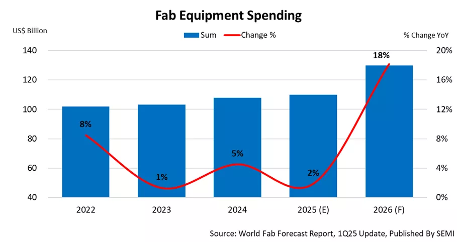
MILPITAS, Calif. — March 25, 2025 — Global fab equipment spending for front-end facilities in 2025 is anticipated to increase by 2% year-over-year (YoY) to $110 billion, marking the sixth consecutive year of growth since 2020, SEMI announced today in its latest quarterly World Fab Forecast report. 

Fab equipment spending is projected to rise by 18% in the following year, reaching $130 billion. This growth in investment is driven not only by demand in the high-performance computing (HPC) and memory sectors to support data center expansions, but also by the increasing integration of artificial intelligence (AI), which is driving up the silicon content required for edge devices.

SEMI“The global semiconductor industry’s investments in fab equipment have been edging up for six straight years, and spending is poised to see a strong 18% increase in 2026 as production ramps to meet booming AI-related chip demand,” said Ajit Manocha, SEMI President and CEO. “This forecasted capex growth signals an urgent need for intensified workforce development initiatives throughout 2025 and 2026 to deliver skilled workers necessary for the approximately 50 new fabs expected to come online during these two years.” 
FES

Logic & Micro Segment Lead Semiconductor Industry Expansion

The Logic & Micro segment is anticipated to be a key driver of growth in fab investments. This growth is primarily fueled by investments in cutting-edge technologies, such as 2-nanometer process and backside power delivery technology, which are expected to enter production by 2026. The Logic & Micro segment is projected to see an 11% increase in investments, reaching $52 billion in 2025, followed by a 14% increase to $59 billion in 2026.

Overall Memory segment spending is expected to grow steadily the next two years, increasing by 2% to reach $32 billion by 2025, with an even stronger growth forecast of 27% in 2026. Investments in the DRAM segment are projected to decline by 6% year-over-year, totaling $21 billion in 2025, but are anticipated to rebound with a 19% increase to $25 billion in 2026. Conversely, NAND segment spending is expected to recover significantly, rising by 54% year-over-year to $10 billion in 2025, and further increasing by 47% to $15 billion in 2026. 

China Continues to Lead in Regional Fab Equipment Spending 

Despite a decline from a peak of $50 billion in 2024, China is expected to maintain its position as the leader in global semiconductor equipment spending, with projections of $38 billion in 2025 representing a 24% year-over-year decrease. By 2026, spending is forecast to decline further 5% year-over-year to $36 billion.

With the growing penetration of AI technology driving higher memory adoption, Korean chipmakers are planning to invest more in equipment for capacity expansion and technology upgrades, which is expected to position the region as the second highest spending through 2026. Korean investment is forecasted to grow by 29% to $21.5 billion in 2025 and by 26% to $27 billion in 2026.

Taiwan is set to secure third place in spending as its chipmakers aim to enhance their leadership in advanced technology and production capabilities. Taiwan is projected to spend $21 billion in 2025 and $24.5 billion in 2026 to meet the growing demand for AI applications across cloud services and edge devices.

The Americas region ranks fourth, with expected spending of $14 billion in 2025 and $20 billion in 2026. Japan, Europe and the Middle East, and Southeast Asia follow in investments, projected to spend $14 billion, $9 billion, and $4 billion in 2025, and $11 billion, $7 billion, and $4 billion in 2026, respectively.

The latest update of the SEMI World Fab Forecast report, published in March, lists more than 1,500 facilities and lines globally, including 156 facilities and lines with various probabilities expected to start operation in 2025 or later.  

Download a sample of the SEMI World Fab Forecast report.

For details about SEMI reports on other semiconductor sectors, visit SEMI Market Data or contact the SEMI Market Intelligence Team (MIT) at [email protected].

About SEMI

SEMI® is the global industry association connecting over 3,000 member companies and 1.5 million professionals worldwide across the semiconductor and electronics design and manufacturing supply chain. We accelerate member collaboration on solutions to top industry challenges through Advocacy, Workforce Development, Sustainability, Supply Chain Management and other programs. Our SEMICON® expositions and events, technology communities, standards and market intelligence help advance our members’ business growth and innovations in design, devices, equipment, materials, services and software, enabling smarter, faster, more secure electronics. Visit www.semi.org, contact a regional office, and connect with SEMI on LinkedIn and X to learn more.  

Association Contacts

Christian G. Dieseldorff/SEMI US
Phone: 1.408.943.7940
Email: [email protected]  

Chih-Wen Liu/SEMI Taiwan
Phone: 886.3.560.1777
Email: [email protected]

Samer Bahou/SEMI Corporate 
Phone: 1.408.943.7870
Email: [email protected]

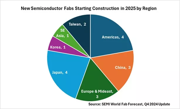
MILPITAS, Calif. — January 7, 2025 — The semiconductor industry is expected to start 18 new fab construction projects in 2025*, according to SEMI's latest quarterly World Fab Forecast report. The new projects include three 200mm and fifteen 300mm facilities, the majority of which are expected to begin operations from 2026 to 2027. 

SEMIIn 2025, the Americas and Japan are the leading regions with four projects each. The China and Europe & Middle East regions are each tied for third place with three planned construction projects. Taiwan has two planned projects, while Korea and Southeast Asia have one project each for 2025.

 

New semiconductor fabs starting construction


“The semiconductor industry has reached a pivotal juncture, with investments driving both leading-edge and mainstream technologies to meet evolving global demands,” said Ajit Manocha, SEMI President and CEO. “Generative AI and high-performance computing are fueling advancements in the leading-edge logic and memory segments, while mainstream nodes continue to underpin critical applications in automotive, IoT and power electronics. The construction of 18 new semiconductor fabs set to begin in 2025 demonstrates the industry’s commitment to support innovation and significant economic growth.”

Covering 2023 to 2025, the 4Q 2024 edition of World Fab Forecast report shows that the global semiconductor industry plans to begin operation of 97 new high-volume fabs. This includes 48 projects in 2024 and 32 projects set to launch in 2025, with wafer sizes ranging from 300mm to 50mm.

Advanced Nodes Lead Semiconductor Industry Expansion 

Semiconductor capacity is projected to further accelerate, with a 6.6% yearly growth rate forecast to total 33.6 million wafers per month (wpm)** for 2025. This expansion will be primarily driven by leading-edge logic technologies in high-performance computing (HPC) applications and the increasing penetration of generative AI in edge devices.

The semiconductor industry is intensifying efforts to build advanced computing capabilities, responding to the escalating computational demands of large language models (LLMs). Chip manufacturers are aggressively expanding advanced node capacities (7nm and below), which are expected to see an industry-leading 16% yearly growth rate for an increase of more than 300,000 wpm to total 2.2 million wpm in 2025.

Boosted by China’s chip self-sufficiency strategy and expected demand from automotive and IoT applications, mainstream nodes (8nm~45nm) are predicted to add another 6% capacity, surpassing the 15 million wpm milestone in 2025.

Mature technology nodes (50nm and above) are experiencing a more conservative expansion, reflecting the market’s slow recovery and low utilization rates. This segment is expected to grow 5%, reaching 14 million wpm in 2025.

Foundry Segment Continues Strong Capacity Growth 

Foundry suppliers are expected to remain the leaders in semiconductor equipment purchases. The Foundry segment is projected to increase capacity by 10.9% year-over-year, rising from 11.3 million wpm in 2024 to a record 12.6 million wpm in 2025.

The overall memory segment shows a measured capacity expansion, with modest growth of 3.5% in 2024 and 2.9% in 2025. However, strong generative AI demand is driving significant changes in memory markets. High-bandwidth memory (HBM) is experiencing a notable surge, creating divergent capacity growth trends between the DRAM and NAND flash segments.

The DRAM segment is expected to maintain robust growth, projecting approximately a 7% year-over-year increase to 4.5 million wpm in 2025. Conversely, the installed capacity for 3D NAND is anticipated to grow 5%, reaching 3.7 million wpm in the same period.

The latest update of the SEMI World Fab Forecast report, published in December 2024, lists more than 1,500 facilities and lines globally, including 180 volume facilities and lines with various probabilities expected to start operation in 2025 or later.  

Download a sample of the SEMI World Fab Forecast report.

For details about SEMI reports on other semiconductor sectors, visit SEMI Market Intelligence or contact us at [email protected].

*The fab count does not include research and development (R&D) lines

**200mm equivalent

About SEMI

SEMI® is the global industry association connecting over 3,000 member companies and 1.5 million professionals worldwide across the semiconductor and electronics design and manufacturing supply chain. We accelerate member collaboration on solutions to top industry challenges through Advocacy, Workforce Development, Sustainability, Supply Chain Management and other programs. Our SEMICON® expositions and events, technology communities, standards and market intelligence help advance our members’ business growth and innovations in design, devices, equipment, materials, services and software, enabling smarter, faster, more secure electronics. Visit www.semi.org, contact a regional office, and connect with SEMI on LinkedIn and X to learn more.  

Association Contacts

Samer Bahou/SEMI Corporate
Phone: 1.408.943.7870
Email: [email protected] 

Christian G. Dieseldorff/SEMI US
Phone: 1.408.943.7940
Email: [email protected]  

Chih-Wen Liu/SEMI Taiwan
Phone: 886.3.560.1777
Email: [email protected]

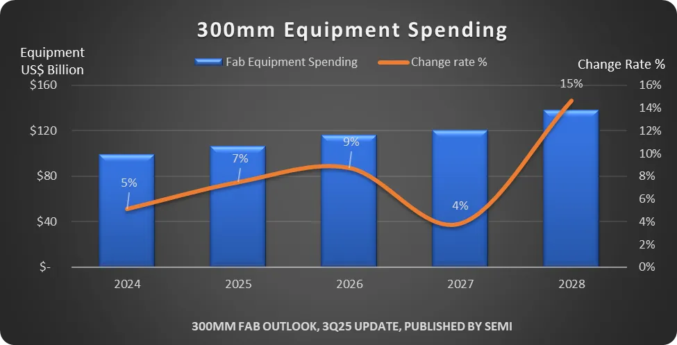
MILPITAS, Calif. — September 26, 2024 — Global spending on 300mm fab equipment is expected to reach a record US$400 billion from 2025 to 2027, SEMI highlighted today in its quarterly 300mm Fab Outlook Report to 2027 report. The robust spending is being driven by the regionalization of semiconductor fabs and the increasing demand for artificial intelligence (AI) chips used in data centers and edge devices.

SEMI LogoWorldwide, 300mm fab equipment spending is projected to grow by 4% to US$99.3 billion in 2024, and further increase by 24% to US$123.2 billion in 2025, surpassing the US$100 billion level for the first time. Spending is forecast to experience 11% growth to US$136.2 billion in 2026 followed by a 3% increase to US$140.8 billion in 2027.
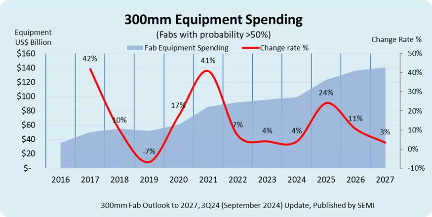
“The magnitude of the expected ramp of global 300mm fab equipment spending in 2025 sets the stage for a record-setting three-year period of semiconductor manufacturing investments,” said Ajit Manocha, SEMI President and CEO. “The world’s ubiquitous need for chips is boosting spending on equipment for both leading-edge technologies addressing AI applications and mature technologies driven by automotive and IoT applications.”


300mm Equipment Spending


Regional Growth

China is projected to maintain its position as the top spending region on 300mm equipment globally until 2027, investing over US$100 billion in the next three years driven by its national self-sufficiency policies. However, spending is anticipated to gradually decrease from a peak of US$45 billion in 2024 to US$31 billion by 2027.

Korea is projected to rank second and invest US$81 billion in the next three years to further its dominance in memory segments including DRAM, high-bandwidth memory (HBM), and 3D NAND Flash. Taiwan is forecast to spend US$75 billion on 300mm equipment over the next three years, ranking third as the region’s chipmakers build some new fabs overseas. Leading-edge logic below 3nm is the primary driver of Taiwan fab investments.

The Americas is projected to invest US$63 billion from 2025 to 2027, while Japan, Europe & Mideast, and SE Asia are expected to spend US$32 billion, US$27 billion, and US$13 billion, respectively, over the three-year period. Notably, these regions are anticipated to more than double their equipment investment in 2027 compared to 2024 due to policy incentives earmarked to alleviate concerns on the supply of crucial semiconductors.

Segment Growth

Foundry equipment spending is projected to reach approximately US$230 billion between 2025 and 2027, fueled by investments in sub-3nm cutting-edge nodes as well as continued spending on mature nodes. Investment in 2nm logic processes and development of key technologies at 2nm, such as gate-all-around (GAA) transistor structure and back-side power delivery technology, is crucial to meet future high-performance and energy-efficient computing needs, particularly for AI applications. Cost-effective 22nm and 28nm processes are expected to see growth due to increasing demand for automotive electronics and IoT applications.

The Logic and Micro segment is projected to spearhead the equipment spending expansion over the next three years, with an anticipated total investment of US$173 billion. Memory comes in second, expected to contribute over US$120 billion in spending during the same period, marking the beginning of another segment growth cycle. Within Memory, investment in DRAM-related equipment is projected to surpass US$75 billion, while investment in 3D NAND is expected to reach US$45 billion.

The Power-related segment ranks third, with an expected investment of over US$30 billion over the next three years, including around US$14 billion for compound semiconductor projects. The Analog and Mixed-signal segment is projected to reach US$23 billion during the same period followed by Opto/Sensors at US$12.8 billion.

Part of the SEMI Fab Forecast database, the SEMI 300mm Fab Outlook Report to 2027 report lists 420 facilities and lines globally, including 79 high-probability facilities expected to start operation during the four years beginning in 2024. The report reflects 169 updates and nine new fabs/lines projects since its last publication in June 2024.  

For more information on the report or to subscribe to SEMI market data, visit SEMI Market Data or contact the SEMI Market Intelligence Team (MIT) at [email protected].

About SEMI

SEMI® is the global industry association connecting over 3,000 member companies and 1.5 million professionals worldwide across the semiconductor and electronics design and manufacturing supply chain. We accelerate member collaboration on solutions to top industry challenges through Advocacy, Workforce Development, Sustainability, Supply Chain Management and other programs. Our SEMICON® expositions and events, technology communities, standards and market intelligence help advance our members’ business growth and innovations in design, devices, equipment, materials, services and software, enabling smarter, faster, more secure electronics. Visit www.semi.org, contact a regional office, and connect with SEMI on LinkedIn and X to learn more.

Association Contacts

Samer Bahou/SEMI Communications
Phone: 1.408.943.7870
Email: [email protected] 

Christian G. Dieseldorff/SEMI US
Phone: 1.408.943.7940
Email: [email protected]  

Chih-Wen Liu/SEMI Taiwan
Phone: 886.3.560.1777
Email: [email protected]