downloadGroupGroupnoun_press release_995423_000000 copyGroupnoun_Feed_96767_000000Group 19noun_pictures_1817522_000000Member company iconResource item iconStore item iconGroup 19Group 19noun_Photo_2085192_000000 Copynoun_presentation_2096081_000000Group 19Group Copy 7noun_webinar_692730_000000Path
Skip to main content
Default Banner Image

Fab

Rogue Valley Microdevices (RVM), a U.S.-based pure-play MEMS foundry, today announced the launch of its foundry-flexible MEMS Design Services, expanding its ability to support customers from early concept through production-ready device design.

This new capability allows customers to work with RVM as a design partner independent of fabrication location. Customers can develop manufacturable MEMS devices with RVM and then choose to fabricate at the foundry that best aligns with their technical requirements, capacity needs, and supply chain strategy.

RVM offers three flexible engagement models:
• Design – MEMS device design, modeling, and layout development
• Design & Technology Transfer – Design with structured transfer to a customer-selected foundry
• Design & Fabricate – Integrated design-to-manufacturing within RVM’s MEMS foundry

This approach gives customers greater control over development risk, cost, and supply chain resilience while ensuring designs are grounded in real fabrication processes from the start.

To lead this initiative, Rogue Valley Microdevices has appointed Scott Rauscher, PhD, a MEMS engineering leader with nearly two decades of experience spanning U.S. government research, defense programs, and commercial technology development.

MEMS Design Services at Rogue Valley Microdevices

The addition of design services reflects growing demand for deeper collaboration during device development and increased flexibility in selecting manufacturing partners.

“Many of our customers are pushing the boundaries of MEMS performance and integration, and that requires close collaboration between design and manufacturing,” said Jessica Gomez, CEO of Rogue Valley Microdevices. “By adding design services alongside our fabrication capabilities, we help customers accelerate development, optimize device performance, and move more efficiently from concept to commercialization. Scott Rauscher’s experience across design, modeling, and microfabrication makes him the ideal leader to build this capability.”

RVM’s Design Services support customers across key areas of MEMS development, including:
• MEMS device design and layout development
• Implementation of design rule checks and layout standards
• Design-of-experiment (DOE) array creation
• Integration of process monitors for lithography, etch, and thin film validation
• Process flow development and refinement for manufacturability

RVM’s engineering team works closely with customers to align device design with proven fabrication methods, reducing iteration cycles and improving first-pass success.
In parallel, Rogue Valley Microdevices is developing more automated design workflows using industry tools such as L-Edit and K-Layout, while advancing toward a formal Process Design Kit (PDK) to further streamline collaboration and accelerate development timelines.

Scott Rauscher Joins Rogue Valley Microdevices Team

Scott Rauscher brings extensive experience in MEMS design and technology development across both government and industry. Most recently at L3Harris Technologies, he led process architecture and technology strategy while managing a microfabrication and design engineering team. In that role, he developed critical device technology and helped grow it into a portfolio exceeding $80 million.

His career also includes leadership roles at the Naval Surface Warfare Center and the U.S. Army Research Laboratory, where he served as a MEMS device inventor and microfabrication lead. Rauscher holds more than ten patents issued and pending and has been active in industry and research organizations, including the Florida Semiconductor Institute, the MMEC consortium’s Quantum Working Group, and national semiconductor infrastructure initiatives.

“Rogue Valley Microdevices is uniquely positioned to help customers bridge the gap between innovative device concepts and manufacturable products,” said Dr. Scott Rauscher, Chief Innovation Officer, Rogue Valley Microdevices. “With the new Palm Bay facility coming online and the addition of integrated design services, we have an opportunity to build a collaborative environment where device engineers can work closely with the fab to accelerate development and scale promising technologies into production.”

The launch of Design Services marks another step forward for Rogue Valley Microdevices as it prepares to open its Palm Bay facility and expand its U.S.-based manufacturing capabilities. Together with the company’s established operations in Medford, Oregon, the new fab will strengthen domestic MEMS production capacity while providing customers with greater supply chain resilience and advanced wafer services.

To learn more about RVM’s Design Services, please contact: [email protected]

About Rogue Valley Microdevices

Rogue Valley Microdevices (RVM) is a U.S.-based pure-play MEMS foundry providing integrated design services, MEMS manufacturing, and wafer services, enabling customers to move efficiently from concept to scalable manufacturing. RVM supports the full MEMS development lifecycle, from device design and process development to volume manufacturing. By aligning design with proven fabrication processes from the outset, RVM helps reduce development risk and accelerate time to market.
With operations in Medford, Oregon, and a new 300 mm MEMS-capable facility in Palm Bay, Florida, RVM supports applications across MEMS, sensors, photonics, and specialty post-CMOS technologies. The company serves customers in industries including healthcare and biotech, industrial sensing, aerospace and defense, communications, and advanced electronics. By combining collaborative design expertise, flexible process development, and domestic manufacturing capability, RVM delivers a transparent, customer-focused approach that strengthens supply chain resilience and provides a clear path from innovation to volume manufacturing.
For more information, visit www.roguevalleymicro.com

Media Contact:
Maria Doyle
Doyle Strategic Communications (for Rogue Valley Microdevices)
781-964-3536
[email protected]

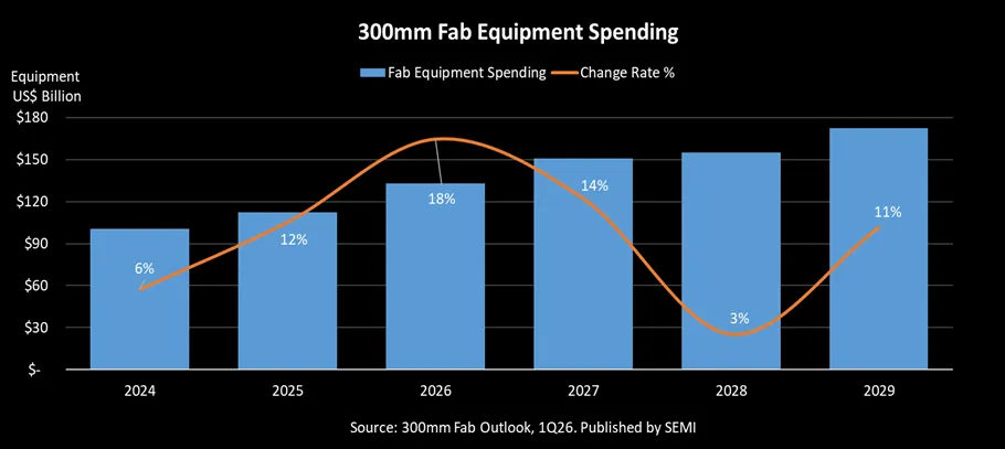
MILPITAS, Calif. – April 1, 2026 – Worldwide 300mm fab equipment spending is expected to increase 18% to $133 billion in 2026 and 14% to $151 billion in 2027, SEMI reported today in its latest 300mm Fab Outlook. This strong growth reflects surging AI chip demand for data centers and edge devices, as well as the growing commitment to semiconductor self-sufficiency across key regions through localized industrial ecosystems and supply chain restructuring.

Looking further out, the report projects investment will continue to increase 3% to $155 billion in 2028 and another 11% to $172 billion in 2029, respectively.

“AI is resetting the scale of semiconductor manufacturing investment,” said Ajit Manocha, President and CEO of SEMI. “With global 300mm fab equipment spending projected to exceed $150 billion in 2027 for the first time, the industry is making historic, sustained commitments to the advanced capacity and resilient supply chains needed to power the AI era.”


Segment Growth

The Logic & Micro segment is expected to spearhead equipment expansion with $228 billion in total investments from 2027 to 2029 mainly due to strong foundry sector demand, driven by sub-2nm cutting-edge capacity investments. Advanced node technology is essential to enhance chip performance and power efficiency to meet rigorous chip design requirements for various AI applications. More advanced node technology is expected to enter volume production from 2027 to 2029. Additionally, AI performance improvements are anticipated to drive massive growth in various edge AI devices. Beyond advanced nodes, demand across all nodes and various electronics devices is anticipated to grow moderately, supporting investment in mature nodes as well.

The memory segment is projected to rank second in equipment spending, totaling $175 billion from 2027 to 2029. This period marks the start of a new growth cycle for the segment. Within the memory category, DRAM equipment spending is expected to reach $111 billion cumulatively from 2027 to 2029, while 3D NAND equipment spending is estimated to be $62 billion during the same time frame. 

The demand for memory has significantly increased due to AI training and inference. AI training has notably driven up the demand for High Bandwidth Memory (HBM), while model inference has created substantial demand for storage capacity, thus boosting the growth of NAND Flash applications in data centers. This strong demand has led to sustained high levels of investment in the memory supply chain over the near and long term, helping to cushion potential downturns from traditional memory cycle fluctuations.

Regional Investment Trends

Global 300mm fab equipment investment is expected to remain broadly distributed across the major semiconductor manufacturing regions from 2027 to 2029, reflecting a mix of advanced-node expansion, memory capacity additions, and policy-supported supply chain localization. China, Taiwan, Korea, and the Americas are each expected to see substantial levels of spending during the period, while Japan, Europe & Middle East, and Southeast Asia also continue to expand investment from a smaller base. 

In China, investment is expected to remain supported by ongoing domestic capacity expansion and national initiatives aimed at strengthening semiconductor manufacturing capabilities. In the Taiwan region, spending is projected to be driven primarily by continued expansion of leading-edge foundry capacity, including 2nm and sub-2nm technologies. Korea’s investment outlook remains closely tied to the memory sector, where AI-related demand is supporting another cycle of capacity and technology upgrades. In the Americas, spending is expected to be underpinned by advanced process expansion and broader efforts to strengthen domestic manufacturing ecosystems. 

Japan, Europe & Middle East, and Southeast Asia are also expected to post meaningful growth through 2029. In these regions, equipment investment is supported by a combination of government incentives, supply chain resilience strategies, and targeted efforts to expand semiconductor manufacturing capacity.

Part of the SEMI Fab Forecast database, the SEMI 300mm Fab Outlook lists 404 facilities and lines globally. The report reflects 198 updates and 9 new fabs/lines projects since its last publication in December 2025. 

For more information on the report or to subscribe, please contact the SEMI Market Intelligence Team at [email protected]. Details on SEMI market data are available at SEMI Market Intelligence.  

Follow SEMI 

About SEMI

SEMI® is the global industry association connecting over 3,000 member companies and 1.5 million professionals worldwide across the semiconductor and electronics design and manufacturing supply chain. We accelerate member collaboration on solutions to top industry challenges through Advocacy, Workforce Development, Sustainability, Supply Chain Management and other programs. Our SEMICON® expositions and events, technology communities, standards and market intelligence help advance our members’ business growth and innovations in design, devices, equipment, materials, services and software, enabling smarter, faster, more secure electronics. Visit www.semi.org, contact a regional office, and connect with SEMI on LinkedIn and X to learn more

High-performance connectivity software delivers structured, high-volume equipment data required by tier-one fabs and advanced packaging facilities ahead of the expected mid-2026 SEMI standards update

POITIERS, March 25, 2026 – Agileo Automation, a leading provider of control and connectivity solutions for global semiconductor manufacturing, today unveils Agil'EDA, a new software solution implementing Equipment Data Acquisition (EDA), a set of SEMI standards also known as Interface A, to enable semiconductor equipment manufacturers to meet the evolving high-performance connectivity requirements of tier-one fabs and advanced packaging facilities.

As semiconductor manufacturing moves towards higher levels of automation and data-driven optimization, fab owners increasingly require EDA alongside traditional SECS/GEM connectivity from semiconductor OEMs for their production tools. Agil'EDA addresses this by separating the control flow from the data flow, ensuring that structured, high-frequency data collection does not interfere with critical equipment operations.
Designed for long-term deployment, Agil'EDA fully supports the widely used EDA Freeze 2 (SOAP/XML) and is architected for the transition to Freeze 3 (gRPC/protocol buffers). This next-generation standard offers significantly higher data throughput and reduced latency. Agileo has already successfully tested and validated its EDA Freeze 3 implementation at SEMI’s North America Standards Fall Meetings in November 2024 in Milpitas, California. SEMI’s EDA Freeze 3 standards suite is expected to be released mid-2026.

Complementing the SECS/GEM standards used to control equipment behavior, Agil’EDA incorporates robust cybersecurity features such as authentication and encrypted communications. The product is available as a stand-alone solution for any existing equipment software using a platform-independent gRPC application programming interface (API) to communicate with it or as a pre-integrated component within Agileo’s A²ECF-SEMI framework. When used with Agil'GEM and Agil'GEM300, it provides a comprehensive connectivity solution that significantly reduces time to market for OEMs.

"With the growing demand for data to improve yield in tier-one fabs, as well as in Advanced Packaging and 3D integration, EDA is no longer optional. It is becoming a mandatory requirement for equipment entering the world's most advanced fabs," explains Marc Engel, chief executive officer of Agileo Automation. "The key value we deliver for OEMs is a fast and easy adoption path for a seamless EDA architecture that delivers compliant production machines to global fab customers. By providing a future-proof architecture ready for Freeze 3, which will significantly increase performance, we address OEMs’ current needs while preparing them for the evolving requirements of semiconductor manufacturing, including AI-driven process control."

- ends -

About Agileo Automation
Agileo Automation is a trusted partner for equipment manufacturers, helping them build smarter, automated, and more connected machines that integrate seamlessly into advanced semiconductor fabs. Founded in 2010 in Poitiers, France, Agileo helps OEMs with control, communication, data acquisition, and testing across their tools through proven software and expert support. Its flagship A²ECF-SEMI framework provides a solid foundation for developing equipment controllers fully aligned with SEMI SECS/GEM, GEM300, and EDA standards. As an active member of SEMI and the OPC Foundation, Agileo Automation contributes directly to shaping the standards that drive manufacturing. For more information, please visit our website or follow us on LinkedIn.

Dresden, Germany, March 24, 2026 – As semiconductor manufacturing continues to expand in China, reliable and efficient environmental technologies are becoming increasingly important for stable and sustainable fab operation. DAS Environmental Experts presents its SALIX wet scrubber product family, a series of high-efficiency point-of-use systems designed for the treatment of waste gases from wet chemical processes in semiconductor manufacturing.

SALIX systems are engineered to ensure high removal efficiency and stable operation in demanding semiconductor production environments. SALIX reliably removes substances such as IPA, ammonia and hydrofluoric acid (HF) from waste gas streams of modern single wafer clean systems – a key contribution to safe and sustainable semiconductor manufacturing. In addition, the technology removes particles, salts and droplets from the processed gas stream. The robust system design supports high uptime and long maintenance intervals, contributing to reliable fab operation.

A key advantage of the SALIX product family is its flexible portfolio. SALIX products are among the smallest and most compact systems on the market and are suitable for both new fabs and retrofit applications in existing fabs. DAS Environmental Experts offers the technology in four different products, providing semiconductor manufacturers with a wide range of configuration options:

• NEW: SALIX – the latest release with improved performance and optimized system operation
• SALIX MINI – a compact two-stage system for space-constrained installations
• NEW: SALIX MICRO [SR1.1]– a highly compact configuration with pre-scrubber section for flexible integration

This structured product portfolio enables customers to select the most suitable system according to process requirements, fab layout and integration needs. The availability of multiple system variants within one technology platform provides semiconductor manufacturers with excellent flexibility in system selection and plant design.

SALIX systems are designed for compatibility with all common process tools and can be adapted to a wide range of wet chemical applications. Their compact design and flexible configuration support efficient integration into modern fabs, helping manufacturers optimize both environmental performance and operational efficiency.

The SALIX product family will be presented during SEMICON China 2026 (March 25–27, Shanghai New International Expo Centre). Interested visitors can learn more about the technology and its applications at the DAS Environmental Experts booth (Booth N2 | 2619).

With more than three decades of experience in environmental technology for the semiconductor industry, DAS Environmental Experts continues to support chip manufacturers worldwide with solutions that combine high process reliability, efficient emission treatment and long-term operational stability.

About the Company
DAS Environmental Experts Group (DAS Group), headquartered in Dresden, Germany, was founded in 1991 and is now a global organization with subsidiaries on three continents and more than 950 employees worldwide. Over the past three decades, DAS Group has become one of the leading technology and equipment providers for waste gas abatement solutions with a focus on semiconductor industry.
In addition, DAS Group develops advanced process and system solutions for industrial water treatment, with extensive expertise in the recycling and reuse of wastewater from the semiconductor industry.
DAS solutions are engineered to meet the stringent purity requirements of semiconductor manufacturing, helping clients comply with global environmental standards.

Location: Richardson, Texas

Modus Test, a leader in advanced test socket testing solutions and performance validation, and yieldWerx, a semiconductor data and yield analytics platform, today announced a strategic partnership to help close the gap between test hardware and yield intelligence. The collaboration combines Modus Test’s high-performance socket test technology with yieldWerx’s enterprise-scale yield management platform to provide manufacturers with direct visibility into the relationship between socket health and device performance.

The partnership addresses a long-standing disconnect between test execution and data analytics in high- volume manufacturing. Degraded, misaligned, or worn sockets can introduce false failures or escapes without clear root-cause identification. By integrating hardware performance data with yield analytics, manufacturers can better distinguish contact-related artifacts from true silicon failures.
Through this partnership, customers can now:
• Monitor and trend socket performance across testers, sites, and handlers
• Correlate device failures to specific sockets, test cells, or contact events
• Identify unnecessary device rejects caused by socket degradation
• Detect potential escapes where devices pass due to intermittent contact issues
• Optimize preventive maintenance cycles using data-driven insights

By integrating Modus Test equipment data with yieldWerx’s wafer-, lot-, and device-level analytics, manufacturers gain the ability to separate true device behavior from test interface variability, improving confidence in test outcomes and accelerating root-cause resolution.

About yieldWerx
yieldWerx provides a semiconductor yield management platform that enables manufacturers to collect, analyze, and act on production data across the manufacturing lifecycle. The platform consolidates data from wafer fabrication through final test, delivering visibility into product quality, process performance, and yield improvement opportunities.

About ModusTest
Modus Test, LLC was founded on the idea that there are creative ways to improve results by combining innovation with the best-known methods in test design and manufacturing. Providing innovative test solutions includes the MPT series of parametric tests, systems, and accessories. Modus Test has a global presence and the capability to support customers in all the IC development centers and high-volume manufacturing sites around the world. See for yourself how combining innovation with best-known methods can improve your results.

Statements from Leadership
“yieldWerx was built to unify disparate manufacturing data into actionable yield intelligence,” said Aftkhar Aslam, CEO of yieldWerx. “Valuable data exists across testers, handlers, sockets, MES systems, and inspection tools, but it often remains siloed. Our platform connects these domains into a unified analytical framework that enables faster, data-driven decisions that reduce costs.”

“This partnership represents an important step forward in bringing greater transparency and intelligence to semiconductor test,” said Jesse Ko, COO of Modus Test. “Modus Test’s high-performance socket validation solutions, combined with yieldWerx’s powerful analytics platform, create a closed-loop ecosystem where hardware performance and yield outcomes are fully correlated. Together, we are enabling a smarter, more adaptive test environment.”

For further information, please visit https://www.yieldWerx.com or https://www.ModusTest.org.

LOS ANGELES (Jan. 28, 2026) – EMASS, a Nanoveu subsidiary specializing in next-generation semiconductor technology, today announced the successful tape-out of its 16nm ECS-DoT system-on-chip (SoC). The device has entered fabrication at TSMC, marking the transition of EMASS’s next-generation ultra-low-power edge AI architecture from final design into production silicon.

The 16nm ECS-DoT represents a process-node and architectural scaling of EMASS’s proven 22nm ECS-DoT platform, increasing compute density, memory bandwidth and system integration while preserving the ultra-low-power design principles that define the ECS-DoT family. The move to 16nm enables higher logic density and tighter subsystem integration, supporting more complex always-on workloads within the same constrained power envelopes required at the extreme edge.

The current 22nm ECS-DoT SoC is EMASS’s commercially available platform and is actively being designed into customer products today, including applications across wearables, industrial sensors, asset tracking, smart infrastructure and other always-on edge use cases. This in-market traction provides a production-proven foundation for the 16nm ECS-DoT, enabling customers to scale existing designs to higher performance and integration without changing software workflows or system architecture.

By transitioning to 16nm, EMASS is able to expand on-chip SRAM capacity, integrate additional system-level functions and enhance AI and DSP acceleration without altering the underlying programming model or software toolchain. Wireless connectivity, dedicated AI accelerators and fine-grained power-management blocks are tightly coupled within a single SoC, reducing reliance on external components and enabling continuous, low-latency operation in battery-powered and energy-harvesting edge devices.

“Reaching tape-out confirms that our ultra-low-power edge AI approach scales cleanly to more advanced nodes,” shared Mark Goranson, CEO of EMASS. “The 16nm ECS-DoT is not just a faster or smaller device. It's proof that always-on intelligence can move into more demanding applications without breaking power, cost or system constraints.”

The 16nm ECS-DoT increases system capability while reducing external component dependency, allowing developers to build more intelligent edge devices with fewer tradeoffs. Key capabilities include:

Fully integrated BLE subsystem — Eliminates the need for external wireless ICs, reducing board area, bill-of-materials cost and design complexity.
Expanded on-chip memory — Supports larger AI models and higher-throughput workloads while minimizing off-chip memory access for improved efficiency.

Adaptive fine-grained power-management architecture — Optimizes energy use for always-on, battery-powered and energy-harvesting applications.

Dedicated object-detection accelerator — Offloads vision workloads to increase throughput and reduce inference latency for edge vision use cases.

Integrated floating-point unit (FP16/FP32) — Accelerates DSP and mixed-precision AI workflows while simplifying developer toolchains and code migration.

Despite the move to a 16nm process node, the ECS-DoT architecture maintains full software compatibility across generations. Developers can migrate applications between the 22nm and 16nm devices with minimal changes, preserving existing investments while unlocking additional performance and system headroom. This continuity allows customers to scale functionality and intelligence over time without redesigning platforms or toolchains, accelerating time-to-market for next-generation edge products.

The tape-out of the 16nm ECS-DoT further strengthens EMASS’s “Atoms-to-Apps” development philosophy, aligning application needs, algorithm design and silicon implementation into a cohesive system-level approach.

“Tape-out validates years of architectural decisions,” said Dr. Mohamed Sabry, founder and CTO of EMASS. “With the 16nm ECS-DoT now in fabrication, we’ve demonstrated that our architecture can deliver higher integration and capability without sacrificing energy efficiency. This milestone positions EMASS to support a broader range of always-on edge AI applications while staying true to the fundamentals that define our platform.”

###

About EMASS
EMASS – a subsidiary of Nanoveu Ltd (ASX: NVU) – is an advanced semiconductor company specializing in ultra-low-power AI system-on-chip (SoC) solutions for edge computing. The company's flagship ECS-DoT chip delivers high-performance AI processing for vision, audio, and sensor data directly on-device, maximizing energy efficiency through its RISC-V architecture and non-volatile memory technologies. This always-on intelligence solution is optimized for power- and space-constrained applications including drones, wearables, healthcare devices and industrial IoT systems. For more information, visit nanoveu.com/emass.

About Nanoveu
Nanoveu is a listed company advancing human–machine experiences at the edge through a portfolio that spans ultra-low-power AI and glasses-free 3D technologies. Its subsidiary EMASS designs advanced system-on-chip (SoC) solutions that deliver efficient, scalable on-device AI for smart devices, IoT applications and 3D content transformation – enhancing Nanoveu’s reach across rapidly growing AI, edge computing and 3D content markets. EyeFly3D™ is Nanoveu’s end-to-end platform for glasses-free 3D, uniting proprietary screen technology with sophisticated content processing software and, now, EMASS’s ultra-low-power SoC to bring immersive 3D to a wide range of devices and industries. The Company also develops and markets an advanced range of self-disinfecting and hydrophobic films and coatings under the Nanoshield™ brand, designed for applications including large-scale CSP and photovoltaic solar installations. Together, Nanoveu’s businesses deliver practical innovation that makes devices smarter, environments safer and experiences more immersive.

Media Contact
Zach Hynoski
[email protected]
+1 (732) 581-6237

Oxford Instruments, a leading provider of advanced plasma processing solutions, today announced a plasma equipment supply agreement with Applied Optoelectronics Inc. (AOI) (Nasdaq: AAOI), a leading provider of advanced optical and hybrid fibre-coaxial networking products that power the internet, for several etch and deposition cluster systems at their facility in Sugar Land, Texas.

The agreement will support AOI’s transformative expansion and technological advancements in indium phosphide (InP) for optoelectronic device manufacturing, as the company rapidly scales to increase production capacity within the U.S.

As AOI undergoes a significant growth phase, the company is upgrading its production capabilities to meet increasing demand for high-performance InP optoelectronic devices. Oxford Instruments’ advanced plasma etch and deposition processing systems will play a key role in this transformation by supporting AOI with fully automated 3-4-6-inch capable production systems for InP processes.

“AOI is expanding its U.S. manufacturing capacity in Texas to support demand for our optical transceivers in AI datacentres, and key suppliers like Oxford Instruments will help us continue to upgrade our fully automated production line,” said Fred Chang, Senior Vice President and North American General Manager at AOI. “With our combined technology, we can speed the processing of multiple wafer sizes, ranging from 3 to 6 inches, while improving overall quality and reducing costs.”

“AOI has been a valued long-term partner, and we are thrilled to have earned their trust as the chosen supplier for their production expansion and technology upgrades. Our unique high-temperature Electrostatic Chuck (ESC) design, which enables advanced processing capabilities, was a key factor in their decision. AOI also conducted an extensive vendor qualification process, including a visit to our brand-new purpose-built manufacturing facility in Bristol, UK, where we received high praise for our technology and production capabilities,” said Emiel Thijssen, Vice President of Sales and Business Development USA, Oxford Instruments Plasma Technology. “We are also investing significantly to ensure we continue to deliver world-class service capability in the Texas region, focusing on the availability of spares and expanding our field service and process engineering teams, to support the rapid expansion of leading manufacturers in the region such as AOI.”

###


For media enquiries, please contact:
Grant Baldwin, Head of Marketing
Oxford Instruments Plasma Technology
E: [email protected]
About Oxford Instruments plc
Oxford Instruments provides academic and commercial organisations worldwide with market-leading scientific technology and expertise across its key market segments: Materials Analysis, Healthcare & Life Science and Semiconductors. Innovation is the driving force behind Oxford Instruments' growth and success, supporting its core purpose to accelerate the breakthroughs that create a brighter future for our world. The vigorous search for new ways to make our world greener, healthier and more productive is driving unprecedented levels of R&D investment in new materials and techniques to support productivity and decarbonisation worldwide, creating a significant opportunity for Oxford Instruments to grow.

Oxford Instruments holds a unique position to anticipate global drivers and connect academic researchers with commercial applications engineers, acting as a catalyst that powers real world progress. Founded in 1959 as the first technology business to be spun out from Oxford University, Oxford Instruments is now a global company listed on the FTSE250 index of the London Stock Exchange (OXIG).

For more information, visit www.oxinst.com

About AOI 
Applied Optoelectronics, Inc. (AOI) is a leading developer and manufacturer of advanced optical and HFC networking products that are the building blocks for AI datacentres, CATV and broadband fibre access networks around the world. AOI supplies this critical infrastructure to tier-one customers across cloud computing, CATV broadband, telecom, and FTTH markets. The company has R&D facilities in Atlanta, GA, and engineering and manufacturing facilities at its corporate headquarters in Sugar Land, TX, as well as in Taipei, Taiwan and Ningbo, China. For additional information, visit www.ao-inc.com. 

Advancing Thermal Scanning Probe Lithography

Zurich, Switzerland — Following the successful introduction of the modular NanoFrazor nanolithography system in 2024, Heidelberg Instruments is proud to announce the installation of the newest NanoFrazor. The system is equipped with the recent modules, enabling parallelized thermal scanning probe lithography (t-SPL). The beta site is hosted by the research partner EPFL, the Swiss Federal Institute of Technology in Lausanne, Switzerland. The installation marks a significant step forward in joint efforts to bring next-generation nanofabrication technologies into practice, promising advances in nanoscale research and applications.

Designed for high-resolution lithography down to 20 nm, with application flexibility and increased throughput, the system features parallelized t-SPL with ten heated tips writing simultaneously, Direct Laser Sublimation (DLS), and advanced automation. “Parallelizing t-SPL was the logical next step in advancing thermal nanolithography. The implementation, however, was far from trivial.” states Dr. Emine Cagin, CTO of Heidelberg Instruments Nano AG. “Parallelization required a decade of development, culminating in a new and scalable framework for electronics and software that now powers the new NanoFrazor.”

The new module, named the Decapede, increases the throughput up to tenfold, without compromising on high-resolution capabilities. “With improved throughput, we are considering upscaling grayscale nano surfaces that enable deterministic and localized strain engineering of 2D materials from chip-level to wafer-scale for potential industrial integration”, says Berke Erbas, Postdoctoral Researcher in the Microsystems Laboratory at EPFL. “We also aim to upscale grayscale nanoimprint lithography stamps fabricated through t-SPL and dry-etching approaches.”

EPFL — A Hub for Innovation
EPFL’s expertise in t-SPL and broad nanofabrication capabilities make it an ideal beta site and mark the continuation of a long-standing, trusted partnership with Heidelberg Instruments. The consortium of research groups involved brings together a combination of deep knowledge in t-SPL and diverse nanofabrication techniques, along with fresh ideas and challenging applications. The generous commitment to providing continuous feedback will help Heidelberg Instruments further validate the system performance and refine user interfaces.

From Nanoelectronics to Quantum Devices, a Look Ahead
The EPFL beta site is not only a testing and validation site for the system’s capabilities but first and foremost a catalyst for innovation in nanolithography. Applications at the EPFL beta site span nanoelectronics, plasmonics, quantum devices, and bio-nano-sensors. Jürgen Brugger, Professor in Microengineering and Materials Science at EPFL, highlights: “t-SPL has proven to be an excellent tool for educating junior researchers due to its capabilities for fast prototyping with a low threshold to create nano-patterns in short time scales. We are excited to expand towards parallel writing capabilities.” For example, the Laboratory of Nanoscience for Energy Technologies (LNET), Professor Giulia Tagliabue, is exploring the use of its gray-scale functionalities for realizing advanced metasurfaces that can strongly confine light at nanoscale dimensions for energy conversion and probing of interfacial processes.

We are looking forward to seeing how the beta site will accelerate discoveries and enable new possibilities in nanoscale science, both in research and educational use of the NanoFrazor system.

Further information: https://heidelberg-instruments.com/product/nanofrazor/

Gütenbach, Germany – December 16, 2025 – RENA Technologies is proud to be a key industrial partner in a new 1.3 million Euro Government-funded project led by the National Physical Laboratory (NPL) and supported by the Department for Science, Innovation and Technology (DSIT). The initiative will establish critical new metrology capabilities to strengthen the UK’s semiconductor innovation infrastructure and accelerate the development and adoption of next-generation semiconductor materials and processes.

This strategic investment underlines the UK’s commitment to maintaining global competitiveness in semiconductors, helping to attract private investment, strengthen supply chains, and support long-term economic growth. As advanced semiconductor materials become central to technologies such as electric vehicles, renewable energy, 5G communications and advanced electronics, robust measurement, verification and standards are increasingly essential.

The project brings together a broad consortium spanning industry and academia. Together, the partners cover the full innovation landscape, from materials research and process development to device fabrication and performance verification.

“At RENA, we develop advanced wet processing and surface treatment solutions that are critical in manufacturing of compound semiconductors and emerging materials. Through this collaboration, RENA will contribute industrial insight and process expertise to ensure that new measurement and testing capabilities are closely aligned with real manufacturing challenges.” States Peter Schneidewind, CEO of RENA Technologies.

While silicon remains the foundation of much of today’s semiconductor industry, many high-growth applications increasingly depend on advanced materials such as gallium arsenide (GaAs), gallium nitride (GaN), silicon carbide (SiC), and indium phosphide (InP). These materials offer superior performance in high-power, high-frequency and optoelectronic applications, but they also introduce new complexities in processing, characterization and quality assurance. Reliable standards and independent measurement methods are therefore essential to derisk innovation and support scale-up.

Through this project, consortium partners will work with NPL to:
• Develop new UK measurement and test capabilities for advanced semiconductor materials by combining academic research excellence with world-leading metrology expertise.
• Apply these capabilities to critical industry challenges, including assessing material integrity, verifying RF performance, and testing device reliability under demanding operating conditions.
• Share the resulting capabilities openly with industry, helping to build national consensus and strengthen the UK’s influence in international standards development for novel semiconductor technologies.

Following extensive consultation the consortium has identified three priority application areas where the UK can have the greatest global impact: power electronics, RF-communications, and optoelectronics. These areas align closely with RENA’s customer base and technology roadmap, particularly in power and compound semiconductor manufacturing.
By participating in this program, RENA reinforces its commitment to supporting the UK semiconductor ecosystem with industrially relevant innovation, enabling customers to adopt advanced materials with confidence, and helping position the UK as a global leader in next-generation semiconductor technologies.

About NPL
The National Physical Laboratory (NPL) is the UK's National Metrology Institute (NMI), developing and maintaining the national primary measurement standards, as well as collaborating with other NMIs to maintain the international system of measurement. As a public sector research establishment, it delivers extraordinary impact by providing the measurement capability that underpins the UK's prosperity and quality of life. NPL develops the metrology required to ensure the timely and successful deployment of new technologies and work with organizations as they develop and test new products and processes.

About RENA Technologies GmbH
RENA Technologies is a leading global supplier of production machines for wet chemical surface preparation. RENA products are used in path-breaking application fields such as semiconductors, MedTech, renewable energies, and the glass industry. RENA equipment is used to treat or modify surfaces of, for example, semiconductor wafers, solar cells, glass, optical substrates or other high-tech products using wet chemical processes. RENA offers proven standard machines as well as customer-specific solutions and process support.

Kitchener, Ontario, December 15, 2025 – PEER Group®, the largest supplier of innovative factory automation software products for the semiconductor industry, has appointed IBM Japan Ltd. as its exclusive distributor in Japan.

Under this agreement, IBM Japan manages sales and provides frontline support for PEER Group’s full suite of automation, connectivity, and test products, as well as its comprehensive Professional Services offerings, for all customers based in Japan. Previously, Mizuho Research & Technologies, Ltd. acted as PEER Group’s exclusive Japanese distributor.

“We are honored to partner with IBM Japan to serve our current and future customers in the Japanese market,” says Mike Kropp, Co-founder, President, and CEO of PEER Group. “IBM Japan’s leadership in semiconductor manufacturing technology and highly respected engineering and sales capabilities make them the ideal representative of PEER Group’s products and services,” says Kropp, while adding: “We also extend our thanks to Mizuho for their support over the past 18 years.”

Founded in 1992, PEER Group supplies high-quality, high-performance, and cybersecure solutions for both semiconductor OEMs and fabs. Its software portfolio includes flagship automation and connectivity products PEER® Tool Orchestrator (PTO®), PEER FACTORY® Station Controller (PFSC™), EIB® OEM, as well as a host of other communications and test applications, such as GWGEM®Plus, ConX300™, and SECSIM Pro®+. As an active contributor to SEMI Standards development, PEER Group helps customers achieve compliance with the latest automation, connectivity, and emerging cybersecurity standards.

“This marks the beginning of a long-standing partnership between two industry leaders that will greatly benefit OEMs and factories in Japan,” says Mike Barrett, Vice President, Global Sales at PEER Group. “PEER Group’s best-in-class products and expertise in SEMI Standards compliance are a natural fit with IBM’s proven capabilities and deep knowledge in factory automation and MES software.”

PEER Group and IBM Japan will kick off the partnership at SEMICON Japan. Attendees are encouraged to visit booth E6527 and connect with representatives to discuss factory or equipment automation and connectivity projects. For more information, visit: https://www.peergroup.com/news-events/events/semicon-japan-2025.

About PEER Group
PEER Group® is the leading global supplier of innovative factory and tool automation and connectivity software for the semiconductor industry. Since our founding in 1992, we have been committed to developing best-in-class solutions that help OEMs and factories reduce their time to market, risk, and costs by solving their most challenging automation, connectivity, and SEMI Standards compliance problems. Follow PEER Group on. Follow PEER Group on LinkedIn.