
downloadGroupGroupnoun_press release_995423_000000 copyGroupnoun_Feed_96767_000000Group 19noun_pictures_1817522_000000Member company iconResource item iconStore item iconGroup 19Group 19noun_Photo_2085192_000000 Copynoun_presentation_2096081_000000Group 19Group Copy 7noun_webinar_692730_000000Path
Skip to main content
Default Banner Image

Fab

MILPITAS, Calif. – June 18, 2024 – To keep pace with unremitting growth in demand for chips, the global semiconductor manufacturing industry is expected to increase capacity by 6% in 2024 and post a 7% gain in 2025, reaching a record capacity high of 33.7 million wafers per month (wpm: 8-inch equivalent), SEMI announced today in its latest quarterly World Fab Forecast report.

Leading-edge capacity for 5nm nodes and under is expected to grow 13% in 2024, chiefly driven by generative artificial intelligence (AI) for data center training, inference, and leading-edge devices. To increase processing power efficiency, chipmakers including Intel, Samsung, and TSMC are poised to start production of 2nm Gate-All-Around (GAA) chips, boosting total leading-edge capacity growth by 17% in 2025.

“The proliferation of AI processing, from cloud computing to edge devices, is fueling the race to develop high-performance chips and driving a robust expansion of global semiconductor manufacturing capacity,” said Ajit Manocha, SEMI President and CEO. “This creates a virtuous cycle: AI will drive the growth of semiconductor content across a diverse range of applications, which in turn encourages further investment.”
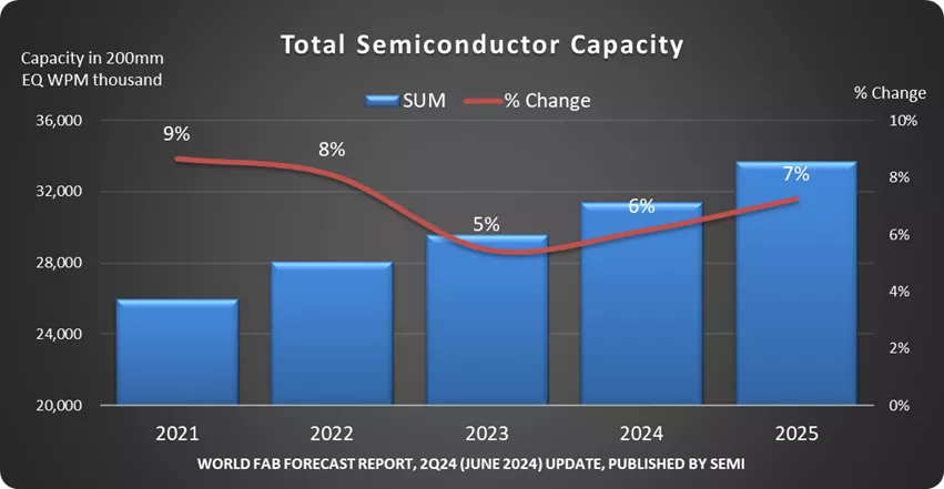


Capacity Expansion by Region

Chinese chipmakers are expected to maintain double-digit capacity growth, registering a 14% increase to 10.1 million wpm in 2025 – nearly a third of the industry’s total – after logging a 15% rise to 8.85 million wpm in 2024. Despite the potential risks of an overshoot, the region continues aggressive investment in its capacity expansion, in part to mitigate the impact of recent export controls. Major foundry suppliers including Huahong Group, Nexchip, Sien Integrated and SMIC and DRAM maker CXMT are investing heavily to grow the region’s semiconductor manufacturing capacity.

Most of the other major chipmaking regions are expected to see capacity growth of no more than 5% in 2025. Taiwan is forecast to rank second in capacity in 2025 at 5.8 million wpm, a 4% growth rate, while South Korea is projected to take the third spot next year, expanding capacity 7% to 5.4 million wpm after surpassing the 5 million wpm mark for the first time in 2024. Japan, the Americas, Europe & Mideast, and Southeast Asia are expected to grow semiconductor manufacturing capacity 4.7 million wpm (3% YoY), 3.2 million wpm (5% YoY), 2.7 million wpm (4% YoY), and 1.8 million wpm (4% YoY), respectively.

Capacity Expansion by Segment

Fueled largely by Intel’s establishment of its foundry business and China’s capacity expansion, the foundry segment is projected to increase capacity 11% in 2024 and 10% in 2025, reaching 12.7 million wpm by 2026.

Rapid adoption of high bandwidth memory (HBM) to meet rising demand for faster processors required by AI servers is powering unprecedented capacity growth in the memory sector. Exploding AI adoption has driven increasing demand for denser HBM stacks, with each stack now integrating 8 to 12 dice. In response, leading DRAM makers are increasing investment in HBM/DRAM. DRAM capacity is expected to increase by 9% in both 2024 and 2025. By contrast, the 3D NAND market recovery remains slow, with no growth in capacity forecast for 2024 and a 5% increase expected in 2025.

The rise of AI applications in edge devices is expected to increase DRAM content in mainstream smartphones from 8GB to 12GB, while laptops using AI assistants will need at least 16GB of DRAM. The expansion of AI to edge devices will also stoke demand for DRAM.

Download a sample of the SEMI World Fab Forecast report.

For details about SEMI reports on other semiconductor sectors, visit SEMI Market Data or contact the SEMI Market Intelligence Team (MIT) at [email protected].

About SEMI
SEMI® is the global industry association connecting over 3,000 member companies and 1.5 million professionals worldwide across the semiconductor and electronics design and manufacturing supply chain. We accelerate member collaboration on solutions to top industry challenges through Advocacy, Workforce Development, Sustainability, Supply Chain Management and other programs. Our SEMICON® expositions and events, technology communities, standards and market intelligence help advance our members’ business growth and innovations in design, devices, equipment, materials, services and software, enabling smarter, faster, more secure electronics. Visit www.semi.org, contact a regional office, and connect with SEMI on LinkedIn and X to learn more.

Association Contacts

Michael Hall/SEMI
Phone: 1.408.943.7988
Email: [email protected]

Christian G. Dieseldorff/SEMI US
Phone: 1.408.943.7940
Email: [email protected]

Chih-Wen Liu/SEMI Taiwan
Phone: 886.3.560.1777
Email: [email protected]

MILPITAS, Calif. — March 19, 2024 — Global 300mm fab equipment spending for front-end facilities is forecast to reach a record US$137 billion in 2027 after topping US$100 billion for the first time by 2025 on the strength of the memory market recovery and strong demand for high-performance computing and automotive applications, SEMI highlighted today in its quarterly 300mm Fab Outlook Report to 2027 report.

Worldwide 300mm fab equipment investment is expected to increase 20% to US$116.5 billion in 2025 and 12% to US$130.5 billion in 2026 before hitting a record high in 2027.
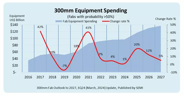

“Projections for the steepening ramp of 300mm fab equipment spending in the coming years reflects the production capacity needed to meet growing demand for electronics across a diverse range of markets as well as a new wave of applications spawned by artificial intelligence (AI) innovation,” said Ajit Manocha, SEMI President and CEO. “The newest SEMI report also highlights the critical importance of increases in government investments in semiconductor manufacturing to bolster economies and security worldwide. This trend is expected to help significantly narrow the equipment spending gap between re-emerging and emerging regions and the historical top-spending regions in Asia.”


Regional Growth

The SEMI 300mm Fab Outlook to 2027 report shows China continuing to lead fab equipment spending with US$30 billion in investments in each of the next four years fueled by government incentives and domestic self-sufficiency policies.

Supported by leading-edge nodes expansion for high-performance computing (HPC) and the memory market recovery, Taiwanese and Korean chip suppliers are increasing their equipment investments. Taiwan is expected to rank second in equipment spending at US$28 billion in 2027, up from US$20.3 billion in 2024, while Korea is expected to rank third at US$26.3 billion in 2027, an increase from US$19.5 billion this year.

The Americas is projected to double 300mm fab equipment investments from US$12 billion in 2024 to US$24.7 billion in 2027, while spending in Japan, Europe & the Middle East, and Southeast Asia are expected to reach US$11.4 billion, US$11.2 billion, and US$5.3 billion in 2027, respectively.

Segment Growth

Foundry segment spending is expected to decline 4% to US$56.6 billion this year due in part to the expected slowdown in mature nodes (>10nm) investment, though the segment continues to log the highest growth among all segments to meet market demand for generative AI, automotive and intelligent edge devices. The segment’s equipment spending is forecast to post a 7.6% compound annual growth rate (CAGR) to US$79.1 billion from 2023 to 2027.

Demand for greater data throughput, crucial for AI servers, is driving strong demand for high-bandwidth memory (HBM) and spurring increased investment in memory technology. Among all segments, memory is ranked second and is expected to post US$41.5 billion in equipment investments in 2027, a 20% CAGR from 2023. DRAM equipment spending is expected to rise to US$25.2 billion in 2027, a 17.4% CAGR, while 3D NAND investment is projected to reach US$16.8 billion in 2027, a 29% CAGR.

The Analog, Micro, Opto, and Discrete segments are projected to increase 300mm fab equipment investments to US$5.5 billion, US$4.3 billion, US$2.3 billion, and US$1.6 billion in 2027, respectively.

The SEMI 300mm Fab Outlook Report to 2027 report lists 405 facilities and lines globally, including 75 high-probability facilities expected to start operation during the four years beginning in 2024. The report reflects 358 updates and 26 new fabs/lines project since its last publication in December 2023.

For more information on the report or to subscribe to SEMI market data, visit SEMI Market Data or contact the SEMI Market Intelligence Team (MIT) at [email protected].

About SEMI

SEMI® is the global industry association connecting over 3,000 member companies and 1.5 million professionals worldwide across the semiconductor and electronics design and manufacturing supply chain. We accelerate member collaboration on solutions to top industry challenges through Advocacy, Workforce Development, Sustainability, Supply Chain Management and other programs. Our SEMICON® expositions and events, technology communities, standards and market intelligence help advance our members’ business growth and innovations in design, devices, equipment, materials, services and software, enabling smarter, faster, more secure electronics. Visit www.semi.org, contact a regional office, and connect with SEMI on LinkedIn and X to learn more.

Association Contacts

Michael Hall/SEMI
Phone: 1.408.943.7988
Email: [email protected]

Christian G. Dieseldorff/SEMI US
Phone: 1.408.943.7940
Email: [email protected]

Chih-Wen Liu/SEMI Taiwan
Phone: 886.3.560.1777
Email: [email protected]

MILPITAS, Calif. — January 2, 2024 — Global semiconductor capacity is expected to increase 6.4% in 2024 to top the 30 million *wafers per month (wpm) mark for the first time after rising 5.5% to 29.6 wpm in 2023, SEMI announced today in its latest quarterly World Fab Forecast report.

The 2024 growth will be driven by capacity increases in leading-edge logic and foundry, applications including generative AI and high-performance computing (HPC), and the recovery in end-demand for chips. The capacity expansion slowed in 2023 due to softening semiconductor market demand and the resulting inventory correction.

“Resurgent market demand and increased government incentives worldwide are powering an upsurge in fab investments in key chipmaking regions and the projected 6.4% rise in global capacity for 2024,” said Ajit Manocha, SEMI President and CEO. “The heightened global attention on the strategic importance of semiconductor manufacturing to national and economic security is a key catalyst of these trends.”

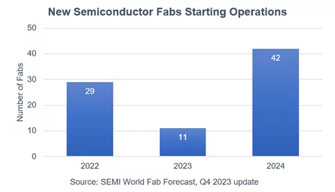
Covering 2022 to 2024, the World Fab Forecast report shows that the global semiconductor industry plans to begin operation of 82 new volume fabs, including 11 projects in 2023 and 42 projects in 2024 spanning wafer sizes ranging from 300mm to 100mm.


China Leads Semiconductor Industry Expansion

Boosted by government funding and other incentives, China is expected to increase its share of global semiconductor production. Chinese chip manufacturers are forecast to start operations of 18 projects in 2024, with 12% YoY capacity growth to 7.6 million wpm in 2023 and 13% YoY capacity growth to 8.6 million wpm in 2024.

Taiwan is projected to remain the second-largest region in semiconductor capacity, increasing capacity 5.6% to 5.4 million wpm in 2023 and posting 4.2% growth to 5.7 million wpm in 2024. The region is poised to begin operations of five fabs in 2024.

Korea ranks third in chip capacity at 4.9 million wpm in 2023 and 5.1 million wpm in 2024, a 5.4% increase as one fab comes online. Japan is expected to place fourth at 4.6 million wpm in 2023 and 4.7 million wpm in 2024, a capacity increase of 2% as it starts operations of four fabs in 2024.

The World Fab Forecast shows the Americas increasing chip capacity by 6% YoY to 3.1 million wpm with six new fabs in 2024. Europe & Mideast is projected to up capacity 3.6% to 2.7 million wpm in 2024 as it launches operations of four new fabs. Southeast Asia is poised to increase capacity 4% to 1.7 million wpm in 2024 with the start of four new fab projects.

Foundry Segment Continues Strong Capacity Growth

Foundry suppliers are forecast to rank as the top semiconductor equipment buyers, increasing capacity to 9.3 million wpm in 2023 and a record 10.2 million wpm in 2024.

The memory segment slowed expansion of capacity in 2023 due to weak demand in consumer electronics including PCs and smartphones. The DRAM segment is expected to increase capacity 2% to 3.8 million wpm in 2023 and 5% to 4 million wpm in 2024. Installed capacity for 3D NAND is projected to remain flat at 3.6 million in 2023 and rise 2% to 3.7 million wpm next year.

In the discrete and analog segments, vehicle electrification remains the key driver of capacity expansion. Discrete capacity is forecast to grow 10% to 4.1 million wpm in 2023 and 7% to 4.4 million wpm in 2024, while Analog capacity is projected to grow 11% to 2.1 million wpm in 2023 and 10% to 2.4 million wpm in 2024.

The latest update of the SEMI World Fab Forecast report, published in December, lists 1,500 facilities and lines globally, including 177 volume facilities and lines with various probabilities expected to start operation in 2023 or later. 

Download a sample of the SEMI World Fab Forecast report.

For details about SEMI reports on other semiconductor sectors, visit SEMI Market Data or contact the SEMI Market Intelligence Team (MIT) at [email protected].

*200mm equivalent

About SEMI
SEMI® connects 3,000 member companies and 1.3 million professionals worldwide to advance the technology and business of electronics design and manufacturing. SEMI members are responsible for the innovations in materials, design, equipment, software, devices, and services that enable smarter, faster, more powerful, and more affordable electronic products. Electronic System Design Alliance (ESD Alliance), FlexTech, the Fab Owners Alliance (FOA), the MEMS & Sensors Industry Group (MSIG), Nano-Bio Materials Consortium (NBMC), and SOI Consortium are SEMI Strategic Technology Communities. Visit www.semi.org, contact one of our worldwide offices, and connect with SEMI on LinkedIn and X (formerly Twitter) to learn more.

Association Contacts

Michael Hall/SEMI US
Phone: 1.408.943.7988
Email: [email protected]

Christian G. Dieseldorff/SEMI US
Phone: 1.408.943.7940
Email: [email protected]

Chih-Wen Liu/SEMI Taiwan
Phone: 886.3.560.1777
Email: [email protected]

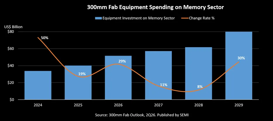
MILPITAS, Calif. – June 29, 2026 – Worldwide 300mm fab equipment investment in the memory sector is projected to surpass $50 billion for the first time in 2026, rising 29% to $52 billion before increasing another 11% to $57 billion in 2027, SEMI reported today in its latest 300mm Fab Outlook. The growth reflects continued AI-driven demand for advanced memory, supported by rising investment in AI infrastructure, data centers, and next-generation computing systems.

Looking further out, global 300mm fab equipment spending in the memory sector is expected to grow at a 19% CAGR from 2024 to 2029. Worldwide 300mm memory capacity is also projected to increase, reaching 4.1 million wafers per month in 2026 and 4.2 million wafers per month in 2027.

“Strong demand for high bandwidth memory and other advanced memory technologies is reshaping investment priorities across the semiconductor supply chain,” said Ajit Manocha, SEMI President and CEO. “As AI infrastructure expands, memory manufacturers are accelerating investments in both capacity and technology migration to support the next wave of data-intensive applications.”

Memory Segment Growth

The 2Q26 edition of the SEMI 300mm Fab Outlook includes an increased projection in 300mm fab equipment spending in the memory sector driven by continued upward capital expenditure plans among leading cloud service providers and strong demand for AI accelerators. DRAM equipment spending is expected to grow 29% to $37 billion in 2026, supported by strong HBM and DDR5 demand for GPUs and other AI accelerators. Equipment spending on 3D NAND is also projected to rise 28% to $14 billion in 2026, supported by increasing data storage requirements tied to AI deployment.

Continued investment in advanced-node DRAM and higher-layer 3D NAND is supporting a stronger memory capacity outlook, which has been revised upward in the 2Q26 edition of the SEMI 300mm Fab Outlook. Effective capacity growth, however, remains moderated by technology migration and process complexity, including advanced-node DRAM, HBM, and higher-layer NAND transitions.

The SEMI 300mm Fab Outlook lists 413 facilities and lines globally. The report reflects 155 updates and addition of 7 new fabs/lines projects since its last publication in March 2026. 

For more information on the report or to subscribe, please contact the SEMI Market Intelligence Team at [email protected]. More details are also available on the SEMI Market Data webpage.  

Follow SEMI Market Intelligence

Follow SEMI 

About SEMI

SEMI® is the global industry association connecting over 4,000 companies and 1.5 million professionals worldwide across the semiconductor and electronics design and manufacturing supply chain. We accelerate member collaboration on solutions to top industry challenges through Advocacy, Workforce Development, Sustainability, Supply Chain Management and other programs. Our SEMICON® expositions and events, technology communities, standards and market intelligence help advance our members’ business growth and innovations in design, devices, equipment, materials, services and software, enabling smarter, faster, more secure electronics. Visit www.semi.org, contact a regional office, and connect with SEMI on LinkedIn and X to learn more.  


RENA Technologies GmbH, a long-standing and experienced manufacturer of wet processing solutions for the semiconductor, advanced packaging, and solar industries, has been awarded a multi-million Euro order by a leading European semiconductor manufacturer for a specialized cleaning application designed for advanced substrates.

The solution is based on a high-performance batch wet processing platform and has been specifically engineered to deliver ultra-clean and highly efficient processing of demanding substrates. By combining advanced process control with a scalable batch architecture, the system ensures outstanding process stability, repeatability, and optimized throughput.

The customer’s decision underscores the technological strength and competitiveness of RENA’s wet processing solutions. Particularly when handling complex substrate materials, the application provides significant advantages in quality assurance, process control, and overall production efficiency. The mature cleanroom capabilities, excellent process control, and high- volume automation solutions of RENA add up to the perfect fit for the customer’s needs.

With this order, RENA further strengthens its position in the European semiconductor market and reinforces its commitment to delivering innovative, locally supported solutions to key industry players.

“Our success in securing this project highlights the growing demand for advanced wet processing technologies in Europe,” said Peter Schneidewind, CEO of RENA Technologies GmbH. “With more than 80 glass treatment tools in production worldwide - including cutting etch TGV/advanced packaging applications - RENA´s sophisticated technological solutions prove again in this new application for specialized semiconductor substrates.”

Date: May 8, 2026

Location: Drammen, Norway

Board-level and semiconductor test data are often analyzed separately, limiting correlation across the product lifecycle. Linking PCB assembly (PCBA) test results, including in-circuit and functional test, with upstream wafer, sort, and final test data remains difficult, particularly in photonics, advanced packaging, and high-density integration environments. yieldWerx and WATS announce a partnership to bridge this gap in the PCB test and semiconductor manufacturing workflows.

WATS is a test data management platform purpose-built for electronics manufacturers. It captures, standardizes, and analyzes high-volume test data from PCBA (printed circuit board assembly) production environments, including in-circuit test (ICT), functional test, and final test, giving engineers real-time visibility into board-level yield, anomalies, and quality metrics across the production line.

yieldWerx operates at the semiconductor level, connecting data across wafer fabrication, wafer sort, die, and packaged device test. Its enterprise analytics platform enables advanced yield analysis, traceability, and root cause investigation from design through silicon manufacturing.

Together, the platforms address the full product stack. This allows manufacturers to correlate PCBA-level signals with silicon quality data, improving visibility across test stages and enabling more effective analysis of yield and reliability issues.

Customer and industry benefits include:

Real-time PCBA test visibility for faster identification of yield and quality issues

Improved correlation between board-level test results and upstream chip or wafer data

Reduced time spent reconciling data across disconnected systems

Earlier detection of cross-stage patterns impacting yield and reliability

Faster root cause analysis spanning silicon, assembly, and board-level test

Better alignment between electronics manufacturing and semiconductor supply chain

The combined solution supports open architectures, APIs, and flexible deployment models, enabling integration without large-scale system changes.

About yieldWerx

yieldWerx is an enterprise analytics platform connecting data across the semiconductor product lifecycle, from design and wafer fabrication through wafer sort, die, and packaged device test, enabling advanced yield analysis, traceability, and data-driven decision-making across cloud, on-premises, and hybrid environments.

About WATS

WATS is a test data management and analytics platform developed by Virinco, built to collect, standardize, and analyze data from electronics manufacturing test systems. It provides real-time visibility into board-level performance across ICT, functional test, and final test operations, helping engineers monitor yield, detect anomalies, and improve quality at high volume.

Statements from Leadership
"We are excited to partner with yieldWerx. Our customers manufacture complex electronics where board-level test data alone only tells part of the story. By connecting PCBA production test data with yieldWerx's upstream semiconductor intelligence, we can give them a more complete picture of their product quality and yield." -- Tom Lomsdalen, CEO, Wats

“Our customers have been asking for a unified view that links semiconductor yield data with downstream electronics test results, and this partnership delivers exactly that. Together, yieldWerx and WATS empower engineering teams to move faster on root cause analysis, reduce escapes, and make smarter decisions across the entire product lifecycle.” -- Aftkhar Aslam, CEO, yieldWerx

For further information, please visit https://www.yieldWerx.com or https://www.Wats.com/.

Semiconductor industry leader takes the helm to accelerate Beneq’s next phase of growth in atomic layer deposition

Espoo, Finland, 8 May, 2026 – Beneq Oy, the home of atomic layer deposition (ALD), today announced the appointment of Dr. Jason Harrison as Chief Executive Officer. Dr. Harrison succeeds Dr. Tommi Vainio and will lead Beneq into its next phase of growth across semiconductor, optical, and emerging technology markets.

A Strategic Leadership Transition
Beneq enters its next phase of growth from a position of strong commercial momentum. Recent milestones include the qualification of the Beneq Transform® cluster tool for volume production of GaN power and RF filter devices; the introduction of Beneq Transmute™ and Beneq Transform® XP, both engineered for high-volume manufacturing (HVM) of specialty semiconductors; growing adoption of the P-Series for coating critical chamber parts in advanced node devices; and selection of the C2R™ for AR waveguide production in next-generation XR optics.

Against this backdrop, the Board of Directors has determined that the time is right to align executive leadership with the company's evolving strategic priorities. As part of this transition, Dr. Tommi Vainio has decided to step down as CEO to pursue other opportunities. The Board of Directors extends its sincere thanks to Tommi, whose leadership advanced Beneq's technology platform, strengthened its market position in thin film deposition, and guided the company through important stages of its development.

A Proven Leader for a Scaling ALD Business
Dr. Harrison brings extensive global experience across the semiconductor and advanced technology sectors. He holds a Ph.D. in Quantum Chemistry and has built a distinguished career spanning device manufacturing, process development, and equipment solutions, with senior leadership roles at Intel, Lam Research, Veeco, and Applied Materials covering research and development, new product introduction, global account management, and business unit leadership. This combination of technical depth and commercial acumen positions him to scale Beneq’s commercial execution and growth across its global customer base.

Looking Ahead
Under Jason’s leadership, Beneq will accelerate strategic execution across its expanding portfolio, deepen customer engagement across North America, Asia, and Europe, and continue investing in innovative ALD solutions from R&D to HVM to deliver long-term value to customers, employees, and stakeholders.

Dr. Patrick Rabinzohn, Member of the Board of Directors, Beneq, said: “Jason brings the technical depth, the business and account management experience, and the global perspective Beneq needs at this stage of its growth. His academic background and compelling track record across the semiconductor industry positions Jason to build on the momentum the company generated especially.”

Dr. Jason Harrison, Chief Executive Officer, Beneq, added: “Beneq has a strong technology foundation, a talented team, and a growing pipeline of customers in some of the most important markets in semiconductors and optics. I look forward to working with the team to accelerate execution and deliver on the trust our customers place in us.”

About Beneq
Beneq pioneered industrial production of Atomic Layer Deposition (ALD) with the introduction of the first commercial ALD equipment in 1984. Today, Beneq advances ALD adoption and validation with a portfolio that includes the Beneq Transform®, Transform XP, Transform 300, and Transmute™ for specialty semiconductor device fabrication; TFS 200 and TFS 500 for R&D; the P400A, P800, and P1500 batch systems for coating critical semiconductor chamber components and complex part geometries; and spatial ALD platforms such as the C2R™ and roll-to-roll processing equipment. Headquartered in Espoo, Finland, Beneq enables ALD integration from lab to fab for semiconductors, optics, and functional coatings.

Press Contacts
Lie Luo
Head of Marketing
[email protected]

ROSENHEIM, Germany / KUALA LUMPUR, 5 May 2026 — esmo group (esmo), a leading global full-service systems integrator, developer, and supplier of advanced automation solutions for the semiconductor test industry, today announces the debut of its X-change Cart. A dedicated, semi-automated Device Interface Board (DIB) exchange system that enables a complete load board changeover by a single operator in under one minute, the X-change Cart addresses the safety, efficiency, and reliability challenges associated with manual board handling on the semiconductor test floor.

In high-mix semiconductor test environments, load board changeovers are a frequent and operationally significant activity. The reliance on manual handling has long presented challenges around changeover time, operator safety, and the risk of damage to high-value boards.

“Across test floors, we kept seeing the same pattern,” said Josef Weinberger, Head of Business Unit, esmo semicon. “Board changeovers were slow, physically demanding, and too dependent on individual technique. In tight spaces, that's where mistakes happen and time is lost. That observation drove us to build a dedicated solution that makes changeovers fast, repeatable, and manageable by a single operator in under a minute.”

Engineered for the Modern Test Floor

The X-change Cart removes the physical demands and variability of manual board handling from the equation entirely. Through a structured, HMI-controlled process, a single operator can lock, rotate, and transfer a board to the tester within a minute. The ability to carry two boards in a single trip makes that timescale achievable in practice. Thoughtful design details, including a ±180° rotation at the locking mechanism and a ±90° tower swivel, address the real-world constraints of a busy test floor.

Broad compatibility with leading ATE platforms (e.g. Teradyne, Advantest, SPEA and more) facilitates integration into existing multi-vendor environments without reconfiguration, allowing OSATs and IDMs to realise multiple benefits without disruption to their current setup.

For facilities with longer-term automation objectives, an optional configuration allows the interface tower to be mounted onto a customized AGV or AMR, providing a practical upgrade path toward autonomous test floor operations. The modular design further allows additional features to be incorporated as operational requirements evolve.

Weinberger added, “Reliability in production comes down to the details. The gripper head is engineered to perform consistently under real production conditions, with ESD-safe construction ensuring the board is protected at every point of contact. That level of engineering discipline is what makes the difference on a real production floor.”

X-change Cart Key Features

  • Modular DIB exchange system for reliable, error-free board loading and unloading
  • One-person operation — complete board change in under one minute
  • Transports two load boards simultaneously for rapid exchange
  • Full multi-axis rotation: ±180° at locking mechanism | ±180° Y-axis | ±90° Z-axis
  • Compatible with leading ATE platforms — Teradyne, Advantest, SPEA and more
  • Interfaces with test head, prober, DIB-loader, storage rack, and maintenance workbench
  • Tower swivels ±90° for use in narrow corridors and constrained test floor layouts
  • Integrated Human-Machine Interface (HMI), sensor detection, safety hand-brake, and modular battery
  • Optional: fully automated configuration mountable on AGV or AMR

The X-change Cart will be available for live demonstration at the esmo booth throughout SEMICON Southeast Asia 2026. Visit esmo at Booth 2145, Hall 8, Level 2, MITEC Kuala Lumpur from 5–7 May 2026, or contact [email protected] to arrange a meeting or request further information.

Kuala Lumpur, Malaysia, 29 April 2026 – DAS Environmental Experts presents its latest sustainable technologies at SEMICON SEA 2026 (May 5–7, MITEC, Booth 1174). The focus is on closing resource loops in semiconductor manufacturing through integrated waste gas and water treatment.

Integrated environmental technologies for next-generation fabs

DAS Environmental Experts demonstrates how point-of-use waste gas treatment can be seamlessly combined with advanced water recycling to create an integrated solution. This approach reduces both resource consumption and emissions, actively supporting closed-loop concepts for water and materials.

By strategically linking waste gas and wastewater management, the company enables measurable efficiency and sustainability gains directly at the source. DAS Environmental Experts provides a comprehensive range of point-of-use (POU) and end-of-pipe solutions, all tailored to specific customer requirements. This holistic strategy reflects the growing industry imperative for integrated waste and water management in modern semiconductor fabs.

Reliable waste gas treatment: LARCH PLUS DUO

The LARCH PLUS DUO is engineered for maximum operational reliability. This burn-dry system is specifically designed to treat waste gases from MOCVD processes for LEDs, μLEDs and GaN, as well as from EUV processes, directly at the point of use.

It combines two fully independent units running in parallel. Intelligent piping and internal data exchange provide full redundancy and ensure continuous operation, even during maintenance or in the event of a malfunction on one side.

The system operates without fresh water, generates no wastewater, and minimizes environmental impact with zero CO₂ emissions and low NOx emissions.

Resource Recovery & Water Recycling

The company also highlights solutions for material recovery and water reuse. By treating wastewater from grinding and abatement processes, valuable materials like gallium, germanium, and copper are recovered. The modular design allows easy integration into existing fabs and supports retrofit applications, helping operators improve environmental performance while reducing dependency on primary raw materials.

Expert presentation

As part of the conference program, Falk Allmrodt (Key Account Manager) will present "Raising CF₄ Abatement Efficiency Standards in Semiconductor Manufacturing: Beyond Industry Benchmarks" on Thursday, May 7, at 14:55 hrs (Novel 1, Level 1A).

The team welcomes visitors at Booth 1174 to discuss innovative paths to sustainable manufacturing.

About DAS Environmental Experts
DAS Environmental Experts (DAS EE) is a leading international provider of comprehensive environmental technology solutions in the fields of waste gas and water treatment. Founded in Dresden, Germany, in 1991, the company supports industrial enterprises worldwide in safely treating emissions, using resources efficiently and reliably complying with environmental standards.

With 950+ employees and locations in nine countries, the DAS Group combines global expertise with local presence. These solutions, developed and manufactured in Germany, stand for the highest quality and technological innovation.

As one of the top three companies in waste gas treatment, DAS EE offers the semiconductor industry unique, integrated solutions combining waste gas and wastewater treatment.

The company’s portfolio encompasses plants, system solutions and services across the entire process chain—from planning and implementation through to operation. Enhanced by digital solutions, the technologies ensure maximum efficiency and reliable operations.

Its customers include companies from the semiconductor, LED, solar, chemical, pharmaceutical, cosmetics and food industries. The range of services is complemented by Innovation and Support Centers (ISC) in Dresden, Taiwan and the USA.

Governor Abbott joined leadership from The Texas A&M University System and Texas Representative Paul Dyson on April 9 to break ground for the nearly 80,000-square-foot facility for the Texas A&M Semiconductor Institute (TSI).

"Texas and America must be microchip independent," said Governor Abbott. "We must ensure we lead the way forward. This groundbreaking is a giant step toward achieving that independence. Texas A&M is accelerating in innovation, and cementing Texas' position as the global leader for semiconductors."

The A&M System Board of Regents approved the establishment of TSI in May 2023 in response to federal and state-level CHIPS and Science Act legislation. By June 2023, Gov. Abbott signed the Texas CHIPS Act that appropriated $1.4 billion for semiconductor research, development and manufacturing in Texas, with $226.4 million directly allocated to the A&M System.

“At the A&M System, our job is to see where the state and country are going — and build ahead of it,” said Jay Graham, vice chairman of the Board of Regents. “This project does exactly that. It strengthens Texas. It strengthens our workforce. And it strengthens the country.”

“This is a facility designed for semiconductor research and workforce training,” said Glenn Hegar, chancellor for the A&M System. “It includes advanced cleanrooms, fabrication space and flexible labs to mirror real-world production environments. That is how you build a workforce and strengthen an industry.”

The A&M System named Dr. E. Steve Putna the inaugural director of TSI in July 2024. Putna came to TSI with more than 25 years of extensive experience in the semiconductor industry, particularly in manufacturing and supply chain management at Intel Corporation.

“This groundbreaking marks a significant step forward for TSI,” said Putna. “We are celebrating more than a new building; we are celebrating our collective mission to drive economic growth in Texas through workforce development; disruptive, next-generation research; and impactful collaborations in support of national security and the semiconductor resurgence in the United States.”