
downloadGroupGroupnoun_press release_995423_000000 copyGroupnoun_Feed_96767_000000Group 19noun_pictures_1817522_000000Member company iconResource item iconStore item iconGroup 19Group 19noun_Photo_2085192_000000 Copynoun_presentation_2096081_000000Group 19Group Copy 7noun_webinar_692730_000000Path
Skip to main content
Default Banner Image

Fab

MILPITAS, Calif. – June 18, 2024 – To keep pace with unremitting growth in demand for chips, the global semiconductor manufacturing industry is expected to increase capacity by 6% in 2024 and post a 7% gain in 2025, reaching a record capacity high of 33.7 million wafers per month (wpm: 8-inch equivalent), SEMI announced today in its latest quarterly World Fab Forecast report.

Leading-edge capacity for 5nm nodes and under is expected to grow 13% in 2024, chiefly driven by generative artificial intelligence (AI) for data center training, inference, and leading-edge devices. To increase processing power efficiency, chipmakers including Intel, Samsung, and TSMC are poised to start production of 2nm Gate-All-Around (GAA) chips, boosting total leading-edge capacity growth by 17% in 2025.

“The proliferation of AI processing, from cloud computing to edge devices, is fueling the race to develop high-performance chips and driving a robust expansion of global semiconductor manufacturing capacity,” said Ajit Manocha, SEMI President and CEO. “This creates a virtuous cycle: AI will drive the growth of semiconductor content across a diverse range of applications, which in turn encourages further investment.”
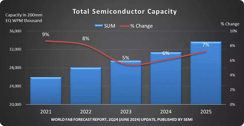


Capacity Expansion by Region

Chinese chipmakers are expected to maintain double-digit capacity growth, registering a 14% increase to 10.1 million wpm in 2025 – nearly a third of the industry’s total – after logging a 15% rise to 8.85 million wpm in 2024. Despite the potential risks of an overshoot, the region continues aggressive investment in its capacity expansion, in part to mitigate the impact of recent export controls. Major foundry suppliers including Huahong Group, Nexchip, Sien Integrated and SMIC and DRAM maker CXMT are investing heavily to grow the region’s semiconductor manufacturing capacity.

Most of the other major chipmaking regions are expected to see capacity growth of no more than 5% in 2025. Taiwan is forecast to rank second in capacity in 2025 at 5.8 million wpm, a 4% growth rate, while South Korea is projected to take the third spot next year, expanding capacity 7% to 5.4 million wpm after surpassing the 5 million wpm mark for the first time in 2024. Japan, the Americas, Europe & Mideast, and Southeast Asia are expected to grow semiconductor manufacturing capacity 4.7 million wpm (3% YoY), 3.2 million wpm (5% YoY), 2.7 million wpm (4% YoY), and 1.8 million wpm (4% YoY), respectively.

Capacity Expansion by Segment

Fueled largely by Intel’s establishment of its foundry business and China’s capacity expansion, the foundry segment is projected to increase capacity 11% in 2024 and 10% in 2025, reaching 12.7 million wpm by 2026.

Rapid adoption of high bandwidth memory (HBM) to meet rising demand for faster processors required by AI servers is powering unprecedented capacity growth in the memory sector. Exploding AI adoption has driven increasing demand for denser HBM stacks, with each stack now integrating 8 to 12 dice. In response, leading DRAM makers are increasing investment in HBM/DRAM. DRAM capacity is expected to increase by 9% in both 2024 and 2025. By contrast, the 3D NAND market recovery remains slow, with no growth in capacity forecast for 2024 and a 5% increase expected in 2025.

The rise of AI applications in edge devices is expected to increase DRAM content in mainstream smartphones from 8GB to 12GB, while laptops using AI assistants will need at least 16GB of DRAM. The expansion of AI to edge devices will also stoke demand for DRAM.

Download a sample of the SEMI World Fab Forecast report.

For details about SEMI reports on other semiconductor sectors, visit SEMI Market Data or contact the SEMI Market Intelligence Team (MIT) at [email protected].

About SEMI
SEMI® is the global industry association connecting over 3,000 member companies and 1.5 million professionals worldwide across the semiconductor and electronics design and manufacturing supply chain. We accelerate member collaboration on solutions to top industry challenges through Advocacy, Workforce Development, Sustainability, Supply Chain Management and other programs. Our SEMICON® expositions and events, technology communities, standards and market intelligence help advance our members’ business growth and innovations in design, devices, equipment, materials, services and software, enabling smarter, faster, more secure electronics. Visit www.semi.org, contact a regional office, and connect with SEMI on LinkedIn and X to learn more.

Association Contacts

Michael Hall/SEMI
Phone: 1.408.943.7988
Email: [email protected]

Christian G. Dieseldorff/SEMI US
Phone: 1.408.943.7940
Email: [email protected]

Chih-Wen Liu/SEMI Taiwan
Phone: 886.3.560.1777
Email: [email protected]

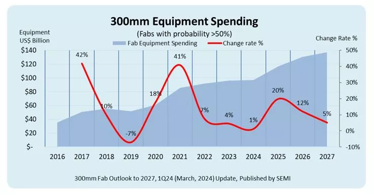
MILPITAS, Calif. — March 19, 2024 — Global 300mm fab equipment spending for front-end facilities is forecast to reach a record US$137 billion in 2027 after topping US$100 billion for the first time by 2025 on the strength of the memory market recovery and strong demand for high-performance computing and automotive applications, SEMI highlighted today in its quarterly 300mm Fab Outlook Report to 2027 report.

Worldwide 300mm fab equipment investment is expected to increase 20% to US$116.5 billion in 2025 and 12% to US$130.5 billion in 2026 before hitting a record high in 2027.

“Projections for the steepening ramp of 300mm fab equipment spending in the coming years reflects the production capacity needed to meet growing demand for electronics across a diverse range of markets as well as a new wave of applications spawned by artificial intelligence (AI) innovation,” said Ajit Manocha, SEMI President and CEO. “The newest SEMI report also highlights the critical importance of increases in government investments in semiconductor manufacturing to bolster economies and security worldwide. This trend is expected to help significantly narrow the equipment spending gap between re-emerging and emerging regions and the historical top-spending regions in Asia.”


Regional Growth

The SEMI 300mm Fab Outlook to 2027 report shows China continuing to lead fab equipment spending with US$30 billion in investments in each of the next four years fueled by government incentives and domestic self-sufficiency policies.

Supported by leading-edge nodes expansion for high-performance computing (HPC) and the memory market recovery, Taiwanese and Korean chip suppliers are increasing their equipment investments. Taiwan is expected to rank second in equipment spending at US$28 billion in 2027, up from US$20.3 billion in 2024, while Korea is expected to rank third at US$26.3 billion in 2027, an increase from US$19.5 billion this year.

The Americas is projected to double 300mm fab equipment investments from US$12 billion in 2024 to US$24.7 billion in 2027, while spending in Japan, Europe & the Middle East, and Southeast Asia are expected to reach US$11.4 billion, US$11.2 billion, and US$5.3 billion in 2027, respectively.

Segment Growth

Foundry segment spending is expected to decline 4% to US$56.6 billion this year due in part to the expected slowdown in mature nodes (>10nm) investment, though the segment continues to log the highest growth among all segments to meet market demand for generative AI, automotive and intelligent edge devices. The segment’s equipment spending is forecast to post a 7.6% compound annual growth rate (CAGR) to US$79.1 billion from 2023 to 2027.

Demand for greater data throughput, crucial for AI servers, is driving strong demand for high-bandwidth memory (HBM) and spurring increased investment in memory technology. Among all segments, memory is ranked second and is expected to post US$41.5 billion in equipment investments in 2027, a 20% CAGR from 2023. DRAM equipment spending is expected to rise to US$25.2 billion in 2027, a 17.4% CAGR, while 3D NAND investment is projected to reach US$16.8 billion in 2027, a 29% CAGR.

The Analog, Micro, Opto, and Discrete segments are projected to increase 300mm fab equipment investments to US$5.5 billion, US$4.3 billion, US$2.3 billion, and US$1.6 billion in 2027, respectively.

The SEMI 300mm Fab Outlook Report to 2027 report lists 405 facilities and lines globally, including 75 high-probability facilities expected to start operation during the four years beginning in 2024. The report reflects 358 updates and 26 new fabs/lines project since its last publication in December 2023.

For more information on the report or to subscribe to SEMI market data, visit SEMI Market Data or contact the SEMI Market Intelligence Team (MIT) at [email protected].

About SEMI

SEMI® is the global industry association connecting over 3,000 member companies and 1.5 million professionals worldwide across the semiconductor and electronics design and manufacturing supply chain. We accelerate member collaboration on solutions to top industry challenges through Advocacy, Workforce Development, Sustainability, Supply Chain Management and other programs. Our SEMICON® expositions and events, technology communities, standards and market intelligence help advance our members’ business growth and innovations in design, devices, equipment, materials, services and software, enabling smarter, faster, more secure electronics. Visit www.semi.org, contact a regional office, and connect with SEMI on LinkedIn and X to learn more.

Association Contacts

Michael Hall/SEMI
Phone: 1.408.943.7988
Email: [email protected]

Christian G. Dieseldorff/SEMI US
Phone: 1.408.943.7940
Email: [email protected]

Chih-Wen Liu/SEMI Taiwan
Phone: 886.3.560.1777
Email: [email protected]

MILPITAS, Calif. — January 2, 2024 — Global semiconductor capacity is expected to increase 6.4% in 2024 to top the 30 million *wafers per month (wpm) mark for the first time after rising 5.5% to 29.6 wpm in 2023, SEMI announced today in its latest quarterly World Fab Forecast report.

The 2024 growth will be driven by capacity increases in leading-edge logic and foundry, applications including generative AI and high-performance computing (HPC), and the recovery in end-demand for chips. The capacity expansion slowed in 2023 due to softening semiconductor market demand and the resulting inventory correction.
“Resurgent market demand and increased government incentives worldwide are powering an upsurge in fab investments in key chipmaking regions and the projected 6.4% rise in global capacity for 2024,” said Ajit Manocha, SEMI President and CEO. “The heightened global attention on the strategic importance of semiconductor manufacturing to national and economic security is a key catalyst of these trends.”

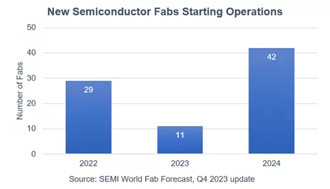
Covering 2022 to 2024, the World Fab Forecast report shows that the global semiconductor industry plans to begin operation of 82 new volume fabs, including 11 projects in 2023 and 42 projects in 2024 spanning wafer sizes ranging from 300mm to 100mm.


China Leads Semiconductor Industry Expansion

Boosted by government funding and other incentives, China is expected to increase its share of global semiconductor production. Chinese chip manufacturers are forecast to start operations of 18 projects in 2024, with 12% YoY capacity growth to 7.6 million wpm in 2023 and 13% YoY capacity growth to 8.6 million wpm in 2024.

Taiwan is projected to remain the second-largest region in semiconductor capacity, increasing capacity 5.6% to 5.4 million wpm in 2023 and posting 4.2% growth to 5.7 million wpm in 2024. The region is poised to begin operations of five fabs in 2024.

Korea ranks third in chip capacity at 4.9 million wpm in 2023 and 5.1 million wpm in 2024, a 5.4% increase as one fab comes online. Japan is expected to place fourth at 4.6 million wpm in 2023 and 4.7 million wpm in 2024, a capacity increase of 2% as it starts operations of four fabs in 2024.

The World Fab Forecast shows the Americas increasing chip capacity by 6% YoY to 3.1 million wpm with six new fabs in 2024. Europe & Mideast is projected to up capacity 3.6% to 2.7 million wpm in 2024 as it launches operations of four new fabs. Southeast Asia is poised to increase capacity 4% to 1.7 million wpm in 2024 with the start of four new fab projects.

Foundry Segment Continues Strong Capacity Growth

Foundry suppliers are forecast to rank as the top semiconductor equipment buyers, increasing capacity to 9.3 million wpm in 2023 and a record 10.2 million wpm in 2024.

The memory segment slowed expansion of capacity in 2023 due to weak demand in consumer electronics including PCs and smartphones. The DRAM segment is expected to increase capacity 2% to 3.8 million wpm in 2023 and 5% to 4 million wpm in 2024. Installed capacity for 3D NAND is projected to remain flat at 3.6 million in 2023 and rise 2% to 3.7 million wpm next year.

In the discrete and analog segments, vehicle electrification remains the key driver of capacity expansion. Discrete capacity is forecast to grow 10% to 4.1 million wpm in 2023 and 7% to 4.4 million wpm in 2024, while Analog capacity is projected to grow 11% to 2.1 million wpm in 2023 and 10% to 2.4 million wpm in 2024.

The latest update of the SEMI World Fab Forecast report, published in December, lists 1,500 facilities and lines globally, including 177 volume facilities and lines with various probabilities expected to start operation in 2023 or later. 

Download a sample of the SEMI World Fab Forecast report.

For details about SEMI reports on other semiconductor sectors, visit SEMI Market Data or contact the SEMI Market Intelligence Team (MIT) at [email protected].

*200mm equivalent

About SEMI
SEMI® connects 3,000 member companies and 1.3 million professionals worldwide to advance the technology and business of electronics design and manufacturing. SEMI members are responsible for the innovations in materials, design, equipment, software, devices, and services that enable smarter, faster, more powerful, and more affordable electronic products. Electronic System Design Alliance (ESD Alliance), FlexTech, the Fab Owners Alliance (FOA), the MEMS & Sensors Industry Group (MSIG), Nano-Bio Materials Consortium (NBMC), and SOI Consortium are SEMI Strategic Technology Communities. Visit www.semi.org, contact one of our worldwide offices, and connect with SEMI on LinkedIn and X (formerly Twitter) to learn more.

Association Contacts

Michael Hall/SEMI US
Phone: 1.408.943.7988
Email: [email protected]

Christian G. Dieseldorff/SEMI US
Phone: 1.408.943.7940
Email: [email protected]

Chih-Wen Liu/SEMI Taiwan
Phone: 886.3.560.1777
Email: [email protected]

Combined software/hardware solution enables chip makers to conduct comprehensive compliance tests of semiconductor manufacturing equipment upon integration in wafer fabs

SEMICON West, San Francisco, USA, October 14, 2026 – Agileo Automation, a leading global provider of control, connectivity, and testing solutions for semiconductor manufacturing, today announces that it has appointed Semitorr – CTW Solutions as distributor of its E84 PIO Box/Speech Scenario combined solution for the North American fab market. The company is a critical parts, materials, equipment, repairs, and value-added services supplier based in Austin, Texas. Agileo’s software/hardware solution enables chip manufacturers to conduct comprehensive compliance tests of semiconductor manufacturing equipment and accelerate their integration in wafer fabs.

The E84 PIO Box is a plug-and-play handheld device that offers a lightweight interface for fab staff to test semiconductor equipment software for compliance with SEMI’s E84 and GEM300 standards suite for automatic carrier delivery upon commissioning in the fabs. It improves the readability, identification, and validation of E84 signal exchanges and functional aspects in cleanrooms or workshops. When integrated with Agileo’s Speech Scenario software that emulates the fab host and validates the SECS/GEM interface with predefined test scenarios, the E84 PIO Box can easily emulate automated carrier delivery systems such as overhead hoist transport or automated guided vehicles. It is able to detect non-compliance and other functional issues thanks to its close alignment with SEMI’s E84 standard.

The solution also supports fab modernization programs in which automated carrier delivery is extended beyond traditional overhead transport systems. By emulating hand-off sequences involving automated guided vehicles (AGVs) and autonomous mobile robots (AMRs), it enables fabs and equipment manufacturers to validate E84 interfaces before deployment, reduce integration risks, and prepare existing or new equipment for flexible automated material handling.

“CTW Solutions stood out for their deep, hands-on experience supporting semiconductor and high-technology industries across North America,” explains Marc Engel, CEO of Agileo Automation. “Their expertise and relationships in this market make them the ideal partner to accelerate Agileo's growth in the region and we are thrilled to welcome them to the Agileo family of distributors.”

“Chip makers face intense pressure to demonstrate E84 compliance quickly and reliably when integrating new semiconductor equipment into their wafer fabs. Agileo's combined E84 PIO Box and Speech Scenario solution is the most complete, field-proven answer to that challenge,” adds Lamont Humphrey, vice president and business unit manager for Semitorr – CTW Solutions. “Representing Agileo in North America is an exciting opportunity and we look forward to bringing this capability to our customers.”

- ends -

About Agileo Automation
Agileo Automation is a trusted partner for equipment manufacturers, helping them build smarter, automated, and more connected machines that integrate seamlessly into advanced semiconductor fabs. Founded in 2010 in Poitiers, France, Agileo helps OEMs with control, communication, data acquisition, and testing across their tools through proven software and expert support. Its flagship A²ECF-SEMI framework provides a solid foundation for developing equipment controllers fully aligned with SEMI SECS/GEM, GEM300, and EDA standards. As an active member of SEMI and the OPC Foundation, Agileo Automation contributes directly to shaping the standards that drive manufacturing. For more information, please visit our website or follow us on LinkedIn.

Gütenbach, Germany, October 2026: RENA Technologies has received three additional major orders for high-throughput equipment for the wet-chemical processing of 200 mm and 300 mm wafers. The systems are destined for semiconductor manufacturers with production sites in Europe, Asia, and the United States.
Key factors in the contract awards included the flexibility to integrate customer-specific options into the equipment concepts. These options enable a higher degree of automation, enhanced process control, and unattended operation. At the same time, they provide the basis for stable process conditions and a long-term reduction in total cost of ownership. High equipment availability, efficient energy consumption, and reduced maintenance requirements all contribute to this. Fewer unplanned downtimes and reproducible processes also help lower operating costs throughout the system’s entire life cycle.

High-Precision Wet Processing for 300 mm Wafers
Two fully automated systems for processing 300 mm wafers focus on wet-chemical etching processes that require particularly high uniformity across the entire wafer surface. Uniform material removal helps ensure that defined process parameters are maintained reproducibly and prepares the wafers for subsequent production steps.
The etching process is followed by high-precision cleaning sequences designed to remove contaminants and particles down to the nanometer scale. Automated wafer handling and continuous monitoring of the relevant process parameters enable stable and reproducible processing without constant operator intervention.

Precision and Automation in 200 mm Wafer Cleaning
Another order comprises a high-throughput cleaning system for 200 mm wafers. This process concept is designed to meet the increasing particle-control requirements of 200 mm wafer manufacturing. Automated process sequences, continuous monitoring of relevant process parameters, and customer-specific functions support consistently high cleaning quality.

“These orders demonstrate the importance of flexible equipment concepts, customer-specific functions, short delivery times, and precise process control for demanding semiconductor processes. With our fully automated systems, we help customers expand their production capacities while achieving stable, reproducible processes and a high degree of automation,” explains Peter Schneidewind, CEO of RENA Technologies. “At the same time, the orders confirm the international confidence in our proven platforms, technology and process expertise.”

About RENA Technologies GmbH
RENA Technologies is a leading global supplier of production machines for wet chemical surface preparation. RENA products are used in path-breaking application fields such as semiconductors, MedTech, renewable energies and the glass industry. RENA equipment is used to treat or modify surfaces of, for example, semiconductor wafers, solar cells, glass, optical substrates, or other high-tech products using wet chemical processes. RENA offers proven standard machines as well as customer-specific solutions and process support.

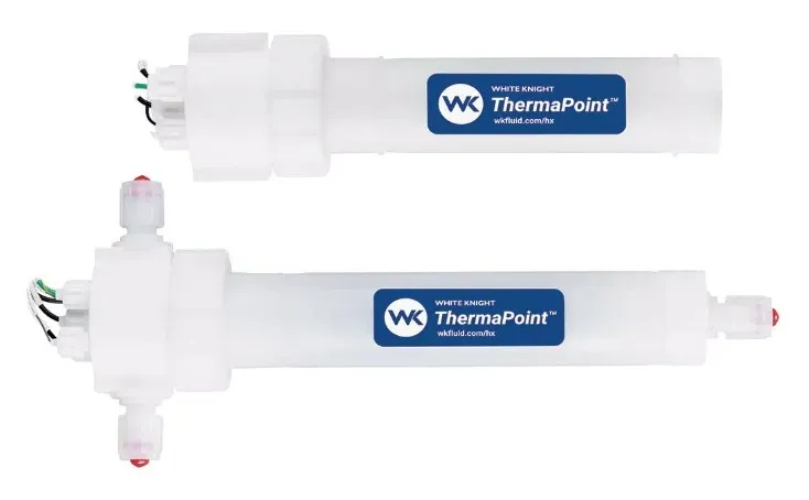
KAMAS, UTAH – White Knight Fluid Handling, a provider of high-purity fluid handling equipment and a Graco company, today announced the launch of its ThermaPoint™ Compact Inline Heaters. Engineered for ultrapure, low-flow, and point-of-use applications within the semiconductor and life sciences industries, ThermaPoint combines a remarkably small footprint with advanced Heateflex® technology designed to deliver rapid, powerful temperature responses. 

ThermaPoint combines robust PFA/PTFE wetted surfaces with a unique tongue-and-groove seal design, eliminating O-ring material compatibility concerns in aggressive-fluid applications. Its Operating at 1–3 kW power range and support for 120–240 VAC configurations for simpler specification and stocking for critical low-flow processes up to 26 liters per minute (7 GPM). 

"Semiconductor manufacturers face continuous pressure to optimize cleanroom space while maintaining extreme precision and purity," said Randy Metevier, President at White Knight Fluid Handling. "The launch of the ThermaPoint helps address these critical challenges directly – we’re giving our customers a powerful, highly responsive point-of-use thermal management tool that easily fits into tight equipment layouts.” 

ThermaPoint will be on public display at the upcoming 2026 SEMICON West show, booth #553, starting on October 13 at the Moscone Center in San Francisco. 

The heater series distinguishes itself with a sleek, ultra-compact design, featuring a 2.4-inch body diameter and a 3.5-inch cap diameter, making it well-suited for space-constrained configurations. The system utilizes low-mass, low-watt-density Heateflex heating coils which are designed to provide rapid thermal response and precise temperature control – helping to reduce the risk of overheating and temperature lag in delicate chemical processes. 

Designed for demanding manufacturing environments, ThermaPoint has entirely encapsulated ground wires and layered built-in safety mechanisms, including Type J thermocouples for high-limit and process monitoring alongside a 167°C thermal cut-off sensor. Each unit is precision-engineered and thoroughly tested within a controlled cleanroom environment – true to White Knight’s stringent quality standards. 

To learn more, please contact us directly or visit wkfluid.com/thermapoint. 

About White Knight Fluid Handling: 

White Knight Fluid Handling Inc., a subsidiary of Graco Inc. (NYSE: GGG), was established in 1995 and has consistently developed and manufactured high quality fluid handling equipment for the semiconductor, life sciences, solar, LED, and electronics industries. Based in Kamas, Utah, the company ensures quality through controlled in-house engineering and cleanroom assembly.

New Plasma-enhanced Catalytic Secondary Abatement Solution Integrates into Exhaust Ducts to Minimize Subfab Floor Space and Energy Demand

DRESDEN, Germany / TAIPEI, Taiwan, September 1, 2026 DAS Environmental Expert GmbH today announced the launch of ALCEA, a new secondary abatement solution for nitrogen oxide (NOx) emissions in semiconductor manufacturing. Installed downstream of NOx-generating waste gas treatment units, ALCEA can reduce NOx by up to 95 percent while its catalyst stage is integrated directly into the exhaust duct, minimizing additional floor space in the subfab. DAS Environmental Experts will present the new system at SEMICON Taiwan 2026 from September 2 to 4 at TaiNEX 1 and 2 in Taipei (Booth J2 | 346).

In semiconductor fabs, additional emission-control capacity competes for limited and costly subfab space. At the same time, manufacturers are seeking to reduce utility demand, maintenance requirements, and operational interruptions. ALCEA addresses these constraints through a highly integrated architecture: the catalyst unit is fitted into the exhaust duct rather than installed as a separate floor-standing treatment stage. The solution is designed for retrofitting into existing exhaust systems and for use downstream of different NOx-generating abatement technologies.

“Fabs cannot treat emissions, energy use and space as separate challenges. With ALCEA, we place a high-performance secondary DeNOx stage where it creates the most value - directly in the existing exhaust path. The result is a retrofit-ready solution that reduces NOx by up to 95 percent while keeping the demand for floor space and utilities low. That is exactly the kind of practical innovation needed on the road to an emission-free subfab”, says Dr. Guy Davies, Chief Business Development Officer, DAS Environmental Experts.


Plasma-enhanced catalysis without special gas injection
ALCEA is based on DAS Environmental Experts’ proven plasma-enhanced Catalytic Technology. Reactive oxygen species are formed (ROS), which drive reactions on the catalyst surface. The process converts NOx into more highly oxidized, water-soluble nitrogen compounds that can subsequently be removed in a downstream central wet abatement system. The dry-oxidation process requires no injection of special gases and the catalysts are reusable.

Depending on NOx concentration, prior treatment and plasma power, ALCEA handles volume flows of up to 5,000 standard liters per minute and achieves NOx reduction of up to 95 percent. Specified power consumption is up to 3.2 kW, depending on the NOx concentration. The system supports up to two catalyst ducts for dual systems or two individual local scrubbers. Process cooling water, reusable catalysts and a design geared toward low maintenance requirements and downtime support integration into ongoing fab operations.

Developed in one of the world’s leading semiconductor ecosystems, ALCEA was created in collaboration with Industrial Technology Research Institute (ITRI), Taiwan’s premier applied-technology research institute. The DAS Environmental Experts engineering team in Taiwan played a central role in the development.

The project combines applied research, local engineering expertise and proximity to semiconductor customers. It also represents a significant expansion of the company’s waste gas treatment portfolio, adding a compact post-combustion DeNOx option for new and existing fab installations. The market launch at SEMICON Taiwan underscores the role of DAS Environmental Experts’ regional teams in customer-oriented innovation and local value creation. Visitors can learn more about ALCEA and the company’s wider portfolio for waste gas and wastewater treatment during SEMICON Taiwan 2026.

About DAS Environmental Experts
DAS Environmental Experts, founded in 1991 in Dresden, Germany, is an internationally recognized technology leader in industrial waste gas treatment and water treatment. Innovative solutions support companies in the semiconductor, solar, chemical, food and pharmaceutical industries in environmental compliance and sustainable resource management.

With over 950 employees and branches in nine countries, the DAS Group combines global expertise with local presence. The abatement concepts are always customized and manufactured according to high industrial standards in Germany. The portfolio is complemented by comprehensive services for waste gas and wastewater treatment as well as innovation and support centers in Dresden, Taiwan and the USA. DAS Environmental Experts continuously invests in sustainable research at its own innovation campus in Dresden and shares technological advances with customers, employees and society.

Contact:
Daniela Georgi
Chief Culture Officer
[email protected]
www.das-ee.com
https://www.das-ee.com/waste-gas-treatment/products-overview/alcea/

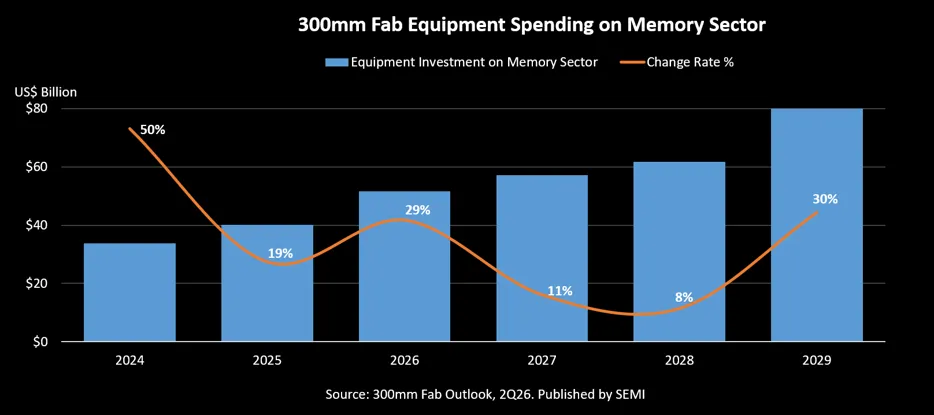
MILPITAS, Calif. – June 29, 2026 – Worldwide 300mm fab equipment investment in the memory sector is projected to surpass $50 billion for the first time in 2026, rising 29% to $52 billion before increasing another 11% to $57 billion in 2027, SEMI reported today in its latest 300mm Fab Outlook. The growth reflects continued AI-driven demand for advanced memory, supported by rising investment in AI infrastructure, data centers, and next-generation computing systems.

Looking further out, global 300mm fab equipment spending in the memory sector is expected to grow at a 19% CAGR from 2024 to 2029. Worldwide 300mm memory capacity is also projected to increase, reaching 4.1 million wafers per month in 2026 and 4.2 million wafers per month in 2027.

“Strong demand for high bandwidth memory and other advanced memory technologies is reshaping investment priorities across the semiconductor supply chain,” said Ajit Manocha, SEMI President and CEO. “As AI infrastructure expands, memory manufacturers are accelerating investments in both capacity and technology migration to support the next wave of data-intensive applications.”

Memory Segment Growth

The 2Q26 edition of the SEMI 300mm Fab Outlook includes an increased projection in 300mm fab equipment spending in the memory sector driven by continued upward capital expenditure plans among leading cloud service providers and strong demand for AI accelerators. DRAM equipment spending is expected to grow 29% to $37 billion in 2026, supported by strong HBM and DDR5 demand for GPUs and other AI accelerators. Equipment spending on 3D NAND is also projected to rise 28% to $14 billion in 2026, supported by increasing data storage requirements tied to AI deployment.

Continued investment in advanced-node DRAM and higher-layer 3D NAND is supporting a stronger memory capacity outlook, which has been revised upward in the 2Q26 edition of the SEMI 300mm Fab Outlook. Effective capacity growth, however, remains moderated by technology migration and process complexity, including advanced-node DRAM, HBM, and higher-layer NAND transitions.

The SEMI 300mm Fab Outlook lists 413 facilities and lines globally. The report reflects 155 updates and addition of 7 new fabs/lines projects since its last publication in March 2026. 

For more information on the report or to subscribe, please contact the SEMI Market Intelligence Team at [email protected]. More details are also available on the SEMI Market Data webpage.  

Follow SEMI Market Intelligence

Follow SEMI 

About SEMI

SEMI® is the global industry association connecting over 4,000 companies and 1.5 million professionals worldwide across the semiconductor and electronics design and manufacturing supply chain. We accelerate member collaboration on solutions to top industry challenges through Advocacy, Workforce Development, Sustainability, Supply Chain Management and other programs. Our SEMICON® expositions and events, technology communities, standards and market intelligence help advance our members’ business growth and innovations in design, devices, equipment, materials, services and software, enabling smarter, faster, more secure electronics. Visit www.semi.org, contact a regional office, and connect with SEMI on LinkedIn and X to learn more.  


RENA Technologies GmbH, a long-standing and experienced manufacturer of wet processing solutions for the semiconductor, advanced packaging, and solar industries, has been awarded a multi-million Euro order by a leading European semiconductor manufacturer for a specialized cleaning application designed for advanced substrates.

The solution is based on a high-performance batch wet processing platform and has been specifically engineered to deliver ultra-clean and highly efficient processing of demanding substrates. By combining advanced process control with a scalable batch architecture, the system ensures outstanding process stability, repeatability, and optimized throughput.

The customer’s decision underscores the technological strength and competitiveness of RENA’s wet processing solutions. Particularly when handling complex substrate materials, the application provides significant advantages in quality assurance, process control, and overall production efficiency. The mature cleanroom capabilities, excellent process control, and high- volume automation solutions of RENA add up to the perfect fit for the customer’s needs.

With this order, RENA further strengthens its position in the European semiconductor market and reinforces its commitment to delivering innovative, locally supported solutions to key industry players.

“Our success in securing this project highlights the growing demand for advanced wet processing technologies in Europe,” said Peter Schneidewind, CEO of RENA Technologies GmbH. “With more than 80 glass treatment tools in production worldwide - including cutting etch TGV/advanced packaging applications - RENA´s sophisticated technological solutions prove again in this new application for specialized semiconductor substrates.”

Date: May 8, 2026

Location: Drammen, Norway

Board-level and semiconductor test data are often analyzed separately, limiting correlation across the product lifecycle. Linking PCB assembly (PCBA) test results, including in-circuit and functional test, with upstream wafer, sort, and final test data remains difficult, particularly in photonics, advanced packaging, and high-density integration environments. yieldWerx and WATS announce a partnership to bridge this gap in the PCB test and semiconductor manufacturing workflows.

WATS is a test data management platform purpose-built for electronics manufacturers. It captures, standardizes, and analyzes high-volume test data from PCBA (printed circuit board assembly) production environments, including in-circuit test (ICT), functional test, and final test, giving engineers real-time visibility into board-level yield, anomalies, and quality metrics across the production line.

yieldWerx operates at the semiconductor level, connecting data across wafer fabrication, wafer sort, die, and packaged device test. Its enterprise analytics platform enables advanced yield analysis, traceability, and root cause investigation from design through silicon manufacturing.

Together, the platforms address the full product stack. This allows manufacturers to correlate PCBA-level signals with silicon quality data, improving visibility across test stages and enabling more effective analysis of yield and reliability issues.

Customer and industry benefits include:

Real-time PCBA test visibility for faster identification of yield and quality issues

Improved correlation between board-level test results and upstream chip or wafer data

Reduced time spent reconciling data across disconnected systems

Earlier detection of cross-stage patterns impacting yield and reliability

Faster root cause analysis spanning silicon, assembly, and board-level test

Better alignment between electronics manufacturing and semiconductor supply chain

The combined solution supports open architectures, APIs, and flexible deployment models, enabling integration without large-scale system changes.

About yieldWerx

yieldWerx is an enterprise analytics platform connecting data across the semiconductor product lifecycle, from design and wafer fabrication through wafer sort, die, and packaged device test, enabling advanced yield analysis, traceability, and data-driven decision-making across cloud, on-premises, and hybrid environments.

About WATS

WATS is a test data management and analytics platform developed by Virinco, built to collect, standardize, and analyze data from electronics manufacturing test systems. It provides real-time visibility into board-level performance across ICT, functional test, and final test operations, helping engineers monitor yield, detect anomalies, and improve quality at high volume.

Statements from Leadership
"We are excited to partner with yieldWerx. Our customers manufacture complex electronics where board-level test data alone only tells part of the story. By connecting PCBA production test data with yieldWerx's upstream semiconductor intelligence, we can give them a more complete picture of their product quality and yield." -- Tom Lomsdalen, CEO, Wats

“Our customers have been asking for a unified view that links semiconductor yield data with downstream electronics test results, and this partnership delivers exactly that. Together, yieldWerx and WATS empower engineering teams to move faster on root cause analysis, reduce escapes, and make smarter decisions across the entire product lifecycle.” -- Aftkhar Aslam, CEO, yieldWerx

For further information, please visit https://www.yieldWerx.com or https://www.Wats.com/.