downloadGroupGroupnoun_press release_995423_000000 copyGroupnoun_Feed_96767_000000Group 19noun_pictures_1817522_000000Member company iconResource item iconStore item iconGroup 19Group 19noun_Photo_2085192_000000 Copynoun_presentation_2096081_000000Group 19Group Copy 7noun_webinar_692730_000000Path
Skip to main content
Default Banner Image

semiconductor manufacturing

SEMI has long promoted the industry collaboration that has contributed to the rise of the smart digital world we live in today. A world where data is being generated continuously by systems, gadgets, and sensors around us – often referred to as the Internet of Things (IoT). In our personal lives, most of us have smartphones, smart watches, smart TVs and smart cars, and we live in smart homes and smart cities generating huge amounts of data.In the work world, data and analytics are now influencing almost every industry including healthcare, government, financial services, construction and transportation. This data has the potential to transform our lives and make our world even smarter – if we can communicate and process this data, and use it to come up with actionable recommendations or actions. Artificial Intelligence (AI) and Machine Learning (ML) techniques have generated much excitement precisely because they offer us ways to realize the full value of data by harnessing it and transforming it into active intelligence.Data-intensive technologies are required to store, communicate and analyze data. And it all starts with innovation in microelectronics chips and systems spanning processors, memory, sensors, radios and other devices, presenting a huge opportunity to producers of these technologies. However, with Moore's Law beginning to slow, technology paths and innovation options are diverging. Companies must swiftly assess these options in order to develop competitive offerings. But the technological complexity and divergence makes it increasingly expensive or even unaffordable for many companies to track and pursue these options.The good news is that cost-effective early assessment is possible through pre-competitive collaboration that can produce new and often unexpected cross-disciplinary insights by overcoming traditional silos in industry and academia. Unfortunately, important collaborative industry platforms, such as the International Technology Roadmap for Semiconductors (ITRS), have folded, opening a collaboration gap in the global microelectronics ecosystem.As part of its mission to help companies connect, collaborate, and innovate, SEMI has built a collaborative, cross-supply-chain platform – the Strategic Innovation Platform (SIP). The goal is to provide early and comprehensive assessment of future technologies that are five to eight years away from commercialization. The assessment identifies not just technical barriers but also manufacturing and supply-chain constraints to implementing new technologies. SIP brings together the entire microelectronics ecosystem including strategic technology thought leaders, subject matter experts, technology and application developers, academia, researchers, start-ups and government. With more than 2,100-member companies spread across the global electronics manufacturing supply chain, SEMI is uniquely positioned to enable this critical collaboration. Award-Winning First ProjectThe inaugural SIP project assessed key drivers of future technologies. A key finding was that fast, efficient interconnects between devices and components are critical to the system performance important to customers and users, implying that system-level optimization is required. For data-intensive applications, interconnects have emerged as a key bottleneck for both performance and power in various circuits and systems in part because the slowing of Moore’s Law has decelerated advances in individual device performance, and in part because systems are becoming more complex, requiring heterogeneous integration.To address this challenge, SIP brought together industry experts from ASE Inc., Dow Chemical, Lam Research, Qualcomm and Xilinx to assess the future impact of interconnects for data-intensive applications. SEMI also involved Stanford University professors to collaborate on modeling and simulation. Through this unique cross-disciplinary collaboration, SIP developed a realistic model to evaluate the system-level performance of single-chip systems, as well as multi-chip systems – including traditional 2D packages, high-performance 2.5D systems that use interposers, and futuristic 3D systems. SIP also explored supply chain challenges in business continuity, manufacturability, Environment, Health and Safety (EHS) and the regulatory environment. SEMI worked with a broad range of industry partners to ensure that the model parameters accurately reflected realities on the design and factory floors to ensure usable results. Experimentation has become ever more expensive, with one industry player reporting that “it costs us $100 million to do a good experimental evaluation.” Accurate models can go a long way toward reducing the cost of technology assessment. The SIP collaboration produced key quantifiable insights including comparisons that highlight the benefits and limitations of various materials being explored for future interconnects, and of architectures under consideration for future data-intensive applications. For example, the current workhorse for artificial intelligence (AI) platforms – 2.5D technology – delivers a 4X improvement over 2D packaging but falls short of providing the orders-of-magnitude improvement that future AI/ML applications may require. These findings enable the industry to begin to identify ways to optimize 2.5D architectures, transition to 3D heterogeneous integration for performance-critical applications in the medium term, and to eventually evaluate new paradigms such as neuromorphic and quantum. The project findings were presented late last year in the form of two research papers at Electronics System-Integration Technology Conferences (ESTC) and International Microelectronics Assembly and Packaging Society (IMAPS) recently. One received the “Best Paper of the Session” award at IMAPS – a recognition that affirms the power of a collaborative platform such as SIP to produce valuable insights to address the growing technology complexity within the microelectronics industry. The microelectronics industry is on the cusp of a historic inflection point, where it could fuel the rise of emerging applications in AI/ML and IoT, and can grow into a trillion dollar industry over the next several years. More importantly, the industry is poised to help solve some of society’s most complex problems in areas including healthy living, climate change and transportation. No company can do this alone, and pre-competitive platforms such as SIP are key both to accelerating innovation through cross-disciplinary collaboration, and to reducing costs for individual companies. Please contact Tom Salmon at [email protected] or Pushkar Apte at [email protected] for more details and to get involved in future projects.Tom Salmon is vice president of Collaborative Technology Platforms. Pushkar Apte is a strategic technology advisor at SEMI.
Read More
SEMI’s Environment, Health Safety (EHS) Advocacy program has been helping the semiconductor manufacturing supply chain collectively address common challenges for over 20 years. Now, as national and regional governments worldwide increasingly weigh legislation that could impact the industry, SEMI continues to ensure that microelectronics industry understands the potential impact and provides an effective platform for taking collective member-led action.Olivier Corvez recently joined SEMI to focus exclusively on shaping SEMI’s EHS Advocacy program to meet escalating demands on the industry. He recently sat down with SEMI’s communications team to discuss SEMI's evolving EHS Advocacy program. SEMI Communications: As senior manager of EHS Advocacy, based at SEMI’s Milpitas, California, headquarters, what do you see as the major issues impacting EHS Advocacy for electronics manufacturing worldwide?Corvez: EHS is a vast topic that cuts across many different types of issues such as regulatory compliance obligations, management systems performances, as well as sustainability related public disclosures. SEMI’s global members are engaged on all these fronts, while creating advanced materials, sophisticated tools and managing a complicated and extensive supply chain.On the regulatory side, there has been exponential growth in the number of EHS laws considered and adopted by legislatures worldwide. Often these new regulations generate shockwaves across the globe as member companies are required to adapt to new requirements that spread across the entire manufacturing supply chain.Many new regulations are originating from Europe and demand much of my attention. We are paying especially close attention to the Stockholm Convention on eliminating persistent organic pollutants. A chemical called PFOA has been a subject of much effort at SEMI for years now and we are heartened by the reception of our position by the European Commission.SEMI Communications: What do you find most interesting about operating the EHS Advocacy program at SEMI?Corvez: The first word that comes to mind is “variety.” This role involves a blend of strategy, regulatory interpretation skills, project management, communication and even accounting. There is always something new to learn and positions and strategies to develop.SEMI, as a member-driven, collaborative platform, needs a high level of knowledge sharing and communications. I am working to establish a workspace where members can share previously-created analyses and minimize “recreating the wheel.” We have ambitious plans to deploy additional tools and a redesigned website that will improve our knowledge-sharing capabilities and best serve our members.We also plan to renew collaboration with other industry associations such as SIA and SESHA. Partnering with other associations means our voice is stronger, our messaging is reinforced, and our efforts are coordinated. Last but not least, I believe that maintaining a sense of geographical proximity for SEMI’s worldwide efforts is important. SEMI’s local advocacy efforts are facilitated by SEMI regional staff and I look forward to collaborating with them as they maintain ongoing dialogue with our local members and their local, state and national governments. SEMI Communications: What is the most challenging part of your role?Corvez: The most challenging aspect will be to reinvigorate participation in all of our EHS activities and find ways to create a state of fruitful collaboration among members worldwide. Secondly, establishing a new EHS governance structure is a significant challenge, but it is incredibly important to have a strong leadership group and decision-making mechanism that will efficiently help define our vision and priorities.Our new direction will require members to lead our activities at all levels. We believe there is a strong ROI for companies to dedicate resources to address the issues or topics we need to pursue to keep them and their products, accepted, profitable and the industry to grow. While SEMI provides the platform for collaboration, we must supplement our efforts with members providing the manpower to ensure our activities are a success.SEMI Communications: Tell us about your background. Corvez: I bring 20 years of diverse experience as a consultant, auditor and corporate EHS program management across most economic sectors on a global scale. Recently, I managed an EHS team distributed across 10 countries, dedicated to providing EHS compliance support to Cisco facilities worldwide.In addition to compliance experience, I have worked on implementing EHS Management systems at ABB or Total while in France (primarily) in the late 1990s. While at KPMG in Paris I was involved in over 400 due diligence projects for transactions services for electronics, chemicals, auto industry, aeronautics, etc. On the sustainability reporting side, I was lucky to be involved with large corporations and spent five years verifying EHS and social performances disclosed in sustainability annual reports. I received my formal training and received a Masters of Science in Environmental Sciences from Universite de Rouen, France, and my Bachelors of Science in Environmental Geology from Northeastern University in Boston. I also trained as an ISO 14001 auditor at DNV Sweden.All of these experiences have led me to this current position at SEMI, where I look forward to making effective and meaningful impact.Have questions or suggestions for Olivier? He can be reached at [email protected] or at +1.408.943.6957. To learn more about the EHS advocacy program at SEMI, please click here.Heidi Hoffman is senior director of Technology Communities Marketing at SEMI.
Read More
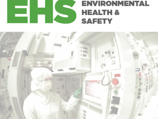
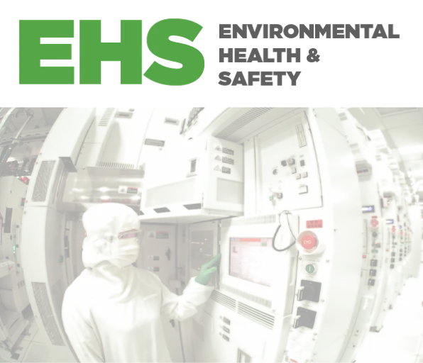
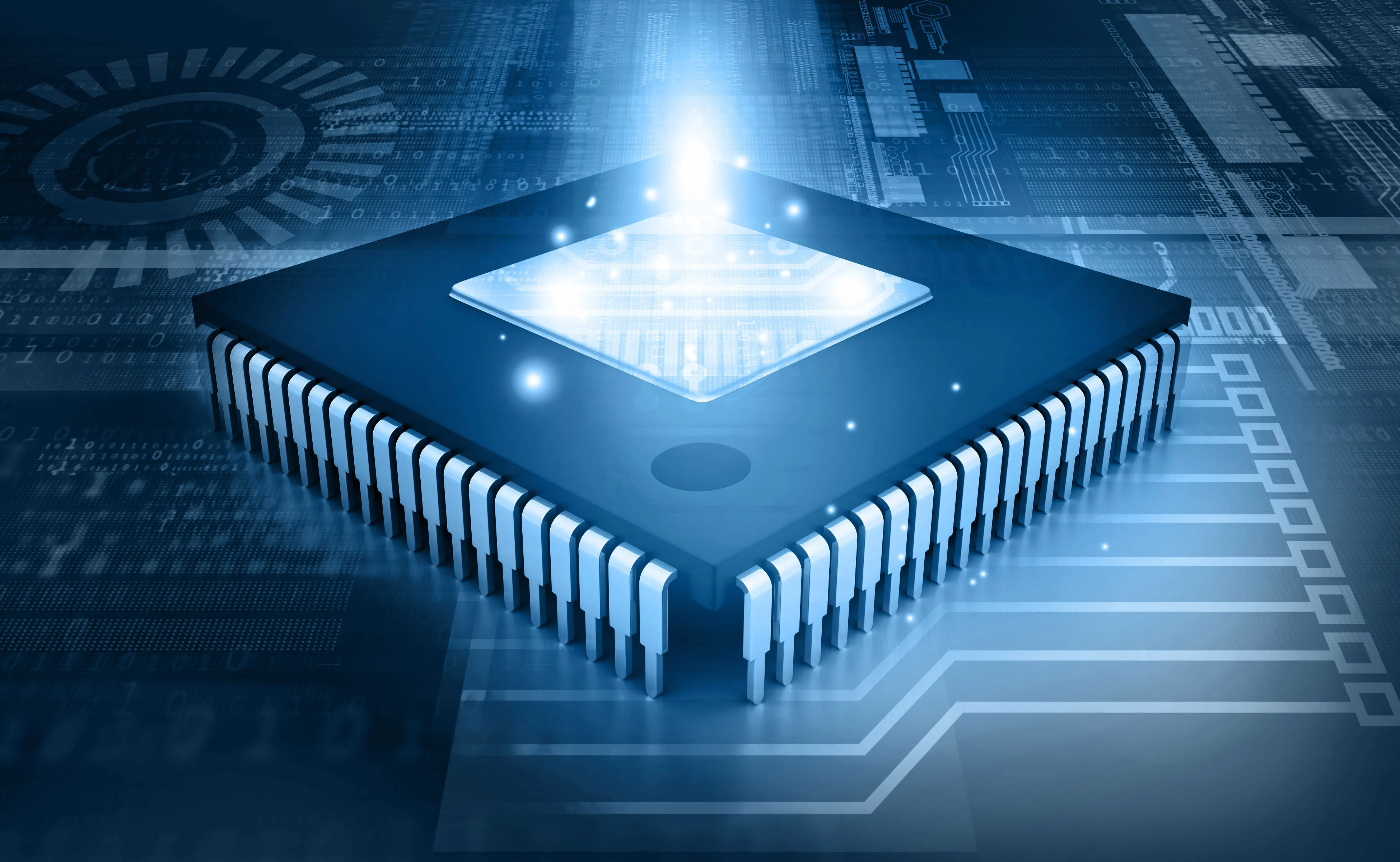
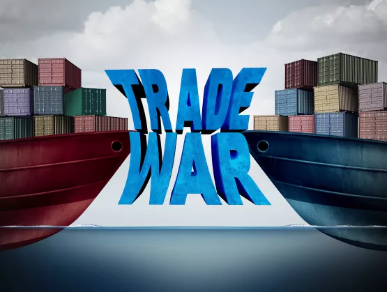
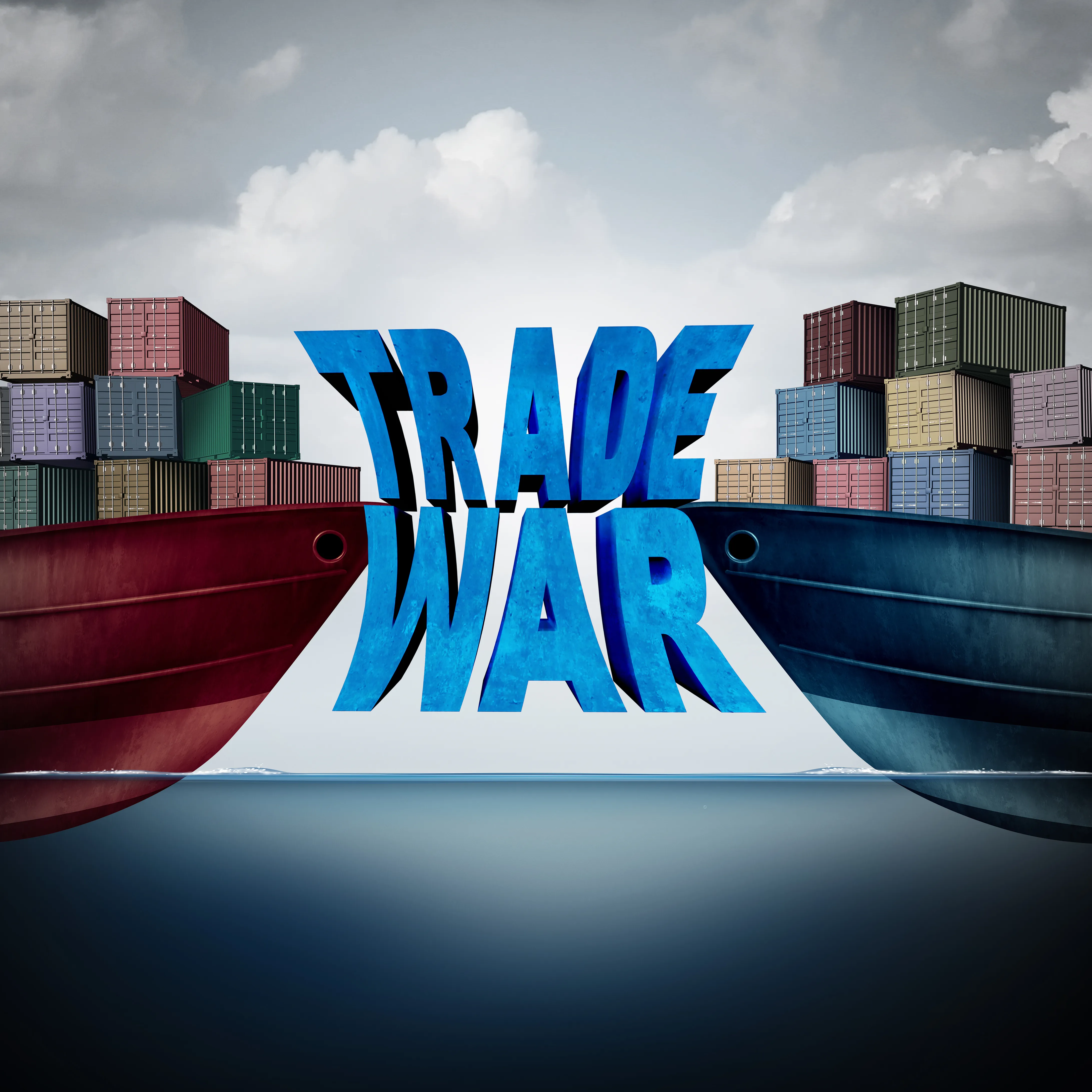
Last year the industry posted another remarkable double-digit revenue growth year. IC shipments eclipsed one trillion units for the first time and continued to enable an ever-expanding array of silicon intensive-applications.2018 was also a pivotal year of transformation at SEMI. Setting our sights firmly on building more value for SEMI members, we doubled down on priorities I established this time last year. We advocated intensively on global trade policies, industry talent needs, and critical environment, health and safety (EHS) concerns. To underpin our efforts around talent, we took the bold step to reinvigorate the industry’s identity with a dynamic image campaign. Above all, we targeted critical industry-wide issues to help us realize the ambition of becoming a trillion-dollar industry in the next decade. Workforce DevelopmentRedefining our approach to talent development in 2018 was and remains a top priority. A diverse, highly skilled workforce is crucial to the industry’s ability to innovate. Last year we ramped up a number of SEMI High Tech U (HTU) programs to inspire young people and attract them to careers in high-tech manufacturing. To date, more than 130,000 students have been touched by HTU – through student or teacher programs.Over the past year, we designed a new university outreach program and established partnerships with 100 institutions. We established Workforce Pavilions at SEMICON events in Southeast Asia, the U.S., Taiwan, Europe and Japan for students to explore career opportunities and meet with recruiters. We thrilled at seeing sponsors hire young talent at SEMI events. This year, all SEMICONs worldwide will feature Workforce Pavilions.SEMI also formalized its commitment to Diversity and Inclusion (D I) with the establishment of a D I council to shape new programs including the recently launched Spotlight on SEMI Women. To localize and fully optimize our D I programs, we established regional workforce councils in every region we serve. We unveiled the SEMI Mentoring Program to support students and young professionals on this journey by facilitating one-on-one mentoring relationships with industry professionals. Hundreds of mentees have enrolled. But we still need more mentors. I urge you to join the program. During the year, SEMI also expanded its workforce staff and developed a comprehensive workforce strategy with programs that engage students as early as elementary school and inspires them through high school and college. The program provides pathways to professional careers, building a pipeline to fill the short-term and long-term talent needs of the industry. Industry Image CampaignAs we developed the comprehensive workforce development program, we knew we had to refresh the industry’s image and appeal to the next generation through contemporary media and communications channels. So we recently launched a bold, innovative campaign to raise industry awareness and attract students and recent graduates to careers in semiconductor manufacturing.Our You’re Welcome campaign is a novel, creative approach that blends entertainment, media and storytelling to excite students about the industry. The campaign went viral immediately and within weeks had more than 5.5 million social media impressions and 2.3 million video views.Trade Policy AdvocacyRising trade tensions between the U.S. and China catapulted global trade policy to the forefront of industry concerns in 2018. Since the tariffs have taken force, semiconductor companies have faced higher costs, greater uncertainty, and difficulty selling products abroad. The tariffs have forced many SEMI member companies to pause or rethink their investment strategies.SEMI quickly engaged U.S. policymakers and provided resources for SEMI members. We formed a member trade task force, staged trade compliance seminars in China, and convened meetings with over 110 U.S. congressional, agency and administration officials, and provided testimony on the importance of the free trade to the industry.SEMI continues to educate policymakers about the critical importance of free and fair trade, open markets, and respect and enforcement of IP for all players in the global electronics manufacturing supply chain. As part of this initiative, we distributed “10 Principles for the Global Semiconductor Supply Chain in Modern Trade Agreements” and encouraged their adoption in various trade negotiations. These principles outline the primary considerations for balanced trade rules that benefit SEMI members around the world, strengthen innovation and perpetuate the societal benefits of affordable microelectronics.Environment, Health and SafetyEnvironmental regulations are proliferating globally even as advanced semiconductor manufacturing technology relies increasingly on a host of new materials. With dozens of new fabs and fab line upgrades, our industry must align on best practices, sensibly respond to materials restrictions, and renew efforts toward sustainable manufacturing.That’s why the revitalization of SEMI EHS efforts became another priority in 2018. Two months ago, we hosted the inaugural EHS Summit at SEMI Headquarters. Fully, 70 EHS professionals and company executives met to form the basis for the future SEMI EHS program.The Year AheadDespite a softening in the market, compounded by Apple’s first-ever announcement of a revenue decline in 16 years, a geopolitical whirlwind on trade and an extended shutdown of much of the U.S. government, the future is bright.At SEMI’s annual Industry Strategy Symposium (ISS 2019) in Half Moon Bay, Calif. in early January, the sense of optimism was palpable. In her keynote address, Dr. Ann Kelleher, Sr. VP and General Manager, Technology and Manufacturing Group, at Intel, observed that data is powering the fourth industry revolution and the expansion of compute. With customers expecting continual improvements in applications, Kelleher highlighted the tremendous opportunity for the chip industry to meet these expectations.At ISS 2019, we announced a Memorandum of Understand between SEMI and imec. The MOU will enable us to accelerate our members’ engagement in SEMI’s Smart vertical market platforms, in particular Smart MedTech and Smart Transportation. Our partnership with imec will also allow us to boost SEMI Standards activities in non-CMOS technologies, deepen technology roadmap efforts and augment our SEMI Think Tank initiative in thought leadership at a global level.Over the course of this coming year, will we begin our global rollout of key building blocks of our comprehensive workforce development program to engage schoolchildren as young as 10 and learners all the way to veterans who return to the workforce. We are now able, with the invaluable help of our Workforce Development Council and the passionate engagement of many SEMI member companies, to offer a solution to the talent crisis in our industry.We will continue to be the leading voice for our members and the end-to-end semiconductor supply chain across Talent, Trade, Tax and Technology as we work to ensure free, fair trade that protects IP while preserving vital access to markets to grow the supply chain. Vertical Market PlatformsOur vertical market platforms are an important part of this growth. For example, in Smart MedTech, SEMI looks forward to working with the Nano-Bio Materials Consortium to advance human monitoring technology for telemedicine and digital health after winning $7 million to fund the renewed program. In Smart Transportation, we will leverage the Global Automotive Advisory Council (GAAC) we formed last year to represent the full automotive supply chain and the Smart Transportation and Smart Automotive forums featured at all our SEMICON events to enable the industry to identify and seize opportunities in autonomous driving. At ISS 2019, Sujeet Chand of Rockwell Automation noted that “digitization will grow faster in the next 10 years than it did in the past 50,” a trend calling for semiconductor fab architectures that transform data into business value. We will continue to bring the industry together at our Smart Manufacturing venues to help uncover ways to deploy deep learning, edge computing and other Smart technologies to deliver this value and meet the challenges of automation as artificial intelligence’s (AI) sprawling influence reshapes industries including manufacturing.I am filled with optimism and thrilled about the opportunities I see on the horizon for our members as we build on our 2018 accomplishments to enable your prosperity in 2019 and beyond. My heartfelt thanks to all of you for your participation in our programs and events.I look forward to another successful year as we connect, collaborate and innovate together!Ajit Manocha is president and CEO of SEMI.
Read More
Environment, Health and Safety (EHS) has steadily evolved to become a key element within SEMI’s Advocacy and Standards activities. On November 29th, 2018, nearly 60 members representing equipment, materials and device manufacturers gathered at SEMI’s Milpitas headquarters for our first EHS Summit. The main agenda for the day was related to discussing the new “EHS 2.0” strategy – and priorities – to better align with the current landscape facing members in various parts of the world. “SEMI will not compromise our commitment to EHS,” said SEMI president and CEO Ajit Manocha in is kickoff speech at the Summit, calling on members to rise to the challenge. “We also understand the importance of EHS for our industry. SEMI EHS staff is here to facilitate a program that achieves the highest priorities of our members – but we need you, our members, to be clear on your priorities.” SEMI’s EHS program has had many successes globally, including a strong suite of safety standards, since it launched in the 1980’s. Since then, exponential growth of EHS regulatory requirements worldwide has intensified pressure on members to become more transparent on environmental and social issues. The pressure to disclose on EHS performances has become more visible and challenging for members to manage across the entire supply chain. During facilitated breakout sessions, members were invited to share their views on various industry issues. Some of the most pressing raised related to changes in the REACH European Regulations, or implications from the Stockholm Convention that will affect what products or hazardous chemicals can be used. Some of the topics identified throughout the day included: Circular economy/green/sustainability Global RoHS and REACH regulations Used equipment machine safety Current and future prohibited substances tracking such as Perfluorooctanoic acid (PFOA) After the summit’s success, SEMI is now planning three EHS summits in 2019 and other events to further address the various issues facing members. To receive invitations and stay abreast of SEMI’s EHS activities, please join our EHS interest list by clicking here. Olivier Corvez is senior manager of Environment, Health, Safety and Sustainability at SEMI.
Read More
Even for someone who has been in this industry since the days of the TI Datamath 4-function calculator and the TMS1100 4-bit microcontroller (yes, that’s been a LONG time – the movie Grease premiered the same year!), it is sometimes hard to grasp the scope and complexity of what happens in today’s leading-edge semiconductor gigafabs. In fact, the only way to comprehend the enormous volume of transactions that occur is to consider what happens in a single minute – this is illustrated in the infographic we have labeled “The Gigafab Minute.”* It’s amazing enough to think that a single factory can start 100,000 wafers every month on their cyclical journey through 1500 process steps… and have 99%+ of them emerge 4 months later to be delivered to packaging houses and then on to waiting customers. It’s quite another to realize that all of this happens continuously (24 x 7) and automatically. “How is this possible?” you ask.Well, a big part of the solution is the body of SEMI standards which have evolved since the early 80s to keep pace with the ever-changing demands of the industry. From an automation standpoint, many of these standards deal with the communications between manufacturing equipment and the factory information and control systems that are essential for managing these complex, hyper-competitive global enterprises.A significant characteristic of these standards is that they have been carefully designed to be “additive.” This means that new generations of SEMI’s communications standards do not supplant or obsolete the previous generations, but rather provide new capabilities in an incremental fashion. To appreciate the importance of this in actual practice, consider how the GEM, GEM300, and EDA/Interface A standards support the transactions that occur in a single Gigafab Minute.Starting at 1:00 o’clock on the infographic and moving clockwise, you first notice that 2.31 wafers enter the line. Of course, these are actually released in 25-wafer 300mm FOUPs (Front-Opening Unified Pod), but 100K wafers per month translates to 2.31 per minute. Since these factories run continuously, once the line is full, it stays full. And with an average total cycle time of 4 months, this means that there are 400K wafers of WIP (work in process) in he factory at any given time. This number, and the total number of equipment (5000+), drive the rest of the calculations.GEM (Generic Equipment Model) – SEMI E30, etc.The GEM messaging standards were initially defined in the early 90s to support the factory scheduling and dispatching applications that decide what lots should go to what equipment, the automated material handling systems that deliver and pick-up material to/from the equipment accordingly, the recipe management systems that ensure each process step is executed properly, and the MES (Manufacturing Execution System) transactions that maintain the fidelity of the factory system’s “digital twin.”Every minute of every day, GEM messages support and chronicle the following activities: 240 process steps are completed (i.e., 240 25-wafer lots are processed), 300 recipes are downloaded along with a set of run-specific adjustable control parameters, and 600 FOUPs are moved from one place to another (equipment, stockers, under-track storage, etc.). For each of these activities, the factory’s MES is notified instantaneously.GEM300 – SEMI E40, E87, E90, E94, E157With the advent of 300mm manufacturing in the mid-to-late 90s, a global team of volunteer system engineers from the leading chip makers defined the GEM300 standards to support fully automated manufacturing operations. Starting at 5:00 o’clock on the infographic, the number of transactions per minute jumps almost 3 orders of magnitude, from the monitoring of 900 control jobs across 4000 process tools to the tracking of 360,000 individual recipe step change events. This level of event granularity is essential for the latest generation of FDC (Fault Detection and Classification) applications, because precise data framing is a key prerequisite for minimizing the false alarm rate while still preventing serious process excursions. In this context, more than 6000 recipe-, product- and chamber-specific fault models may be evaluated every minute.Simultaneously, the applications that monitor instantaneous throughput to prevent “productivity excursions” and identify systemic “wait time waste” situations depend on detailed intra-tool wafer movement events. In a fab with hundreds of multi-chamber, single-wafer processes, 75,000 or more of these events occur every minute. EDA (Equipment Data Acquisition) – SEMI E120, E125, E132, E134, E164, etc.Rounding out the SEMI standards in our example gigafab is the suite of EDA standards which complement the command and control functions of GEM/GEM300 with flexible, high-performance, model-based data collection. The EDA standards enable the on-demand collection of the volume and variety of “big data” required from the equipment to support the advanced analysis, machine learning, and other AI (Artificial Intelligence) applications that are becoming increasingly prevalent in leading semiconductor manufacturers. As EUV (Extreme Ultraviolet) lithography moves from pilot production to high-volume manufacturing at the 7nm process node and beyond, the litho process area will become a major source of process data by itself, generating 10 GB of data every minute. This is in addition to the 100 GB of data collected from other process areas. The End ResultThe final wedge (12:00 o’clock) in our infographic highlights the real objective – which is producing the millions of integrated circuits that fuel our global economy and provide the technologies that are an integral part of our modern way of life. Assuming a nominal die size of 50 square mm (typical of an 8 GB DRAM), the 2.31 wafers we started at 1:00 o’clock result in almost 3200 individual chips. But none of this would be possible without the pervasive factory automation technology we now take for granted. So, as you finish reading this posting on whatever device you happen to be using, take a micro-moment to acknowledge and thank the hundreds of standards volunteers whose insights and efforts made this a reality!You may not be responsible for running a gigafab anytime soon, but the SEMI standards used in this setting are no less applicable to any Smart Manufacturing environment. Give us a call if you’d like to know more about how these technologies can benefit your operations for many years to come.Alan Weber is Vice President, New Product Innovations, at Cimetrix Incorporated. Previously he served on the Board of Directors for eight years before joining the company as a full-time employee in 2011. Alan has been a part of the semiconductor and manufacturing automation industries for over 40 years. He holds bachelor’s and master’s degrees in Electrical Engineering from Rice University. For more information on SEMI Standards, please click here.
Read More
Tensions between the U.S. and China have reached fever pitch as the Trump administration imposed higher tariffs on $200 billion of Chinese goods last Monday, adding to the $50 billion in goods hit with higher duties earlier this year. Bloomberg News reported that “the combined $250 billion in products facing levies is almost half the value of imports from China last year.”China countered by meting out stiffer tariffs on $60 billion in U.S. goods, on top of the $50 billion already levied, and canceling planned trade negotiations with the Trump administration.Days before the sharp escalation of the trade conflict, SEMI president and CEO Ajit Manocha joined SEMI China president Lung Chu in hosting a closed-door round table with 16 senior semiconductor industry executives in Shanghai. The goal: An update from the China semiconductor sector on its needs as the chip industry braces to weather the conflict. Manocha and Chu then met with influential China media outlets including Semiconductor Manufacturing, China Integrated Circuit, Silicon Semiconductor and IC Café to reiterate SEMI’s position on trade.“The basic principles of SEMI are free and fair trade, open markets, cooperation for mutual benefit, and protection of intellectual property rights,” Manocha told the reporters. “Tariffs and trade frictions are bound to harm the industry’s development.”Manocha highlighted efforts over the past few months by the SEMI advocacy team to educate U.S. policymakers on the impact of tariffs on the development of the semiconductor industry. Last month, the office of the U.S. Trade Representative (USTR) held a hearing in Washington, D.C. to solicit public comment on then-proposed tariffs on $200 billion of Chinese imports to the U.S. Testifying on behalf of the semiconductor industry, SEMI stressed that tariffs on more than 100 tariff lines covering items critical to semiconductor manufacturing “will harm companies in the semiconductor supply chain by increasing business costs, introducing uncertainty, and stifling innovation.” SEMI had testified twice before this year – the first time in May, opposing levies on $34 billion in Chinese goods, and the second in July to speak out against higher duties on $16 billion worth of Chinese products.SEMI China president Lung Chu made clear the consensus of China’s semiconductor sector: The trade war will profoundly impact the global semiconductor industry. He also stressed that SEMI, as a global industry organization linking the global electronic semiconductor industry chain, will continue to promote win-win cooperation between the U.S. and China.Manocha reaffirmed SEMI’s longstanding commitment to promote cooperation among nations and policies that foster industry growth.“For the growth of the semiconductor industry, SEMI is focused on four important factors, and we call them the 4 T’s, namely Tax, Technology, Talent, Trade,” Manocha told the media. “All are indispensable for the development of the industry.” SEMI president and CEO Ajit Manocha and SEMI China president Lung Chu host press conference in Shanghai.Because the semiconductor industry is international, with key features spread across a number of regions, cross-border cooperation is an eternal theme, Chu told the gathering. To maintain the vitality of China's semiconductor industry, the region must deepen its integration with the international semiconductor ecosphere. He acknowledged that there will be no quick answers to easing trade tensions between the U.S. and China but that SEMI would continue to press ahead in efforts to help improve relations. Despite the conflict, the industry remains optimistic about the growth of China’s semiconductor industry, he said."However, we need to face up to the fact that there is still a certain gap between the domestic semiconductor industry and that of international advanced level,” Lu said. “Therefore, international cooperation is the key to industry growth."Of the four cornerstones of the semiconductor industry – design, manufacturing, testing and equipment materials – China in recent years has narrowed the gap with its international counterparts in testing capabilities, Chu said. For China’s semiconductor industry to flower, the region must build strengths in design, manufacturing and materials too.“The semiconductor industry needs long-term investment, persistence and patience, and also needs win-win cooperation, continuous innovation and product applications across the entire industry,” Chu said. “Money is not the only incentive.”Manocha emphasized the theme of international cooperation, with the global semiconductor industry working in harmony.“The global semiconductor industry chain is inseparable, and each region has its own advantages,” Manocha said. “So, we will continue to work hard to create a win-win, inclusive global industrial atmosphere.”For its part, SEMI China is focused on becoming the best partner for China to realize its semiconductor dream by continuing to provide services that encourage international cooperation. That role will grow in importance with SEMI’s expansion into application areas such as smart manufacturing, smart transportation, smart data and smart automotive – all requiring tighter integration of the electronics industry supply chain.Cherry Sun is a marketing manager at SEMI China.
Read More
U.S. Government Imposes Tariffs on $200 Billion of Goods and China Retaliates on $60 Billion of GoodsEarlier this week, the U.S. Trade Representative (USTR) released a 10 percent tariff on $200 billion in imports from China, including more than 90 tariff lines central to the semiconductor industry.The 10 percent tariff will take effect on September 24, 2018, and rise to 25 percent on January 1. These tariff lines will cost SEMI’s 400 U.S. members tens of millions of dollars annually in additional duties. However, counting the products included in the previous rounds of tariffs, the total estimated impact exceeds $700 million annually. China has already announced that it will respond with tariffs on $60 billion worth of U.S. goods. In his notice, President Trump said the U.S. will impose tariffs on $267 billion worth of goods if China retaliates. The U.S. government removed 279 total tariff lines, including three lines that impact our industry: silicon carbide, tungsten, and network hubs used in the manufacturing process.As we’ve noted, intellectual property is critical to the semiconductor industry, and SEMI strongly supports efforts to better protect valuable IP. However, we believe that these tariffs will ultimately do nothing to address the concerns with China’s trade practices. This sledgehammer approach will introduce significant uncertainty, impose greater costs, and potentially lead to a trade war. This undue harm will ultimately undercut our companies’ ability to sell overseas, which will only stifle innovation and curb U.S. technological leadership.Product Exclusion Process – List 2USTR formally published the details for the product exclusion process for products subject to the List 2 China 301 tariffs (the $16 billion tariff list). If your company’s products are subject to tariffs, you can request an exclusion.In evaluating product exclusion requests, the USTR will consider whether a product is available from a source outside of China, whether the additional duties would cause severe economic harm to the requestor or other U.S. interests, and whether the product is strategically important or related to Chinese industrial programs (such as “Made in China 2025”).The request period ends on December 18, 2018, and approved exclusions will be effective for one year, applying retroactively to August 23, 2018. Because exclusions will be made on a product basis, a particular exclusion will apply to all imports of the product, regardless of whether the importer filed a request.More information, including the process for submitting the product exclusion request and details what information should be included in your submission can be found here. Please let me know if your company plans on filing an exclusion. SEMI has prepared a document that includes guidelines for your exclusion filing, an explainer on how to submit, and links to official government info. SEMI is glad to assist your companies file exclusion requests for your products. SEMI will continue tracking ongoing trade developments. Any SEMI members with questions should contact Jay Chittooran, Public Policy Manager at SEMI, at [email protected].
Read More
Storage and memory chipmaker and SEMI China member Tsinghua Unigroup is gearing up to meet burgeoning product demand with huge investments in its manufacturing plants. But the high-tech enterprise under Tsinghua University is eyeing a much bigger prize – growth of the region’s semiconductor industry and the realization of its ambition to become a more prominent force on the global stage.Inspired by the national strategy, the Tsinghua Unigroup’s big spends include USD 24 billion in Wuhan (Yangtze Memory Technologies Co., Ltd.,) USD 30 billion in Chengdu, USD 30 billion in Nanjing and USD 100 billion in Chongqing, said Liu Hongyu, senior vice president of Tsinghua Unigroup, speaking at the SEMI China Equipment and Materials Committee meeting last month.Advanced packaging is another rich vein of opportunity the region is tapping for expansion, said Liu Hongjun, vice president of China Wafer Level CSP Co., Ltd., another SEMI China member attending the event, hosted by NAURA in Beijing. Hongjun sees strong growth for Fan-in, Fan-out, FCBGA, 2.5D and 3DIC, with Fan-out out front. Liang Sheng, administrative commission director at BDA, a business advisory firm supporting high-technology manufacturing in the E-Town economic development zone, pointed to 5G chips and smart, networked electric automobiles as drivers of the next growth phase of Beijing’s integrated circuit (IC) industry.Global tailwinds are lifting China’s semiconductor industry and the region’s hopes, with SEMI and major industry analysts raising their semiconductor industry growth projects for 2018 to between 9 percent and 16 percent. According to SEMI’s latest market report, global semiconductor industry manufacturing equipment revenue reached USD 17 billion in the first quarter of 2018, logging all-time highs after jumping 12 percent from the previous quarter and 30 percent year-over-year. Korea was the top-performing region at USD 6.26 billion, followed by China at USD 2.64 billion.Tighter integration with the rest of the global semiconductor industry is critical to the growth of China’s chip sector, and SEMI China is squarely focused on this assimilation, said SEMI China president Lung Chu. The spearhead of this effort is the SEMI Innovation Investment Platform (SIIP) China, established by SEMI China last year to help grow China’s pool of skilled workers, promote advanced technology, generate industry capital, and expand China’s semiconductor industry while developing stronger connections with chip sectors in other regions. To strengthen ties with other regions, SIIP China will stage a number of innovation and investment forums this year including Chinese Night at SEMICON West (July 10-12) and a SIIP China Forum in Silicon Valley (July 15). In August, representatives from the Korea chip industry will visit counterparts in China (August), and a China delegation will travel to Japan for meetings (October). SIIP China is also strengthening the region’s links with Germany and Israel as SEMI serves as a crucial bridge between China’s semiconductor sector and the global industry.At the invitation of Shanghai authorities and the Ministry of Commerce of the People’s Republic of China, SEMI China in November will join the China International Export Import Exposition in Shanghai, an event that will underscore China’s commitment to the openness and cooperation of its semiconductor industry with the international chip community. As part of the exposition, SEMI will work with the Ministry of Commerce and domestic chip manufacturers to begin development of a special integrated circuit (IC) zone. SEMI China members are welcome to participate.With workforce development no less vital to the future of China’s semiconductor industry, the Equipment Materials Committee offered potential solutions to the industry’s talent gap. Measures included targeting university students and engineers with industry lectures and courses in key cities, campus recruiting, talent training that members said they are willing to help SEMI coordinate and stage and, much like the push to better integrate China with the global semiconductor industry, mobilizing member resources around a campaign to polish the image of the industry to make it more attractive to students and young workers. Members of the SEMI China Equipment Material Committee gathered at NAURA in Beijing in June for a warm and lively discussion about global semiconductor industry cooperation and growing China’s semiconductor sector.Cherry Sun is a marketing manager at SEMI China.
Read More
Testifying before a U.S. interagency panel weighing trade tariffs against China, Jonathan Davis, global vice president of industry advocacy at SEMI, yesterday called for the removal of more than 100 products from the list of tariffs proposed by the Trump administration, stressing that an escalation of the U.S.-Sino dispute could trigger a full-blown trade war and hasten deep, unintended damage including higher consumer prices, an expanded U.S. trade deficit, and a slowdown in U.S. economic growth.Representing the electronics manufacturing supply chain, Davis threw the industry’s weight behind protections for valuable intellectual property but argued that “if implemented as proposed, these tariffs will potentially cost tens of millions annually in additional taxes and lost revenue owing to reduced exports, threaten thousands of high-paying U.S. jobs, and not solve U.S. concerns with China.” Davis said the undue harm will ultimately undercut the ability of U.S. chipmakers to sell overseas, stifling innovation and curbing U.S. technological leadership.In testimony at the hearing before the government panel that included representatives from the U.S. Trade Representative (USTR), Departments of Treasury, Commerce, State and Defense, and the Council of Economic Advisers, Davis explained that more than 100 lines – products defined for the purpose of setting import duties – of the proposed tariffs would hamstring the semiconductor supply chain. The tariff lines include fundamental components of the semiconductor manufacturing process that are oxygen for the chip industry. As part of his testimony, Davis also submitted comments on the impact of the tariffs.Charles Gray, general counsel at Teradyne, who also testified at the hearing, said the tariffs will threaten growth while penalizing U.S. companies with supply chains that touch China. Gray and Davis were among more than 100 industry leaders who provided more than 3,000 comments in the May 15-17 hearing to evaluate the impact and efficacy of the proposed tariffs.The hearing followed the Trump administration’s heated, longstanding criticism of China for what it considers unfair trade practices, focusing specifically on intellectual property violations. In recent months, the administration has begun implementing trade actions against China that will increase tariffs, restrict cross-border investment, and introduce significant uncertainty for U.S. businesses.The Section 301 investigation that determined China’s forced transfer of technology and intellectual property discriminated against U.S. firms prompted a proposed 25 percent tariff on $50 billion in U.S. imports from China – a punitive measure that would squarely hit the semiconductor manufacturing industry.SEMI continues to educate policymakers on the deep damage tariffs would exact on the long-term health of the semiconductor industry and the critical importance of balanced trade to the future of the semiconductor industry.For more information on trade or how to participate in SEMI’s public policy program, please contact Jay Chittooran, SEMI public policy manager, at [email protected].
Read More