Showing 265 - 276 of 11482
Blog
Silicon Provenance: Building Trust Through Traceability, Authenticity, and Lifecycle Auditability
At SEMICON West, Prabhu Jayanna from AMD presented a compelling vision for how the semiconductor ecosystem can strengthen trust in the devices it produces. His focus was silicon provenance—a...
Blog
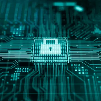
Stopping Counterfeits with Physics: Inside the Future of Semiconductor Fingerprinting
At SEMICON West, Dr. Bertrand Cambou of High Entropy Security explored a fast-evolving challenge in the semiconductor ecosystem: the rise of counterfeit and cloned devices. His session introduced a...
Blog
Navigating Global OT Cybersecurity Regulations: What Semiconductor Leaders Must Know
At SEMICON West, experts from Sun Square, Moxa, and NY CREATES underscored a pivotal reality: regulatory pressure in the semiconductor industry has reached a historic tipping point. For the first...
Blog
Sensing Tomorrow: Emerging Applications for MEMS & Sensor Technologies
At SEMICON West, the SEMI MEMS and Sensors Industry Group (MSIG) showcased how advances in sensor miniaturization, integration, and edge intelligence are reshaping mobility, automation, and the...
Blog
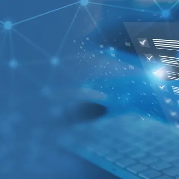
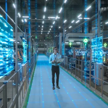
Building the Digital Twin Backbone: Why Scalable Data Platforms Are No Longer Optional
At SEMICON West, industry leaders agreed: Scalable, secure data platforms are now essential for AI-driven semiconductor manufacturing. Federated data sharing, traceability, and edge-to-cloud...

Blog
Imaging Across Assembly and Test: Enabling Manufacturable Complexity
Insights from SEMICON West APHI Sessions On Advanced Package Assembly, Test Visibility, and Closed-Loop ManufacturingThe Advanced Imaging sessions highlighted imaging’s expanding role beyond...

Blog
From Inspection to Intelligence: Imaging as a Driver of AI-Era Manufacturing
Insights from the SEMICON West Session “Reimaging and Transforming Package Assembly and Test Manufacturing in the AI Era”Across the Advanced Imaging track, speakers consistently described imaging’s...

Blog
When Materials Meet Imaging: Dielectrics as a Defining Constraint
Insights From APHI Sessions Exploring The Interaction Between Advanced Materials, Imaging Fidelity, and ReliabilityAdvanced Imaging sessions at SEMICON West underscored a subtle but critical shift:...
Blog
Advanced Imaging: A Foundational Enabler for AI-Era Semiconductor Packaging
Insights from SEMICON West APHI Sessions on Advanced Imaging, Heterogeneous Integration, and Manufacturability at Scale.At SEMICON West, the Advanced Imaging sessions reinforced a pivotal industry...
Article
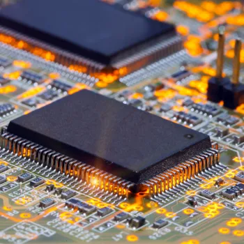
Technical Deep Dive: Devices, Materials, and Manufacturing for Sustainable AI
As AI workloads continue to scale, gains in performance and efficiency are increasingly determined by physical design choices at the device, materials, and manufacturing levels. This technical deep...