
Insights from SEMICON West APHI Sessions On Advanced Package Assembly, Test Visibility, and Closed-Loop Manufacturing
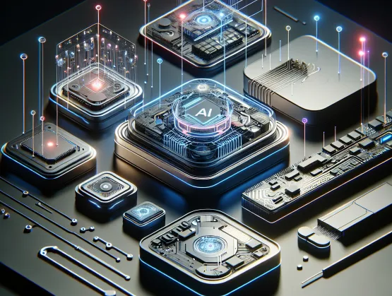
The Advanced Imaging sessions highlighted imaging’s expanding role beyond lithography and inspection into assembly and test—areas now central to advanced packaging success. As packages incorporate multiple dies, advanced interconnects, and heterogeneous materials, imaging provides critical visibility into structures that electrical test alone cannot fully characterize.
Speakers emphasized that imaging closes the gap between design intent and physical execution.
Making Complexity Manufacturable
Advanced packages demand precise alignment, bonding integrity, and structural consistency across hidden interfaces. Imaging enables non-destructive verification throughout assembly, helping identify issues early and reducing costly downstream failures.
Several presenters noted a shift toward in-line imaging during assembly, allowing manufacturers to intervene sooner and shorten learning cycles.
Closing the Feedback Loop
Imaging data from assembly and test increasingly feeds upstream into design, materials selection, and process optimization. This closed-loop approach accelerates yield maturity—an essential requirement given the cost and performance expectations of AI devices.
Why It Matters
- Assembly and test complexity continues to rise
- Imaging reveals issues invisible to electrical test
- Feedback loops improve yield, reliability, and time-to-market
What to Watch
- Greater in-line imaging during assembly
- Integration of imaging and test data
- Imaging-informed design-for-manufacturability workflows
Source: “Afternoon Session: Building and Scaling AI: From Design to Productization,” SEMICON West 2025. Speakers: Ravi Mahajan (Intel); William Chen (IEEE EPS); PR Chidambaram (Qualcomm); C.P. Hung (ASE); Tim Lee (Boeing & IEEE); Ming Li (Lam Research); Jeff Pettinato (Intel Corporation). Panel moderator: Audrey Charles (Lam Research). Panelists: C.P. Hung (ASE); Tim Lee (Boeing & IEEE); Jeff Pettinato (Intel Corporation); Ming Li (Lam Research); PR Chidambaram (Qualcomm).


