
Insights from SEMICON West APHI Sessions on Advanced Imaging, Heterogeneous Integration, and Manufacturability at Scale.
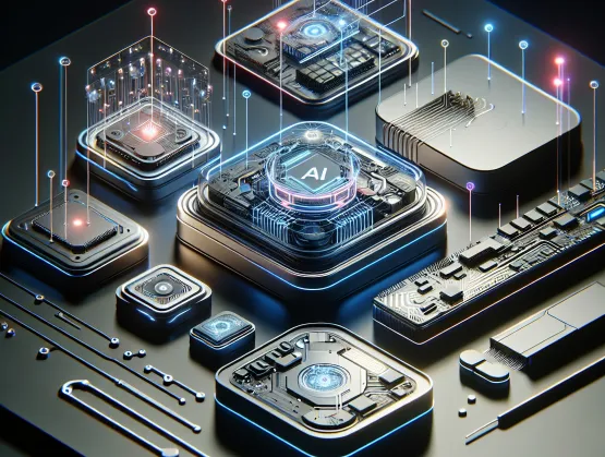
At SEMICON West, the Advanced Imaging sessions reinforced a pivotal industry shift: imaging has moved from a supporting manufacturing function to a strategic enabler of AI-driven semiconductor innovation. As architectures evolve toward chiplets, heterogeneous integration, and complex 2.5D and 3D structures, imaging now underpins performance, yield, scalability, and ultimately time-to-market for AI systems.
Across the sessions, industry leaders emphasized that advanced packaging innovation cannot outpace imaging capability. Without corresponding advances in resolution, scale, data fidelity, and integration, even the most ambitious architectures risk stalling before high-volume production.
Imaging Must Evolve with Architectural Ambition
Advanced packaging architectures introduce fundamentally new manufacturing realities: larger substrates, tighter interconnect pitches, heterogeneous material stacks, and non-planar surfaces. Imaging systems are now expected to deliver consistent precision across warped panels, multi-die assemblies, and mixed materials—often at scales well beyond traditional wafer formats.
Several speakers highlighted that imaging innovation is no longer about incremental gains. Instead, it is about enabling manufacturability at system scale—bridging the gap between architectural intent and factory execution.
From Manufacturing Step to Strategic Capability
A recurring theme was the repositioning of imaging from a downstream inspection step to an upstream design and process enabler. Imaging data increasingly feeds AI-driven control loops, yield-learning platforms, and digital twins, allowing fabs to anticipate issues rather than react to failures.
This evolution positions imaging as a connective tissue across design, materials, process, and assembly—supporting faster learning cycles and more resilient manufacturing flows.
Why It Matters
- Advanced packaging success depends on imaging precision at unprecedented scale
- Imaging data is foundational to AI-enabled manufacturing strategies
- System-level innovation stalls without imaging alignment
What to Watch
- Imaging platforms designed explicitly for heterogeneous integration
- Deeper coupling between imaging systems and AI analytics
- Industry collaboration to standardize imaging data pipelines
Source: “Afternoon Session: Building and Scaling AI: From Design to Productization,” SEMICON West 2025. Speakers: Ravi Mahajan (Intel); William Chen (IEEE EPS); PR Chidambaram (Qualcomm); C.P. Hung (ASE); Tim Lee (Boeing & IEEE); Ming Li (Lam Research); Jeff Pettinato (Intel Corporation). Panel moderator: Audrey Charles (Lam Research). Panelists: C.P. Hung (ASE); Tim Lee (Boeing & IEEE); Jeff Pettinato (Intel Corporation); Ming Li (Lam Research); PR Chidambaram (Qualcomm).


