downloadGroupGroupnoun_press release_995423_000000 copyGroupnoun_Feed_96767_000000Group 19noun_pictures_1817522_000000Member company iconResource item iconStore item iconGroup 19Group 19noun_Photo_2085192_000000 Copynoun_presentation_2096081_000000Group 19Group Copy 7noun_webinar_692730_000000Path
Skip to main content
Default Banner Image

Technology and Trends

The semiconductor industry is hitting a structural inflection point: explosive AI‑driven demand, rapidly rising manufacturing complexity, and stringent sustainability expectations are converging at once. In this context, edge AI deployed directly on tools, sensors, and local controllers, is shifting from experimental to essential, particularly in fabs where milliseconds matter. SEMI’s timely workshop, Smarter Sensors, Smarter Fabs: AI at the Edge in Semiconductor Manufacturing, taking place March 18–19, 2026 in Milpitas, CA, will address this important topic.From sparse sensing to dense instrumentationTwo decades ago, most process tools relied on dozens of sensors per chamber. Today, leading etch, deposition, CMP, and lithography systems routinely integrate hundreds of sensing channels spanning pressure, flow, RF power, optical endpoint, vibration, and chemistry. At 3 nm and 2 nm, process windows are so tight that yield hinges on multivariate understanding of chamber conditions and tool state rather than a few independent alarms. Sensor proliferation has turned fabs into rich data environments—but also exposed the limits of traditional, centrally managed control.Why edge AI is displacing cloud‑only controlConventional architectures push heavy analytics to centralized servers or the cloud, with supervisory systems periodically updating recipes, setpoints, or dispatch rules. Across manufacturing, measured cloud round‑trip times commonly range from 800 to 2,400 ms, whereas edge systems co-located with equipment can respond in 15–45 ms, roughly 50–160× faster. For safety‑ and yield‑critical loops in semiconductor manufacturing, that latency gap is often unacceptable.At the same time, new generations of low‑power neural processing units (NPUs) and edge accelerators deliver tens of trillions of operations per second (TOPS) at single‑digit watt budgets, making always‑on inference viable inside tools, cameras, and controllers. The result is a decisive move toward edge‑native architectures: models execute where data is produced, while cloud resources are reserved for retraining and fleet‑wide learning.Edge AI on the line: control, inspection, and maintenanceIn process control, edge AI is enabling a shift from univariate threshold checks to multivariate models that understand the joint dynamics of sensor streams. Platforms today embed deep‑learning and statistical models directly at or near the tool, performing real‑time endpoint prediction and anomaly detection from high‑dimensional time series. Similar approaches are emerging in lithography and CMP, where local inference helps keep focus, overlay, and removal rate within spec before wafers drift out of control.Inspection and logistics are undergoing a similar transformation. Vision systems with embedded NPUs classify defects at line speed, often above 100 parts per minute, eliminating the need to ship large image volumes to a central cluster. Robots and autonomous mobile robots (AMRs) use local intelligence for short‑horizon planning and collision avoidance, while higher‑level systems focus on global scheduling and optimization.Predictive maintenance is one of the most mature applications: vibration, acoustic, temperature, and pressure data are analyzed locally to detect anomaly signatures hours or days before conventional thresholds trip. Reported benefits include reductions in unplanned downtime, longer component life, and lower maintenance costs when these models are integrated into manufacturing execution systems (MES) and maintenance workflows.Digital twins and agentic AI on top of edge dataDigital twins build on this sensing and edge‑analytics foundation. By maintaining virtual, live‑updated models of tools, lines, and entire fabs, they enable scenario testing, debottlenecking, and root‑cause analysis without putting WIP at risk. Vendors and early adopters report that such twins can shorten process‑node ramps and facility bring‑up by enabling thousands of “what‑if” experiments before physical changes are made.​Agentic AI is now emerging as the orchestration layer above these twins. In semiconductor case studies, agents connected to MES, advanced process control (APC), and planning systems have delivered double‑digit improvements in throughput, cycle time, and tool utilization by autonomously adjusting routing, batch sizes, and scheduling in response to live fab conditions. Other agents mine unstructured engineering notes and fault reports to accelerate root‑cause analysis, turning hard‑won lessons into repeatable, codified behavior.Sustainability as a first‑class requirementSustainability pressures are reinforcing this stack. Semiconductor manufacturing is energy‑ and resource‑intensive, and regulators and customers alike are demanding more transparency and improvement. Edge‑connected monitoring of energy, utilities, and emissions has already helped some fabs cut energy‑related costs by around 20 percent through tighter control of HVAC, process gases, and idle modes. Research initiatives such as imec’s Sustainable Semiconductor Technologies and Systems (SSTS) program are using virtual fab methods and detailed life‑cycle assessment to guide process and equipment choices for lower environmental impact.Strategic takeaways and where to learn moreThe trajectory is clear: fabs that combine dense sensing, edge AI, digital twins, and agentic AI are building toward continuously learning, self‑optimizing operations. Architectures will need to be edge‑first rather than cloud‑only. Simply adding sensors without local intelligence will not deliver competitive advantage, and environmental KPIs are likely to be optimized with the same rigor as yield and cycle time.For practitioners who want to translate these trends into roadmaps, the Smarter Sensors, Smarter Fabs: AI at the Edge in Semiconductor Manufacturing” workshop (March 18–19, 2026, Milpitas, CA) spearheaded by the SEMI Manufacturing Coalitions* will bring together experts in sensing, edge architectures, digital twins, and agentic AI to share concrete deployments and architectures tailored to semiconductor fabs.*The SEMI Manufacturing Coalitions include Smart Manufacturing, Fab Owners Alliance (FOA) MEMS and Sensors Industry Group (MSIG), Advanced Packaging Heterogenous Integration (APHI) and Semiconductor Components, Instruments, and Subsystems (SCIS). Anshu Bahadur is Senior Program Manager, Technology Communities at SEMI. Mark da Silva is Senior Director, Manufacturing Coalitions at SEMI.
Read More
Edge AI is a fundamental technology for applications that require real-time decision-making. Contrary to cloud-based AI solutions that specialize in large and complex tasks, edge AI is embedded directly into local devices, allowing for lower-latency decision-making for less bandwidth consumption. These properties are essential for advancing technologies like 6G, autonomous vehicles, industrial IoT solutions, and more. However, edge AI can’t be achieved with traditional silicon because it requires more efficient thermal management, higher performance, and lower power than silicon can deliver. To address these limitations, the Silicon-on-Insulator (SOI) technology platform offers a path forward. SOI is a layered silicon substrate technology with a silicon device layer on top, an insulating silicon dioxide layer in the middle, and a thick silicon base at the bottom. This structure disconnects devices from the bulk substrate, enabling major performance improvements for faster and more power-efficient ICs and photonics devices. In addition, FD, or fully depleted SOI (FD-SOI), is a subcategory of SOI that offers even higher performance and lower power usage.According to Michaël Tchagaspanian, Executive Vice President of Technology Strategic Partnerships at CEA-Leti, SOI is not just an alternative material. Instead, it’s a foundational technology that’s crucial for advancing the next wave of edge AI innovation. Therefore, to accelerate its advancement, CEA-Leti is combining its four decades of pioneering research with the cooperative efforts of the SEMI SOI Industry Consortium.CEA-Leti’s HistoryFor nearly 50 years, CEA-Leti has been at the forefront of SOI leadership. The company began in 1980 with its research into radiation-hardened electronics, which led to breakthroughs that enabled the Smart Cut™ process. Smart Cut ultimately served as the foundation for enabling SOI wafers to become a commercially viable global standard.This legacy also paved the way for much of the cutting-edge R D of today, including the FD-SOI Next Generation 10-7 nm program. This effort leverages flexible back-biasing to allow dynamic control over power consumption, leading to substantial efficiency gains.Tackling Tomorrow’s Challenges: A Sustainable FutureCEA-Leti’s deep SOI expertise allows it to address many of edge AI’s environmental challenges. To promote energy efficiency, CEA-Leti is working to advance silicon photonics while at the same time, incorporating the comprehensive PPAC-E framework across its new technology developments. The organization also works toward reducing energy through its fully integrated neural-network-on-chips technology that uses hybrid memory. This effort supports ultra-low-power, on-chip learning and inference for applications like autonomous vehicles, medical sensors, and others. Finally, CEA-Leti works to reduce greenhouse gases through its involvement in the GENESIS project, plus its ongoing efforts in eco-design and lifecycle analysis. The SOI Industry Consortium: Accelerating Industrial AdoptionAs part of its partnership, the SOI Industry Consortium works to ensure that CEA-Leti’s lab innovations can be seamlessly integrated into global production. This "lab-to-fab" model can be seen in the volume production of FD-SOI transistors from leading companies like STMicroelectronics and GlobalFoundries. The Consortium helps achieve volume production through its three-part approach: Secure the supply chain, reduce SOI adoption barriers, and close the specialized skills gap. To promote a healthy supply chain, the Consortium offers a platform that brings lab-to-fab solutions for SOI wafers. This is achieved through leading-edge development capabilities at CEA-LETI, Soitec and its Foundry manufacturing partners, with additional support from leading wafer suppliers like Shin-Etsu, GlobalWafers and Okmetic.It lowers SOI adoption barriers by collaborating with EDA leaders to standardize design tools and methodologies, ensuring robust proven design flows fully leveraging SOI technology.Finally, the Consortium supports training initiatives that address the SOI industry’s specialized skills gap. Partners like Synopsys also provide extensive training options, equipping engineers with the expertise to master SOI designs. SOI is helping the innovations of tomorrow become a practical reality. CEA-Leti’s leadership, combined with the global reach of the SOI Industry Consortium, allows the SOI ecosystem to optimize for low-power and sustainability while driving the next generation of high-performance systems. Gity Samadi is Senior Director of R D at SEMI.
Read More
Aki Fujimura has been at the forefront of chip design innovations from the beginning of his career and his technology leadership continues today. He serves as Chairman and CEO of D2S, co-founder of the eBeam Initiative, President of BACUS, and a Governing Council member of the ESD Alliance, a SEMI Technology Community. At Tangent (now Cadence), Fujimura and Steve Teig (a chip designer for the last 20 years and now Vice President and Distinguished Engineer at Amazon) built the first commercial over-the-cell routing system dedicated to fully synchronous designs with timing assurance and automated test-scan insertion. Fujimura and Tom Kronmiller developed LEF/DEF for efficient representation of Manhattan routing, both used as standards in the automated place and route (P R) flow to this day. He again teamed with Teig and Kronmiller to develop the X Architecture, an interconnect architecture based on the pervasive use of 45o diagonal routing. I was thinking about his background as I called him to chat about his evolution from chip design before focusing on chip manufacturing via eBeam technology at D2S.Smith: Let’s talk about your journey from focusing on how to do physical design of chips to chip manufacturing. How did this happen?Fujimura: GPUs weren’t a thing until late 1990s. With CPUs, Manhattan design was the obvious choice for computational efficiency. Largely gridded metal n that went up and down, and metal n+1 that went left and right with vias to connect the line segments were how all automated layout worked. PCB routing and packaging (even back then) used diagonal routing and even curved routing. But chip P R was all Manhattan. That was still true when we worked on the X Architecture at Simplex Solutions (now Cadence). ATi (now inside AMD), NVIDIA and several other GPU companies started in the late 1980s to 1990s, but they were targeting video and gaming more than scientific computing at the time. It’s when Teig came up with the idea for the X Architecture that he wanted to know if 60-degree routing was possible “because a hexagon tessellates a plane.” A good question. I set out to try to find out what the actual limits were in manufacturing that create the limitation to Manhattan shapes. I got introduced to the late Bill Arnold of ASML, who then introduced me to a lot of people in manufacturing who helped me get the answer. Naoya Hayashi of DNP was instrumental in helping me understand that mask making is where the limit exists. Hayashi-san kindly explained to me about the two mask writers. I had to dig around a lot more to make sure that that was the only barrier, but that’s how I came to understand that before masks, everything is data, and after masks, everything is physical. Mask making is the key that enables 45 degrees, but not 60 degrees. The lessons I learned then are still very important to me today. That’s when I saw and appreciated the opportunity there is for software for semiconductor manufacturing.Smith: But you still couldn’t use GPUs for the X Architecture work?Fujimura: Right. Way too early. The idea that GPU-accelerated gaming machines can be connected together to do video editing, or that large scientific simulations can be done on a connected set of gaming machines, was being explored in the 1990s already. It was only 20 years ago (2006) when Jensen Huang announced his bet with the CUDA software stack for general purpose GPUs (GP GPUs) for nodes in racks of CPUs, GPUs, memory and communication to create the modern scientific computer. Six years later in 2012, AlexNet won the ImageNet Large Scale Visual Recognition Challenge (ILSVRC) with CUDA, and the rest is history. But no, we didn’t use GPUs at Simplex. But we did help design GPUs, including with the X Architecture.Editor’s Note: ILSVRC evaluates algorithms for object detection and image classification at large scale. Smith: Now, everything you do at D2S is with GPU acceleration. When and how did that change come about?Fujimura: It was back in 2009, two years after D2S was founded. An extraordinary engineer, Harold Zable, noticed that simulation-based manipulation (rather than rules-based manipulation) of mask shapes, both for wafer manufacturing and for mask manufacturing, would be the ideal application for GPU acceleration. Fast-Fourier Transforms (needed for lithography simulation and optical proximity correction (OPC)/inverse lithography technology (ILT)) and Gaussian manipulations (needed for eBeam mask simulation and mask process correction (MPC) are nearly “free” in terms of compute time on GPUs. You still have to get the data in and out efficiently, but you can do pretty sophisticated computing without much overhead. At the same time, multi-beam based eBeam writing was getting momentum, first in wafer direct write applications. In 2007, at the BACUS conference in Monterey, Calif., IMS—then a well-respected research organization in Vienna—published a paper saying that multi-beam for mask writing is what they’d like to do. The wafer market is much bigger, but this technology is more suited for mask writing, where write times are measured in hours per mask. “Wafers Per Hour” is the measure in wafer manufacturing, so mask writing gets to flip the division. We were looking at a mask design and mask manufacturing world that should be doing simulation-based manipulation rather than rule-based. That’s better with GPUs. On top of that, maybe the world is going to go to multi-beam writing, going away from four decades of variable-shaped beam (VSB) writing. And I knew from the X Architecture experience that VSB was the only thing in the eco-structure that restricted mask shapes to be Manhattan or 45 degrees. In fact, with multi-beam, any curvilinear shape within the limits of resolution of a given pixel size can be freely written on the mask. The only barrier then to having curvilinear masks would be the software stack and trying to compute it with CPUs only. We knew GPU acceleration was the answer. Smith: Was it just totally an accident that multi-beam and GP GPUs happened at the same time?Fujimura: Yeah, it was. However, just as when multiple people simultaneously invent the same thing without knowing about each other, the environment and times in which we live have a lot to do with this. So, I guess, it’s not really just “luck.” But GP GPUs in 2006 and IMS Multibeam in 2007, I think that’s luck.Anyway, D2S became the GPU-acceleration partner for the semiconductor manufacturing industry and decided to work only on things that can be accelerated by GPUs in 2012.Smith: What trends do you see going forward in the next three to five years?Fujimura: A move toward curvilinear mask features, as well as an increased interest in curvilinear wafer targets as designers become aware that the manufacturing side has established a solid path for curvilinear mask shapes. We’re leaving a lot of margin on the table to accommodate gridded Manhattan assumptions, and that’s really no longer necessary from a manufacturing standpoint. I think electronic design automation (EDA) should be working on enabling curvilinear designs, because the door is open for the design world to explore curvilinear chip design and to reap compelling benefits in terms of power/performance and reliability.Editor’s Note: While Manhattan geometries are rectilinear shapes aligned to vertical and horizontal axes, curvilinear design introduces smooth, continuous curves into layouts and masks, leveraging advanced computational lithography and mask-writing technologies. This improves pattern fidelity, electrical performance and manufacturability at advanced technology nodes.About Aki FujimuraAki Fujimura is chairman and CEO of D2S, Inc., and managing company sponsor of the eBeam Initiative. Previously, Fujimura was CTO at Cadence Design Systems, President/COO and inside board member of Simplex Solutions, and VP and inside board member at Pure Software. He co-founded Tangent Systems (acquired by Cadence).Fujimura, made a SPIE fellow in 2023, serves as President of the SPIE BACUS Technical Group. He serves on the governing council of the ESD Alliance, a SEMI Technology Community. Fujimura was on the board of HLDS, RTime, Bristol, S7, and Coverity, Inc.Fujimura received his BSEE and MSEE degrees from MIT.Robert (Bob) Smith is executive director of the ESD Alliance, a SEMI Technology Community. 
Read More
Presentations from SEMICON West’s “The Convergence of Semiconductor Manufacturing and Design” offer great insights into the collaboration between the two, as I was recently reminded by presenter Sutirtha Kabir, R D Engineering, Executive Director at Synopsys.Reviewing his talk “Revolutionizing Silicon to Systems Design: Unlocking the Future with 2.5D and 3D Multi-Die Innovations” was a good kick-off for our discussion that covered the continuous need for collaboration and where AI fits. Kabir, as I quickly learned, is a technical innovator and articulate communicator passionate about ongoing collaborations between design and manufacturing. Today’s blog post is the second in a four-part series featuring presentations from the SEMICON West design program, organized by the ESD Alliance, a SEMI Technology Community. The first blog, with Dave Kelf, CEO of Breker Verification Systems, appeared on January 6 (“Circular Collaboration Leverages EDA Advances”).Smith: How do you define collaboration between design and manufacturing?Kabir: Multi-die design and advanced packaging are a big focus of high-performance computing (HPC) and AI chips. Engineers are trailblazing and foundries are coming up with new stacking combinations. For this reason, design and manufacturing teams need to be closer than ever. Solutions must be made available to give ample visibility to manufacturing from the very start of the design process. Single die design has been done for 15 to 20 years with a continuity of power, area, and performance (PPA). Design flows, methodologies and the ecosystem between design houses, EDA vendors and foundries are mature and stable. The conundrum is that it's a different situation with multi-die designs. Not only is multi-die emerging rapidly, but the types of design innovations are different.We have been working closely with our foundry partners to move multi-die innovation forward by enabling more advanced process and packaging technologies. I don't see this slowing down as they are coming up with different ways of doing designs. Design teams are collaborating closely with the foundries to take advantage of the benefits of these new multi-die designs.Smith: You mentioned new stacking combinations and collaboration with the foundries. What about collaboration with the OSATs? Kabir: Generally, it’s both silicon foundries and OSATs. With advanced packaging, both play a significant role depending on the types of applications being targeted. Design house targets may shift from the traditional silicon foundry to several OSATs. For example, if an organic interposer is required, the collaboration could be with an OSAT in conjunction with the silicon foundry. There are many possible collaborations that may be required. The point I’m trying to make is that there is a strong need for collaboration between EDA and the foundries during design that continues through manufacturing and test.Smith: What trends in general are driving the need for this collaboration?Kabir: The trends are performance and scalability and the need for high-performance compute. Look at some of the mega-chip systems coming out today compared to the bigger systems from five years ago. HPC was not driving that much in 2.5D. The big interposers used to be on silicon, maybe 1.2 to somewhere around less than three reticle sizes. Today, the reticle limit is more than 5X. Leapfrog to today, and the configuration has changed where the state of the art is to use an organic interposer with multiple embedded bridges (up to 20 or more) buried inside the interposer to support high-speed interconnect. The organic interposer with multiple layers on the front side and back side communicates with bridges and the SoC and HBM that sit on top of that interposer.3D architectures stack dies with GPUs and a large amount of HBM such as an HBM4 memory stack. The memory stacks may be 8 or 16 high. All of this memory needs to be as close as possible to compute for scalability. In terms of the high-power demand, the designer needs to make sure that the voltage that is pushed from the bottom of the stack can feed the power hungry SoC blocks on top of the 3D stack. At the end of the day, EDA is all about giving design and manufacturing houses the capability to predict how a design is going to perform in all different kinds of scenarios. EDA must keep up with this trend and that requires collaboration.Smith: What about the verification side, specifically system verification? Kabir: Let’s say I am using a spreadsheet and doing back-of-the-napkin calculations, a technique that used to work well for single die or design blocks. Multi-die doesn't scale since multiple heterogeneous dies in a single package must be considered. Design planning must include directional changes to measure the effects with key performance indicators. The challenge is to correlate signoff and verification. Signoff engineers can no longer just verify at the end of the design cycle. Instead, it has become a continuous process that transcends the flow from design planning through implementation and signoff and release to manufacturing.The industry is repeating a pattern from about 20 years ago, when single-die design evolved from relatively naive approaches to much more sophisticated EDA-flow-driven methodologies.Smith: As you drive the tools forward, who are your counterparts on the manufacturing side? Kabir: It depends on the different stages of design—design planning, implementation or signoff. It starts at the architecture stage from the left when architects and physical design engineers are doing floorplanning. The term design technological co-optimization (DTCO) has evolved into S (system)TCO now because we are trying to co-optimize system design and technology. I'll give you a simple example. A working chip manufactured in a certain technology node is going to be used in a multi-die design. Is the existing chip technology good enough to support the design or will it require a new chip at a different node? In either case, how does an engineer work with the manufacturing house to make sure it has the right metal layers or a different number of metal layers or a different metal width or some other property on the technology side? Designers need to make data-driven decisions based on the configuration and technology numbers to meet power budgets.In the past, what was once managed through designer-ASIC house-manufacturing interactions are now increasingly being handled by EDA flows as part of design implementation.Smith: Ultimately, it's driven by business. The hard work and decisions are made by two teams of knowledgeable technical people who must come together.Kabir: And then of course it has to be rolled into program management, business development and all this needs to be supported by data. We all recognize that the design window is not increasing. It’s always about trying to get more out in less time with less people. That doesn't help the equation.Bob Smith: How does AI fit into this and how is it best leveraged? Kabir: I’m hearing, learning, and reading about the tremendous advantages AI could bring. AI has a huge role to play, but it won’t eliminate the need for savvy design and verification engineers.Multi-die design brings together different users from different tool backgrounds. Even the language between a packaging person and a silicon person is different. The terminologies they use are different, as are the ways they have done design over the last 15-20 years. The same applies to thermal, power or signal integrity engineering. Bringing them together requires that EDA will provide platforms where the whole system design, including chip design, is managed. That’s a tall ask for people from all different backgrounds to come in, learn different technologies and tools within a short time. This is where ChatGPT or Microsoft’s Co-Pilot can be applied in the EDA world today to quickly find solutions by reading through manuals, application notes, forums and the like to find solutions. This use of AI agents can save tremendous amounts of time for designers. Another aspect that can be positively impacted are roles. We have customers coming to us and brainstorming on the use of workflows and methodologies, instead of the design aspect. Scalability from the human perspective has become difficult because of the need to closely guide engineers to get them up to speed on new technologies and workflows. This is where Agentic AI can deliver a huge productivity boost. It's not replacing anyone. It's getting them to decisions and end results faster.Smith: Can Agentic AI play a big role? Kabir: Current AI is like the person who, when asked a question, has to give an answer even if it’s the wrong answer. The same thing is going to happen when we bring in all these EDA technologies with AI capabilities.The point I'm trying to make is how do we verify that AI is doing the right thing? In EDA, one of the biggest questions and concerns is if a result or outcome or design can be verified. If it can't be verified accurately, verification engineers will not trust what AI is telling them no matter how fantastic the algorithm is. The verifiability of AI solutions is important for EDA. The key question is: Why would I trust what your tool is telling me to do?EDA flows that are more mature rely on decades of expertise, thorough documentation, and various scenarios to train AI algorithms. Those are the AI-powered EDA flows that I trust the most. About Sutirtha KabirSutirtha Kabir, an Executive Director of R D for Synopsys’ 3DIC Compiler, has over 20 years of product engineering experience, driving, building, and inspiring teams across companies in the EDA industry. In his role at Synopsys, he supports construction and analysis of multi-die systems including stacked ICs plus Interposer configurations. Prior to joining Synopsys, Kabir was a Group Director of Engineering at Cadence. Kabir has a Master of Science degree in Electrical Engineering. Robert (Bob) Smith is executive director of the ESD Alliance, a SEMI Technology Community.
Read More
2025 was a fast-paced, exciting, and impactful year for the SEMI Standards team. We developed 14 new standards on crucial topics like supply chain traceability, defect mitigation, compound semiconductor materials, and so many more. In addition, we introduced the SEMI Global Standards Summit (GSS) in North America, where we created new standardization roadmaps and continued pertinent sustainability conversations from the inaugural GSS at SEMICON Japan 2024. We’re also excited to announce that we closed out 2025 with an impactful Q4. From December 17-19, we held our SEMI International Standards Meetings during SEMICON Japan. More than 15 Task Force meetings and 5 Technical Committee meetings were held, followed by an award ceremony. The brand-new Digital Twins in Manufacturing Task Force was also established to define and standardize a digital twin framework that supports consistent and scalable implementations. We published the new SEMI T27 standard in Q4, and we celebrated several outstanding volunteers for their contributions to the SEMI Standards Program at both SEMICON West and SEMICON Europa. As we reflect on Q4, it’s apparent how important collaboration is to the success of SEMI Standards. By working together, we lay the foundation for groundbreaking innovations in microelectronics manufacturing. The SEMI Standards team would like to extend a warm and sincere thank you to everyone who donated their time and expertise to define the future of our industry. These efforts would not be possible without your commitment and support.Still, it’s never too late to join the SEMI Standards Program. Learn more about membership and how you can help influence the next phase of semiconductor manufacturing. Q4 2025 HighlightsTakeaways from the International Standards Meeting at SEMICON JapanIn Q4, the SEMI Standards team held its International Standards Meeting at SEMICON Japan, where several task forces convened to set standards for compound semiconductor materials, information and control, traceability, and more. From December 17-19 at Tokyo Big Sight, the SEMI Standards team supported these technical committees in advancing several key standards revisions, including SEMI E181, Specification for Panel FOUP for Panel Level Packaging, and SEMI E182, Specification for Panel FOUP Loadport for Panel Level Packaging. In addition, a new Maintenance Robot Communication (MRC) Task Force was established with the objective of defining communication protocols and data exchange specifications between maintenance robots and equipment.The next SEMI International Standards Meeting will take place from May 11-14 in Albany, New York, during the SEMI Advanced Semiconductor Manufacturing Conference (ASMC). Digital Twins in Manufacturing Task Force Although the terms “digital twins” and “digital twin frameworks” are becoming more prevalent in the semiconductor industry, there’s still much debate on what they cover. To develop concrete, standardized definitions for each, the SEMI Standards team established the Digital Twins in Manufacturing Task Force in Q4. After the task force defines these crucial terms, it will then create definitions for internal digital twin components outlining baseline capabilities, discovery mechanisms, prediction quality metrics, unified model interfaces, and lifecycle management. Eventually, the task force will outline a framework for Digital Twins compatible with existing guidelines like SEMI Standard E133 or ISO 23247. The SEMI Digital Twins in Manufacturing Task Force is open to industry stakeholders. To participate, join the SEMI International Standards Program or learn more. Standards Awards at SEMICON West and SEMICON Europa SEMICON West honoreesQ4 was also a time to celebrate some of the talented individuals who make a difference in the SEMI Standards Program. At SEMICON West and SEMICON Europa, we honored 25 accomplished industry leaders across the following five award categories for their commitment and participation. Merit Award winners led projects to successful completion at the task force level. SEMICON Europa honorees: Judith Wittmann, Cristina Sanna, Peter Wagner, Friedrich Passek, Frank Riedel SEMICON West honorees: Dave Dunne of Applied Materials, Kirsten Smith of UCT/ChemTrace, Tommaso Orzali of ASML, Dr. Tyler Harrison of Teledyne MEMS, and Dr. Mary Ann Maher of SoftMEMSSEMICON Europa honorees: Christian Kranert of Fraunhofer IISB, Enrica Cela of Soitec, Hans-Christian Alt of the Munich University of Applied Sciences, and Ulrich Kretzer of Freiberger Compound Materials GmbHLeadership Award winners bolstered the SEMI Standards program through member recruitment, mentoring, and training efforts. SEMICON West honorees: Michael Potts of Arcadis, David Kandiyeli of KINETICS Equipment Solutions Group, and Per Nelson of Daikin AmericaSEMICON Europa honorees: Frank Riedel and Judith Wittmann of Siltronic, Cristina Sanna of GlobalWafers, and Jochen Ruth of Pall CorporationHonor Award winners have demonstrated long-term dedication to advancing SEMI Standards.SEMICON West honorees: Steve Martell of Nordson Test Inspection Americas, Lucian Girlea of Nikon Precision, and Dave Huntley of PDF SolutionsSEMICON Europa honorees: Peter Wagner of SEMI Standards, Fritz Passek of Siltronic, Arnd Weber of SiCrystal GmbH, and Frank Petzold of trustsec IT solutions GmbHCorporate Device Member Award winners are participants from the user community who act as corporate representatives for the SEMI Standards Program from the device manufacturer side. Stefan Radloff of Intel was honored with this award at SEMICON West. Technical Editor Appreciation Award winners are adept at translating complex technical information into clear and precise language. Dr. Alissa M. Fitzgerald of A.M. Fitzgerald Associates became the award recipient in 2025. Workshops at SEMICON WestOn October 8, the SEMI Voltage Sag Immunity Task Force hosted its Enhancing Voltage Sag Immunity workshop to address fab downtime caused by voltage sags. The workshop convened more than 20 industry professionals to review the limitations of SEMI Standard F47. They found that while 20% of downtime instances can be attributed to three-phase events, SEMI Standard F47 does not require testing for such occurrences. As a result, the Voltage Sag Immunity Task Force is developing a draft revision of SEMI Standard F47, scheduled for balloting in March 2026. If you missed this workshop, you can access the recording and presentation here. October 8 also saw the exciting return of the Analytical Workshop, hosted by the SEMI Liquid Chemicals Committee after a multi-year hiatus. This year’s workshop addressed near-term challenges and advancements identified by the International Roadmap for Devices and Systems (IRDS). It covered chemical quality and consistency, trace metallic impurities and improvements in ICPMS instrumentation, automated instrumentation for online measurements, detection for particle precursors and sub-10nm particles in liquids and on-wafer, and organic particle precursors identification using FTIR-ATR, SERS and AFM-IR. If you missed this workshop, you can access the recording and presentation here. The 2026 call for abstracts will be announced soon. Lastly, the SEMI Standards and SEMI University teams worked together to host Semiconductor Device Manufacturing in a Cleanroom, a workshop meant to introduce best practices for overcoming contamination problems in the cleanroom. By reviewing different sources of contamination, reviewing analytical techniques for quality control, and performing cleanliness testing, the course aims to help cleanroom facilities improve production reliability and yield.New and Revised Standards Released in Q4October 2025November 2025December 2025Get InvolvedSEMI Standards development activities take place throughout the year in all major manufacturing regions. To participate, join the SEMI International Standards Program.SEMI Standards are available through individual download purchases or online via SEMIViews. Watch this video to learn more about how SEMIViews offers a cost-effective and streamlined way to access 1,110+ SEMI Standards. Sign up for a 30-day SEMIViews trial.For more information, please visit the Standards website and events page. For any questions regarding SEMI Standards activities, please contact your local SEMI Standards staff.Paul Trio is Director of Standards at SEMI.
Read More
Every time a transistor switches, it generates heat. Pack enough transistors together and you hit a wall: the chip melts before it computes. This thermal ceiling is why Splunk notes that "as physical and economic limitations are reached, the pace predicted by Moore's Law is slowing."Light solves this problem. Photons carry information without generating heat. Semiconductor Engineering details how heat dissipation and bandwidth bottlenecks make optical solutions the only viable path forward.But photonics introduces a different problem. Silicon has an indirect bandgap, which means it cannot emit light efficiently enough to produce lasers. Building photonic systems requires III-V compound semiconductors like indium phosphide (InP) and gallium arsenide (GaAs). These materials come with manufacturing constraints: InP substrates remain limited to 150mm, and GaAs wafers top out at 150mm, while silicon runs at standard industrial diameters of 200mm or 300mm. You cannot build a complete photonic system on silicon alone, so heterogeneous integration becomes mandatory. The result is that chief technology officers (CTOs) now manage two incompatible material systems, doubling technical complexity and supply chain risk.How Different Regions Are RespondingUnited States Intel has shipped 8 million photonic chips with 32 million integrated lasers. But the move that matters most is NVIDIA adopting TSMC-Broadcom co-packaged optics in its 2025 GB300 chips. When the dominant AI hardware company makes an architectural choice, competitors either follow or lose relevance.EuropeEuropean companies are solving their scale problem through consolidation. The market grew from €124.6 billion (2022) to a projected €175 billion (2027). Between January and June 2025, EPIC recorded 125 transactions worldwide, with European companies leading 50 of them. ZEISS established a new strategic business unit with €200 million in annual revenue across 6 countries. The strategy is to build on existing strengths in materials science and precision manufacturing.ChinaChina is building a parallel system designed for self-sufficiency. CHIPX produces 6-inch lithium niobate wafers with 110 GHz bandwidth, built despite U.S. export controls. This aligns with national policy: Xi Jinping chaired a February 2023 Politburo session focused on "basic research for self-reliance in science and technology." Optics Valley now hosts 5,000+ high-tech companies, targeting self-sufficiency within 4 years.Asia-PacificJapan, Taiwan, and India are combining strengths rather than building everything domestically. Japan committed $25.7 billion to semiconductor development between 2022 and 2025, and TSMC opened its first overseas R D facility there. India offers up to 50% capital support for photonics fabs and contributes 20% of global chip designers.The Next DecadeMarket projections vary wildly because the category spans everything from mature LED lightbulbs to emerging quantum computing systems. Mordor Intelligence projects growth from $1.75 trillion in 2025 to $2.39 trillion by 2030, while MarketsandMarkets forecasts $1.09 trillion to $1.48 trillion. This uncertainty matters because executives must commit billions in capital to technologies with decade-long development cycles.2025-2026The near-term focus is power efficiency. Traditional pluggable optical modules create 22 decibels of signal loss, requiring 30W per port to compensate. Co-packaged optics cuts power consumption by 3.5x. Ayar Labs' TeraPHY will deliver 8 Tb/s using UCIe standard packaging. In automotive, entry-level LiDAR drops to $200.2027-2032Quantum photonics moves from laboratory to commercial deployment. The market grows from $850 million in 2025 to $3.78 billion by 2030, with PsiQuantum partnering with GlobalFoundries to develop million-qubit systems by 2027. Unlike superconducting qubits requiring near-absolute-zero cooling, photonic qubits function at room temperature.2032-2035+The quantum market reaches $17.4 billion by 2035. Architectures combining analog, digital, quantum, photonic, and neuromorphic computing will require new transducer technologies, which means CTOs can no longer specialize in a single computing paradigm.Energy demand accelerates all of this. Data center electricity consumption will reach 945 TWh by 2030, and photonics can reduce that by over 50% by 2035.What This Means for LeadershipEach executive role faces a distinct version of the same problem: making decisions now about technologies that won't mature for years.Chief Executive OfficersCEOs face timing decisions with no clear answer. Adopt co-packaged optics in 2025-2026 and risk immature technology. Wait until 2028 and watch competitors capture market share. Japan's $25.7 billion commitment means smaller firms now compete against sovereign capital.Chief Technology OfficersCTOs must hold technical depth across incompatible domains. Silicon photonics, III-V materials, and thin-film lithium niobate each require different knowledge bases and supply chains. Most engineers specialize in one; photonics CTOs need working knowledge of all three while balancing 15-year development cycles against 2-year product roadmaps.Chief Financial OfficersCFOs must model returns on infrastructure that doesn't exist yet. The 50% power reduction from photonics changes total cost of ownership calculations, but boards need convincing before savings materialize.Corporate Boards Boards face a knowledge gap that affects governance quality. Most members don't understand why quantum-neuromorphic-photonic convergence matters at the business level. Leadership transitions signal consolidation is underway: IPG Photonics replaced its CEO in June 2024, Lumentum in February 2025.The Leadership ProblemFinding people who can run photonics companies is difficult because the field barely existed a decade ago. The technical knowledge lives in research labs. The business experience lives in traditional semiconductors. The people who combine both are rare.The broader market reflects this scarcity: over 330 R D vacancies appeared in the first half of 2025 alone. When technical roles are that hard to fill, executive searches require a global reach that most firms lack. In our searches, we regularly build single leadership teams by recruiting across China, Romania, Russia, the U.S., Germany, France, the UK, and India.The companies that figure out leadership first will have an advantage that compounds over years.About the AuthorsJan-Bart Smits is a Managing Partner at Stanton Chase Amsterdam. He serves as Global Subsector Leader for the Semiconductor industry and holds an M.Sc. in Astrophysics from Leiden University. David Harap is a Managing Director at Stanton Chase Austin with over 25 years of executive search experience. A Cornell University graduate and Father Kelly Scholar, he lectures at the University of Texas at Austin.
Read More
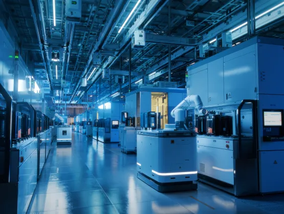
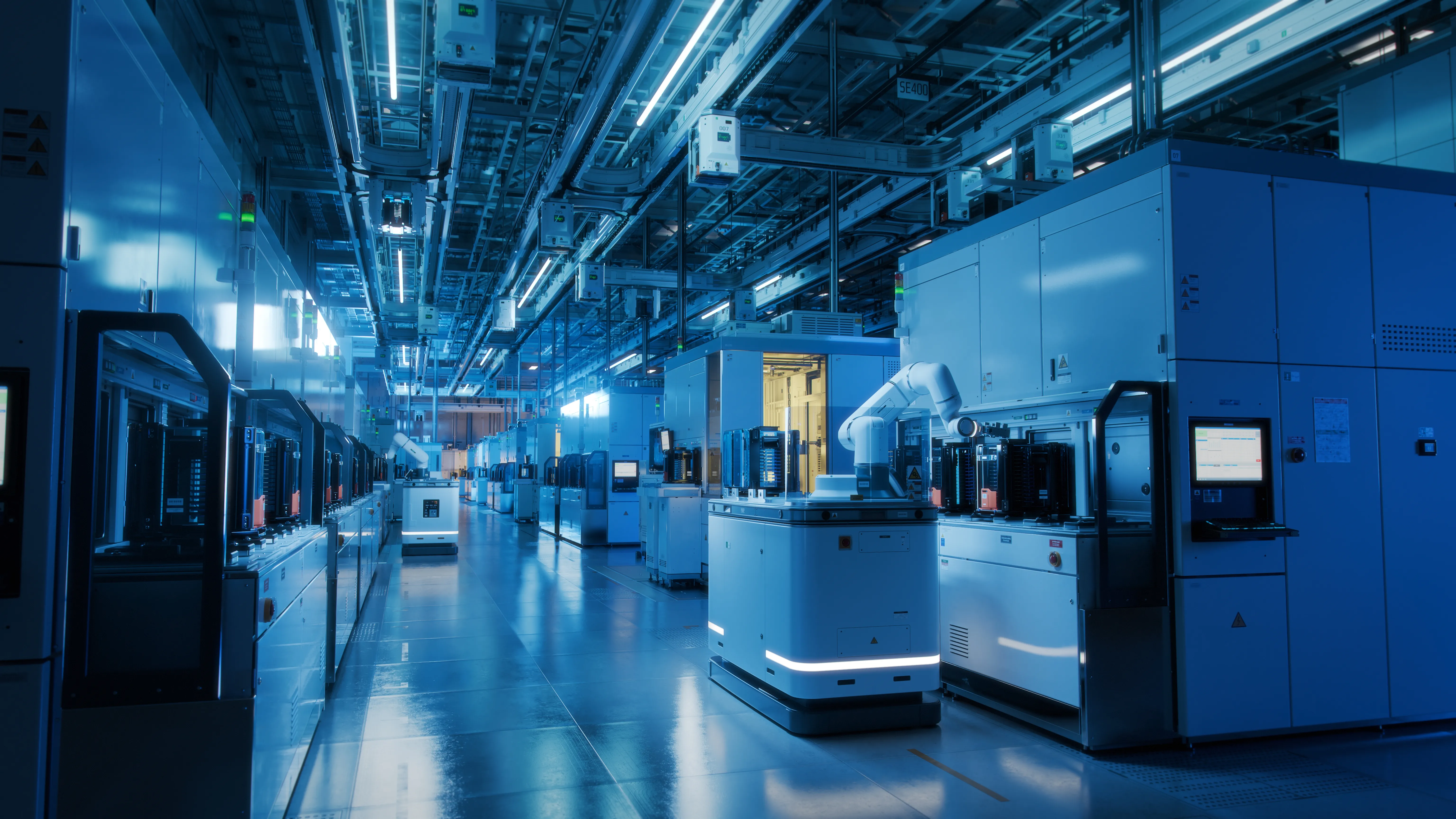
Advanced packaging is no longer operating behind the scenes. The technology of advanced packaging is helping to sustain the speed of the semiconductor industry’s improvement in power and performance, even as the Moore’s Law roadmap for wafer-level scaling comes under strain.At the Advanced Packaging Conference during SEMICON Europa 2025 in Munich, global experts examined the growth trajectory of this critical sector and Europe’s potential to lead in next-generation packaging solutions.Market Momentum Fueled by AI and HPCRomain Fraux, Chief Research Officer at Yole Group, forecasted that global revenues for advanced packaging will grow from $46.1 billion in 2024 to $79.4 billion by 2030. “Everything is linked to AI and high-performance computing (HPC),” said Fraux, while also emphasizing the growing relevance of automotive applications in driving demand.Romain Fraux, Chief Research Officer, Yole GroupThis demand is accelerating innovation across the supply chain. One emerging area is panel-level packaging, which breaks away from traditional round wafers. As Andreas Wocko, Sales Manager at Lam Research, observed, “Since the 1970s, the semiconductor industry has built on wafers. Now we are not just scaling, we are reshaping, building in a square format for the first time” – an innovation which substantially increases area efficiency and reduces device cost. Andreas Wocko, Sales Manager Europe, Lam ResearchTechnology Transformation from Lab to FabEurope is already investing in the foundational technologies that will power tomorrow’s packaging systems. Rolf Aschenbrenner, Deputy Director of Fraunhofer IZM, the home of the European Union’s APECS advanced packaging pilot line, discussed ongoing research into functional interposers, routing density, and organic interposers. “Our goal is to show how a new design philosophy incorporating chiplets can be brought to the industrial systems level,” said Aschenbrenner.Rolf Aschenbrenner, Director Deputy, Fraunhofer IZMThese breakthroughs are essential, as pitch sizes shrink and new materials emerge. Dr. Jessica Stubbe, Global Application Manager at MKS Atotech, described how interconnect densities have doubled in the past two years, with the industry moving to pitch sizes of less than 10µm. Stubbe said this new technology “will be enabled by a move from traditional solder-based interconnects to copper-to-copper hybrid bonding to provide higher density I/Os and lower resistance.” Jessica Stubbe, Global Application Manager, MKS AtotechInnovation Meets Real-World IntegrationThis increased density carries thermal risks with it. As Ram Trichur, Global Head of Semiconductor Packaging at Henkel Corporation, said, “New architectures enabled by advanced packaging are putting power devices on the backside, interposer or substrate, and this addition of more power delivery components in the package creates more local hotspots.”The reduced feature sizes inside the latest packages make it more difficult than ever to apply thermal interface materials. “At Henkel, we are now making 1µm-level fillers which enable the effective filling of gaps as small as 7µm,” said Trichur.Ram Trichur, Global Head of Semiconductor Packaging Market Segment, Henkel CorporationOne of the applications which stands to gain the most from the development of advanced packaging technology is silicon photonics. Dr. Himani Kamineni, Director for Advanced Packaging at GlobalFoundries, described how co-packaged optics (CPO) brings photonics directly inside the package, reducing connection lengths from centimeters down to millimeters, and providing higher bandwidth and lower latency at lower power. “Advanced packaging and CPO are foundational elements for AI and data centers to enable scalability to the next generation of compute,” said Kamineni. “But it will need a lot of packaging innovation: silicon interposers, copper-to-copper interconnects, and fiber-attach units for precise alignment.” Himani Kamineni, Director, Advanced Packaging, GlobalFoundriesReliability and Test Under PressureIn the transition to new packaging technology, it is crucial that the industry does not lose sight of the reliability standards which have made semiconductors so valuable in sectors such as automotive and aerospace. Amar Mavinkurve, Director of Materials and Labs Package Innovation at NXP Semiconductors, warned the finer spacing and smaller feature sizes in the latest packages posed a problem for reliability and long-term performance. He said, “We are dealing now not just with one failure mechanism, but with multiple. So, the way that we are used to describing behavior in models will not necessarily hold in future. Even industry standards might not hold.”Discussing new technologies such as copper-to-copper interconnects, Mavinkurve pointed out that failure would not be due to a single event, but to processes such as electromigration, corrosion, and thermomechanical effects. To model reliability properly in future, he said, “we need to move from a physics of failure to a physics of degradation.” Amar Mavinkurve, Director Materials and Labs Package Innovation, CTO, NXP SemiconductorsFabio Pizza, Business Segment Manager at Advantest Europe focused on quality and failure. With geometry scaling toward 1nm, early identification of known-good dies is essential to optimize cost and test coverage. Pizza said that, while device manufacturers need to keep time-to-market and the cost of test under tight control, they are also trying to figure out how to increase test coverage. “In a modern GPU, even a 100 DPPM quality process leaves 20 million transistors untested,” he said. Fabio Pizza, Business Segment Manager, Advantest EuropeEurope’s Position in the Global EcosystemThe conference concluded with a panel discussion about the prospects for Europe in the global advanced packaging market. According to Yole’s Romain Fraux, there is a strong ecosystem in Europe: “Europe’s strengths include specialized packaging service providers in the photonics and power market segments, as well as many packaging equipment manufacturers,” said Fraux. This resonated with the instincts of NXP’s Amar Mavinkurve and Advantest’s Fabio Pizza. Mavinkurve said: “We should focus on what we are already good at doing. It will be challenging to compete with advanced packaging providers elsewhere for AI and HPC business.”Ram Trichur of Henkel, however, urged the industry in Europe, “Do not take your foot off the gas on advanced packaging. You cannot do the full stack here, but in a technology such as CPO, there is a lot of innovation in Europe, and there is scope to add the manufacturing of these devices on top of the research capabilities.”Chris Scanlan, Senior Vice President of Technology at Besi, raised the idea of shifting production toward Eastern Europe. But Trichur cautioned that talent and infrastructure remain limiting factors in that strategy. From left to right: Chris Scanlan, Senior Vice President Technology, Besi;Amar Mavinkurve, Director Materials and Labs Package Innovation, CTO, NXP Semiconductors; Fabio Pizza, Business Segment Manager, Advantest Europe; Rolf Aschenbrenner, Director Deputy, Fraunhofer IZM; Ram Trichur, Global Head of Semiconductor Packaging Market Segment, Henkel CorporationCollaboration is the Path ForwardSpeakers throughout the conference echoed a common message: advanced packaging is reshaping the semiconductor landscape, and global collaboration will be essential to success. “It is impossible for one country or one region to do the entire stack,” Trichur concluded. “Innovation must be matched with strategic partnerships to bring advanced packaging from research to real-world impact.”On behalf of SEMI, the SEMI Europe team would like to thank the industry leaders whose expertise and enthusiasm made this conference a resounding success. SEMI ContactCassandra Melvin, Senior Director of Business Development and OperationsEmail: [email protected]
Read More
In an era where performance and efficiency are essential, heterogeneous integration is rapidly becoming a foundational technology. The webinar “Heterogeneous Integration in Action: Powering the Next Era of Connectivity” featuring speakers from the HiCONNECTS project dives deep into the advances, challenges, and ecosystem-building necessary to bring next-generation integrated systems to life across Europe and beyond.HiCONNECTS (Heterogeneous Integration for Connectivity and Sustainability) brings together more than 60 partners across Europe under the Chips JU to explore how packaging, materials, architectures and software can be co-designed for industrial uptake.A Bold Ambition: Why This MattersConnectivity is the lifeblood of our digital age. From smart mobility and data centers to consumer electronics and factory automation, demands on performance, energy efficiency, miniaturization and flexibility keep growing.Heterogeneous integration offers a path to meet those demands by enabling dissimilar technologies, for example chips, sensors, RF, photonics, advanced packaging and AI accelerators to work together more seamlessly than ever before.Set against the backdrop of Europe’s broader ambitions under the EU Chips Act to strengthen its semiconductor ecosystem and technological leadership, projects like HiCONNECTS demonstrate how coordinated R D can translate into industrially relevant demonstrators and use cases.Key Themes from the WebinarBelow are some of the most compelling takeaways from the session:From Components to SystemsAcross all talks, one message was clear: heterogeneous integration is no longer just about better individual devices, it’s about system-level co-design.Speakers showed this in very concrete ways:In power device manufacturing, improving yield, process control and data correlation across the wafer line directly improves the reliability of integrated systems.In smart logistics and manufacturing, autonomous mobile robots combine LiDAR, cameras, 5G, on-board compute and collaborative AI to operate safely on factory floors.In life-science imaging, cryo-electron microscopes, AI-assisted screening and high-performance computing are tied together into a single workflow.In connected and autonomous mobility, radar, V2X modems, explainable AI software and human–machine interfaces form one integrated chain.You can no longer treat sensing, connectivity, compute and packaging in isolation – the value lies in how they are composed into complete systems.Ecosystem Consortium DynamicsTo realize heterogeneous integration, no single entity can go it alone. The webinar highlighted how large consortia such as HiCONNECTS bringing in universities, research institutes, packaging houses, system vendors, and tool suppliers are key. A strong theme: modularity and interfaces must be agreed upon early to allow parallel work across partners.Why Europe’s Timing is CriticalHiCONNECTS sits within a broader European push to strengthen the continent’s semiconductor capabilities and reduce systemic vulnerabilities in critical value chains. Europe already hosts strong players in photonics, packaging, system integration, robotics, automotive and research.What the webinar underscored is that coordination and shared infrastructure are now decisive:aligning manufacturing know-how with AI and data analytics,connecting application-driven demonstrators with underlying technology platforms, andensuring results can be replicated and scaled beyond a single lab or pilot line.Final ThoughtsThe “Heterogeneous Integration in Action” webinar was a timely, forward-looking snapshot of how Europe’s microelectronics ecosystem is moving from component-level innovation to system-level co-design, grounded in real industrial use cases.The journey is far from complete, but the payoff is clear: higher-performance systems, new classes of products in mobility, health and manufacturing, and a stronger, more resilient European position in semiconductors.Kartikey Srivastava, Manager, EU ProjectsSEMI Europe Phone: +49 151 1436 6324Email: [email protected]
Read More
The SEMICON West 2025 design program “The Convergence of Semiconductor Manufacturing and Design,” organized by the ESD Alliance (ESDA), a SEMI Technology Community, featured presentations about successful collaborations between the design and manufacturing markets. The three-hour program in a packed conference room included plenty of great material that we’re using as the basis for a blog series that you will see over the next several months. I’m working on them now based on my conversations with four of the speakers where we discuss key drivers behind the need for collaboration and what’s ahead.I’m starting with Dave Kelf, CEO of Breker Verification Systems, a company steeped in front-end chip verification, who describes an actual circular collaboration that effectively leverages AI and other electronic design automation (EDA) advances. We recently talked about collaboration, integrated design and manufacturing flows and AI.Smith: How does Breker define collaboration between design and manufacturing? Kelf: In general, at a technical level, we would define this collaboration as the sharing of data, methodology and/or information that improves both processes. As semiconductors become more complex, this sharing process is increasingly important to effectively manage the overall complexity of today’s chip designs.Smith: What trends are driving the need for this collaboration?Kelf: Apart from the ever-increasing size and density of semiconductors, there are specific trends that require more interaction between design, verification and manufacturing. Obvious developments include the advent of chiplets, given the changes in performance of signal paths, and 3D devices driving complex packaging, power dissipation and other issues. Design issues such as the increased need for SoC coherency testing and complex device structures such as multi-core processors, also play a role. With many of these issues, design and verification (D/V) trade-offs have an impact on manufacturing, and vice versa. For example, differing delays on a Universal Chiplet Interconnect Express (UCIe) interface—an open specification for a die-to-die interconnect and serial bus between chiplets—will have an impact on hazard testing in coherency verification. As another example, thermal hotspots on some parts of a chip package might need additional testing during the verification phase. Smith: What trends and challenges are preventing a fully integrated design and manufacturing design flow?Kelf: Traditionally, the D/V and manufacturing teams have remained separate in most organizations, as well as between the two industries. EDA companies sell primarily to the design teams, although they do interact with the foundries at the back end of the process. Manufacturing companies work directly with different teams at the foundries and not with the D/V teams at all. New relationships need to be built up. The general know-how in these disciplines is different, and methodology approaches tend to be disconnected. The tradition is to separate the processes and use standardized interfaces for communication that leaves little room for improvisation. All this needs to change so that teams can begin to work more closely.Smith: What is circular EDA-manufacturing collaboration and vertical integration?Kelf: In past EDA flows, we have seen disparate tools performing specific functions. As semiconductors got smaller, their physics changed and this led to the design process absorbing new characteristics. For example, abstract designs were run through synthesis to create gates connected by wires. This format was then passed to place and route (P R) tools that would lay out the gates in terms of transistors and interconnects on the silicon wafer. On large devices, the gate level signal delays were larger than the interconnect, allowing design to be separated from layout. As silicon became denser, the interconnect delays became the dominant factor, and the layout of the device impacted the design synthesis process. The two tools required forward integration—synthesis projected layout rules to P R, and a reverse integration where layout characteristics were sent back to synthesis for redesign where required delays could not be handled during P R. The methodology went from a simple flow to a circular design approach as synthesis and P R cooperated. The same is now true of design and manufacturing where solving the problems noted above requires this same circular cooperation. Smith: What will it take to have an integrated design and manufacturing flow?Kelf: A lot of cooperation between different groups. As we reach limits in areas such as signal integrity and thermal management that will squeeze silicon efficiency improvements, these methodology linkages will be required for continued progress and growth. The industry (both design and manufacturing) will be highly motivated to make this happen. Smith: From a personnel perspective, who (on both sides) are the typical touchpoints? Kelf: It will be the engineering staff from both the design side and manufacturing that work closely to develop technical solutions. Executive-level support is, of course, needed to cement the collaboration. Smith: Where does AI fit?Kelf: AI will have a role to play in this. Estimating the factors that drive efficient design to manufacturing to design flows is a critical step in speeding interaction and providing sensible estimated starting points. AI can process the large amounts of data necessary to provide these estimates as we now see complex chips that contain billions of transistors. AI will be needed to accelerate the interactions for different tools through the development process.As design and manufacturing collaboration becomes a critically important industry strategy, companies are turning to SEMI and its Technical Communities such as the ESDA and their wide-ranging initiatives. For details and to get involved, visit the ESDA website at https://www.semi.org/en/communities/esda. To learn more about Breker and its solutions that provide test content portability and reuse to solve complex semiconductor challenges across the functional verification process, go to: https://brekersystems.com.About Dave KelfDave Kelf holds the position of CEO of Breker Verification after serving as its Chief Marketing Officer responsible for all aspects of Breker’s marketing activities, strategic programs and channel management.Earlier, he served as vice president of worldwide marketing solutions at formal verification provider OneSpin Solutions, was president and CEO of Sigmatix, Inc., and held senior positions at Cadence, Synopsys and Springsoft. Kelf holds a Bachelor of Science degree in Electronic Computer Systems from the University of Salford and a Master of Science degree in Microelectronics from Brunel University, both in the U.K., and an MBA from Boston University.Robert (Bob) Smith is executive director of the ESD Alliance, a SEMI Technology Community. 
Read More
Silicon carbide (SiC) has become a cornerstone of next-generation power electronics, driving advancements in electric vehicles, renewable energy, and industrial applications. After several years of rapid capacity expansion, the SiC industry is now entering a new phase focused on optimization, quality, and long-term scalability.This transition reflects a broader realignment across the global semiconductor ecosystem. As new fabs come online and supply chains mature, the industry is prioritizing stability, cost efficiency, and technical excellence over sheer capacity growth. SiC has moved from being a niche technology to a critical enabler of the energy transition, and this maturity demands not only investment in tools and materials, but also in process knowledge, cross-industry standards, and long-term partnerships that can sustain innovation at scale.To understand how this shift is unfolding, SEMI Europe spoke with Dr. Mark Puttock, Senior Director, Technology and Innovation at Entegris. Puttock shared his perspective on the industry’s evolution and how strategic collaboration and process innovation are shaping the next chapter of SiC manufacturing.From Ramp-Up to RefinementThe early growth of SiC manufacturing was driven by surging demand for high-efficiency power devices, particularly in electric vehicles. According to Puttock, that expansion period has given way to a new focus on yield, uniformity, and process control.The industry is entering a stage of maturity where success depends on optimization rather than scale alone. Improving consistency across crystal growth, wafer, and device fabrication is becoming just as important as adding capacity. This refinement phase calls for closer integration between materials science and manufacturing technology to ensure reliability and cost efficiency.A Focus on Process and Materials InnovationAs SiC moves toward high-volume production, challenges related to contamination control, defectivity, and wafer uniformity are taking center stage. Puttock noted that addressing these issues requires collaboration between materials suppliers, equipment manufacturers, and device makers.Efforts across the industry are converging on similar goals: enhancing purity, improving process repeatability, and developing new methods to enable larger wafer formats. Moving from 6-inch to 8-inch SiC wafers, for example, is widely recognized as a key step toward higher throughput and cost efficiency. Puttock emphasized that innovation in materials science and manufacturing technology must go hand in hand to support this scaling trend.Insights from Cross-Industry CollaborationA recent Entegris blog post featuring insights from Volkswagen Group Components and Porsche Consulting explores how SiC adoption is reshaping manufacturing strategies beyond the semiconductor industry. The post also highlights the strategy paper developed by Porsche Consulting in collaboration with Entegris. This joint effort demonstrates the value of aligning semiconductor-grade precision with automotive manufacturing demands. By sharing perspectives across industries, partners can accelerate best-practice adoption and strengthen the overall ecosystem for wide-bandgap technologies.Building a Sustainable FutureSustainability remains an integral part of this optimization phase. SiC devices themselves enable energy efficiency in end applications, but the way they are manufactured is equally important. Optimizing material use, recycling process consumables, and improving chemical delivery efficiency all contribute to a smaller environmental footprint. As production scales, attention to both performance and sustainability will be key to long-term success.Looking ForwardThe transition from expansion to optimization marks a pivotal moment for SiC manufacturing. Industry focus is shifting from building capacity to mastering control, quality, and resource efficiency. Puttock sees the future of SiC as one shaped by deeper digital integration, data-driven process development, and continued collaboration across disciplines. These advancements will help enable more consistent, sustainable, and cost-effective production—laying the foundation for the next generation of high-performance power devices.At the same time, Entegris continues to invest in materials science, contamination control, and advanced process technologies that help its customers overcome the complex challenges of SiC manufacturing. By combining technical expertise with a collaborative approach, the company plays an active role in supporting the industry’s transition toward more efficient and sustainable production.James Lam is Business Development Manager at SEMI Europe.
Read More