downloadGroupGroupnoun_press release_995423_000000 copyGroupnoun_Feed_96767_000000Group 19noun_pictures_1817522_000000Member company iconResource item iconStore item iconGroup 19Group 19noun_Photo_2085192_000000 Copynoun_presentation_2096081_000000Group 19Group Copy 7noun_webinar_692730_000000Path
Skip to main content
Default Banner Image

Technology and Trends

The sensor revolution is shaping the future of connectivity, with innovation in MEMS and imaging technologies paving the way for a smarter and more integrated world.As the world becomes increasingly interconnected, MEMS and imaging sensor technologies are driving transformative changes across industries, shaping the future of connectivity, intelligence, and sustainability. Powered by advances in miniaturization, AI integration, and sustainable design, MEMS and imaging technologies are enabling groundbreaking applications—from autonomous vehicles to wearable health devices—while addressing urgent global challenges like climate change and energy efficiency. At the MEMS Imaging Sensors Summit 2024, Laith Altimime, President of SEMI Europe, emphasized the pivotal role of MEMS and imaging technologies. Setting the stage for discussions on technological breakthroughs and market trends, Altimime remarked, “Sensors are at the heart of the next wave of innovation, enabling unprecedented levels of intelligence that are transforming industries and fostering a smarter, more sustainable, and seamlessly connected future.”Laith Altimime, President, SEMI EuropeStefan Finkbeiner, CEO of Bosch Sensortec, underscored in his opening keynote how advanced sensor technologies are enabling life-changing use cases. “Sensors are all around us, though we don’t always notice them,” emphasizing sensors’ ubiquitous role in smartphones, wearables, and hearables. Finkbeiner highlighted miniaturization as a key challenge, noting that even as sensors continue to shrink, they are increasingly integrated with edge AI to enable efficient, local decision-making.Stefan Finkbeiner, CEO, Bosch SensortecSimone Ferri, APMS Group Vice-President and MEMS Sub-Group General Manager at STMicroelectronics, highlighted the pivotal role of sensors as a bridge between the physical and digital world, noting “the most sophisticated machine is the human – so it is best to emulate human capabilities to enable the next generation of devices to accurately measure the parameters of your body.” Ferri stressed the importance of sustainability, advocating for smart, transformative, and precise sensors that provide meaningful data with optimal efficiency. By aligning technological innovation with environmental responsibility, Simone Ferri demonstrated how sensorization can enhance lives while enabling a net-zero transition across industries.Simone Ferri, APMS Group Vice-President and MEMS Sub-Group General Manager, STMicroelectronicsMEMS Growth Fueled by Piezo Materials and ElectrificationJean-Christophe Eloy, CEO and President of Yole Group, grounded the discussion in market data, forecasting a 5% CAGR for the MEMS market, which is set to exceed $20 billion by 2029. He highlighted key trends such as the increasing sophistication of automotive sensors—more cameras, higher resolution—and the impact of electrification. On the technology front, Eloy noted a “strong shift towards piezoelectric (piezo) MEMS,” driven by advancement in new materials like Lead Zirconate Titanate (PZT), Aluminum Nitride (AIN), and Scandium-doped Aluminum Nitride (ScAIN).Jean-Christophe Eloy, CEO and President, Yole GroupAlissa Fitzgerald, CEO of A.M. Fitzgerald Associates explored the expanding roles of MEMS technology in new domains, such as fiber optics for data centers. “Photonics is in the news,” she remarked, highlighting its potential to deliver 40% power savings compared to copper technologies. “MEMS manufacturing is set to evolve by 2030 and beyond,” said Fitzgerald, emphasizing the continued innovation in traditional wafer-based processes through the adoption of advanced thin-film materials like piezoelectrics and GaN. Furthermore, Fitzgerald discussed emerging manufacturing techniques such as 3D-printed MEMS and biodegradable materials to enable low-cost, sustainable sensors.Alissa Fitzgerald, CEO of A.M. Fitzgerald AssociatesAdding to the conversation on manufacturing, Jessica Gomez, CEO of Rogue Valley Microdevices, shared her perspective on how 300mm-capable MEMS foundries could “change the game,” improving production efficiency and lowering costs. Gomez also outlined the unique challenges of MEMS manufacturing, including the need for custom processes and the high-mix, low-volume nature of production.Advancing Smart Mobility Through Interoperable NetworksSmart mobility gained significant traction as Patrice Ancel, In-Vehicle Technologies Leader at BMW, tackled the intricacies of in-vehicle networking. Ancel shed light on the complexities of today’s vehicles, which contain 20,000 components and over 100 electronic control units (ECUs) from multiple suppliers. His message was clear: “Interoperability is key for us; without interoperability, none of this will happen.” Ancel’s call for collaboration resonated throughout the summit, highlighting the critical role of teamwork in driving innovation and progress within the automotive industry.Patrice Ancel, In-Vehicle Technologies Leader, BMWA Vision for the Future: Sustainability, Collaboration, and InnovationThe MEMS Imaging Sensors Summit demonstrated how collaboration, sustainability, and innovation are driving the sensor industry forward. From addressing market trends to tackling manufacturing challenges, the discussions revealed a shared commitment to creating a smarter, more connected world.On behalf of SEMI, the SEMI Europe team would like to thank the industry leaders whose expertise and enthusiasm made this summit a resounding success. SEMI ContactAna Bernardo, Manager of Technology ProgramsEmail: [email protected] Mobile: +49 175 4129 764Sitong He, Communications Manager Email: [email protected]: +49 151 5546 2638
Read More
Integrated photonics offers the semiconductor industry a new way to increase the speed and capability of classical compute functions, as well as enabling quantum computing. The III-V Summit, hosted by SEMI Europe in partnership with Photon Delta at SEMICON Europa, opened with a compelling question: why is a photonics summit taking place in the middle of a semiconductor event? Ajit Manocha, President and CEO of SEMI, highlighted the growing convergence of the semiconductor and photonics industries, stating, “It is my firm belief that a boost to Moore’s Law will come from the III-V world.” Declaring that the rate of growth in integrated photonics is set to pick up substantially, Manocha assured, “I will be your ambassador to make sure that the III-V technologies gain far greater visibility than they have today.”Ajit Manocha, President and CEO, SEMIThe promise of new III-V technologies is generating significant excitement within the semiconductor industry. Abdul Rahim, Ecosystem Manager at PhotonWorld, acknowledged the reality that today’s III-V device industry operates in a limited sphere, stating, “The III-V world is still at the interface of industry and academia. There is one main application for III-V devices – transceivers for data centers.” Abdul Rahim, Ecosystem Manager, PhotonWorld Carlos Lee, Director General of the European Photonics Industry Consortium (EPIC), echoed this message, “Photonics is not so much an industry today; it’s an ecosystem. It lacks the standards, roadmaps, and market data that a full-fledged industry needs – but we are getting there.” Carlos Lee, Director General, European Photonics Industry Consortium (EPIC)However, Rahim pointed to a number of trends that are driving the growth of III-V technology for integrated photonics. One key development is large-scale integration, “over the years, the number of devices in one photonics integrated chip (PIC) has been growing fast, reaching tens of thousands of components on-chip,” Rahim explained. Additionally, the widening frequency range supported by III-V devices is unlocking new applications beyond the telecom sector. Broad Scope of Research into III-V Technology for Integrated PhotonicsResearch into III-V technology spans an impressive range of materials, processes and applications. Nick Singh, CTO at Compound Semiconductor Applications (CSA) Catapult, a government-backed technology incubator, described in detail the most important fields of research that are driving innovation in integrated photonics. “III-V materials are special because they can be engineered,” Singh explained. Highlighting their potential role in advancing quantum computing, Singh added, “The ability to use new materials is crucial to reducing the reliance on algorithmic compensation for errors and non-linearity in hardware.” Nick Singh, CTO, Compound Semiconductor Applications Catapult However, Singh emphasized the need for the photonics industry to address structural challenges that could hinder progress. “Collaboration is crucial to standardize process development kits (PDKs) for photonics device fabrication processes—it’s like the Wild West in PDKs right now,” Singh remarked. “Additionally, the availability of raw materials presents a significant challenge.”The truth of this warning was confirmed by Diane Scott, Vice President of TECHCET, stating, "The US has deemed gallium to be the number one supply chain risk among a list of 50 raw materials, and the European Union (EU) has identified gallium as a critical raw material."Diane Scott, Vice President, TECHCETSuch geopolitical concerns have done little to dampen the intensity of research in III-V technology. One of the powerhouses of integrated photonics research is IBM, and Heike Riel, a Fellow at IBM Research with a special interest in quantum computing, revealed promising avenues that IBM is exploring. “IBM has developed local III-V-on-silicon heteroepitaxy, “Riel explained. “Using a direct growth method, we can grow vertical, lateral, and even 3D structures in III-V, such as stacked GaAs structures.” Riel highlighted the potential applications of this technology in emerging processor designs, including the Artificial Intelligence Unit (AIU) and analog computing devices with in-memory logic. “Here, we can deploy GaAs as a photorefractive material, used as a grating, to perform the same function as conventional electronic non-volatile memory in an analog computer chip,” Riel noted. Heike Riel, IBM Fellow, IBM ResearchAlso at the forefront of photonics integration is Black Semiconductor, a start-up company based in Aachen, Germany, which is developing devices using graphene. Cedric Huyghebaert, CTO of Black Semiconductor, shared the company’s vision, “We want to use electronics to compute, and photonics to transfer data, and bring both functions together on the same chip.” Black Semiconductor’s mission is to become the first foundry to offer integrated graphene technology. “Our ambition is to integrate graphene in line with semiconductor standards using semiconductor tools – avoiding the need for exotic processing technologies,” Huyghebaert explained. “We also aim to demonstrate co-integrated photonics on a 300mm wafer system, regardless of the process node. In doing so, we want to prove that deep technological innovation of this kind is possible in Europe.”Cedric Huyghebaert, CTO, Black Semiconductor GmbH Bringing Integrated Photonics to the MassesAs III-V technology develops to enable a broader range of integrated photonics applications beyond the telecom market, experts are recognizing the need for it to become more accessible if it is to be adopted by a wider range of manufacturers. Joni Mellin, manager of the photonics business line at the X-Fab Group, emphasized, “As an industry, we need to bring electronics design automation (EDA) tools up to a level of capability that matches that of the silicon world, so that you do not need a PhD to do product design – we need to make it accessible to ordinary electronics engineers.” Joni Mellin, BL Manager Photonics, X-FAB GroupAdoption of the technology also requires access to production capacity. Peter Maat, Senior Product Manager at SMART Photonics, an open foundry for indium phosphide (InP) programmable interface controllers (PICs), highlighted the challenges in this area. Maat explained that the availability of the foundry as “not a trivial capability,” because many InP fabs are run by integrated device manufacturers, and are closed to other users. The SMART Photonics business model aims to provide a comprehensive enablement service for fabless manufacturing of PICs. “Our responsibility is to produce stable, manufacturable building blocks that we make available to designers and to provide a platform which enables our circuit building blocks to be combined into an integrated photonics circuit,” Maat said.Peter Maat, Senior Product Manager, SMART Photonics Jayakrishnan Chandrappan, Head of Advanced Packaging Technology at CSA Catapult, also emphasized the importance of access to production capability. “The CSA Catapult has one of the world’s only sub-10micron hybridization facilities for advanced packaging that is open to third-party users,” Chandrappan noted.Jayakrishnan Chandrappan, Head of Technology, Head of Technology - Advanced Packaging, Compound Semiconductor Applications CatapultPromising Future for Integrated PhotonicsAs the summit concluded, the atmosphere was charged with optimism about the future of integrated photonics. The discussions highlighted how III-V materials, combined with advanced packaging, are set to play a pivotal role in shaping next generation technologies. A recurring theme throughout the event was the profound impact III-V materials will have, as they poised to become a corner stone of virtually every emerging technological advancement. SEMI ContactLaith Altimime, President of SEMI EuropeEmail: [email protected]
Read More
How Cool is That - Northrop Grumman’s “World’s Fastest Microchip” won the 2024 “Coolest Thing Made in California” contest, organized by the California Manufacturers Technology Association (CMTA). Public votes were cast for 138 California-made products in four rounds, culminating in this microchip—boasting speeds up to 1 terahertz—being crowned the winner. Manufactured in Redondo Beach, CA, the chip is 1,000 times faster than smartphone processors and represents California’s cutting-edge manufacturing sector. The contest and award ceremony were celebrated during CMTA’s MakingCA Conference, honoring manufacturing’s $310 billion contribution to the state’s economy. Doing the Green Wave - NIST scientists have successfully created a compact, full-spectrum laser covering the green-yellow-orange wavelengths, long considered challenging to produce. Traditional semiconductor lasers struggled with green wavelengths due to material limitations, so NIST turned to nonlinear optics, producing different wavelengths by adjusting silicon nitride device geometry and laser input. This breakthrough enables more precise, pure wavelengths ideal for quantum computing, medical devices, and underwater communications. Their method combines pump laser tuning and device adjustments, achieving 150+ wavelengths, demonstrating a significant advancement in accessible, high-quality lasers.Source: NIST’s Compact Green Semiconductor Laser - IEEE SpectrumEnergy Hero - At the 2024 ITF World conference, AMD CEO Lisa Su spotlighted a new goal: a 100x boost in computing efficiency by 2027. As shrinking transistor sizes yield diminishing returns, materials innovation has become essential for boosting performance and efficiency. Applied Materials has responded with advanced materials engineering solutions, harnessing exotic elements and 3D chip designs to improve efficiency. For instance, Applied’s Integrated Materials Solution™ combines six process technologies to reduce chip wiring resistance by 25%, a critical advance as semiconductor nodes shrink to the atomic scale. These methods promise breakthroughs in power efficiency across AI, personal electronics, and more. Building Automation of the Future - Imagine a future where every device in newly built structures— from HVAC systems and appliances to light switches and sensors—is equipped with a microprocessor and linked through a reliable communication network. This could transform how buildings operate, yielding substantial benefits across various sectors. Chip manufacturers would see new growth opportunities, while builders could offer smarter, more efficient homes. Consumers would gain convenience and comfort, as buildings could dynamically adjust to personal preferences and real-time needs. For instance, rooms would automatically adapt their temperature as people move through them, making manual thermostat adjustments obsolete. This automated approach wouldn’t just create a more comfortable environment but would also optimize energy use, potentially lowering costs and benefiting the environment.Source: Building Automation of the Future - EE TimesDo you have a fun fact to share? We invite SEMI members to share fun facts about the industry or their company. We’ll consider your tidbits for inclusion in future blog articles and or posting on social media. Complete our survey form or email [email protected]. Learn more about the SEMI Foundation and its initiatives to promote industry awareness and help provide a path for those interested in rewarding careers in microelectronics. Follow the SEMI Foundation on LinkedIn, Instagram, X and Facebook. Margaret Kindling is Senior Program Manager for Diversity, Equity, and Inclusion at the SEMI Foundation. She promotes inclusion and belonging via Women in Semiconductors, Semiconductor PRIDE and SEMICON West Workforce Development Pavilion programming.
Read More
With increasing demand for personalized smart devices, the MEMS and sensor market is undergoing rapid transformation. MEMS sensors are the backbone of smart wearable devices, seamlessly integrating multiple functions to monitor and simplify our day-to-day activities. As applications in healthcare, environmental tracking, and AR/VR expand, the need for ultra-compact, energy-efficient, and intelligent sensors is more critical than ever.In an exclusive conversation with SEMI, Stefan Finkbeiner, CEO of Bosch Sensortec, shared his perspective on the dynamic landscape of MEMS sensor technology. From Bosch’s evolution to a solutions provider with a focus on sustainability and market-driven innovations, Finkbeiner offered a deep dive into how Bosch Sensortec is positioning itself at the forefront of the industry. “We have to think in terms of the end application and determine what the right hardware and software configuration should be in order to provide solutions with the greatest benefit and flexibility.”Further insights into the future of MEMS and sensor technology will be shared by Finkbeiner during his keynote at the SEMI MEMS Imaging Sensors Summit on November 14, 2024, in Munich, Germany. Registration is still open.SEMI: Welcome, Stefan, and thank you for sharing your insights on advanced sensor technologies. Let’s start with a personal question: What motivates and inspires you about working in sensor technology?Finkbeiner: Sensor technology is very diverse and has significant impacts on consumers. We take pride in prioritizing consumers’ needs and benefits. True to the Bosch motto, “Invented for life,” we are committed to making life better, easier and healthier. This is demonstrated in our sensing solutions, which provide valuable data for fitness tracking in smartwatches, enhance the audio experience in hearables, and enable real-time monitoring of air quality to help individuals make informed decisions for a healthier environment. I am fascinated by technology advancements that are enabling the scaling of sensors—and the processing power and intelligence packed into these increasingly compact devices. For instance, our latest acceleration sensors for hearables are the smallest in the world and are nearly invisible at just 1.2 x 0.8 x 0.55 mm³.We leverage innovative wafer level chip scale packaging (WLCSP) to achieve this reduced form factor. These compact, feature-rich, high-performance accelerometers are easier to integrate in the latest generation consumer products where size and functionality are critical requirements.SEMI: How has Bosch Sensortec’s approach evolved over the years and what is the company’s primary focus today? Finkbeiner: We began our success story a few years ago as a hardware supplier, with one of our first applications being the 'Portrait-Landscape' function in smartphones. Over time, we’ve evolved into one of the leading providers of MEMS sensors.Today, we no longer see ourselves purely as a sensor manufacturer, but as a technology solutions provider. Our focus has shifted to think in terms of the end application and determine what the right hardware and software configuration should be to provide solutions with the greatest benefit and flexibility.Achieving this requires significant software and artificial intelligence (AI) development. In essence, we are optimizing software through self-learning models. Hardware remains essential for optimizing power consumption, with most sensors integrating a controller alongside the ASIC to enable seamless software integration.This unique software and hardware configuration unlocks exciting possibilities and broadens our market reach. We see significant growth in head-mounted devices, and we are actively working on related acoustics solutions.SEMI: Looking ahead, what trends do you anticipate will have the most significant impact on the MEMS sensors market?Finkbeiner: We see several trends that will significantly impact the MEMS sensor market. First, there is growing demand for personal health monitoring in consumer and mobile electronics. Wearable devices, in particular, are becoming essential tools for individuals to track their health and fitness status. This trend requires MEMS sensors to become even more accurate, with solutions that include sophisticated software algorithms to ensure reliability, accuracy, and reproducibility. As a result, AI and machine learning (ML) technologies will play a crucial role in enhancing sensor performance.A second important trend is the continued miniaturization of MEMS sensors. To meet customer demands, sensors must integrate more functionality, including edge-processing capabilities. For example, what once may have been a simple accelerometer with a step-counting algorithm is now evolving into a 6-axis Inertial Measurement Unit (IMU) with an integrated microcontroller and advanced AI/ML software. A great example of this is in True Wireless Stereo (TWS) earphones, where the IMU not only tracks steps but also enables complex tasks like dead reckoning and supports 3D audio—all within the tight constraints of a small TWS earbud housing. Low power consumption, as always, is a critical factor for these mobile devices to meet CE (Conformité Européenne) standards.Finally, we believe that smart glasses, augmented reality (AR) and virtual reality (VR) devices are poised to become the “next big thing.” These devices require advanced image projection optics that offer excellent optical quality, low weight, and ease of use to ensure consumer adoption. We believe our MEMS-based LBS (Laser Beam Scanning) solution is ideal for these applications. Additionally, the successful adoption of smart glasses hinges on high-performance MEMS sensors that are compact, accurate, and power-efficient—critical requirements for all-day wearability and functionality.These trends underscore the need for MEMS technology to evolve, integrating greater functionality, precision, and efficiency to meet the demands of next-generation consumer devices.SEMI: What are some of the biggest challenges facing the MEMS sensors industry today, and how can companies overcome them?Finkbeiner: One key challenge is that the smartphone market—arguably the most attractive market for a variety of MEMS and MOEMS sensors—has become more or less saturated. To stay competitive, MEMS companies must innovate existing products while also developing new, differentiated sensors and actuators for next-generation mobile products.SEMI: How is Bosch Sensortec supporting sustainability initiatives?Finkbeiner: We are helping to mitigate climate change with our low carbon footprint solutions.Up to 20% of annual global carbon emissions are caused by forest fires. This is equivalent to carbon dioxide emitted by all the vehicles driven worldwide. Our sensors can detect forest fires before they develop into wildfires by measuring various gases such as carbon monoxide and hydrogen. In parallel, we are working with our production partners to reduce our carbon footprint over the coming years, while also replacing or minimizing the use of environmentally hazardous chemicals, such as PFAS.SEMI: What are you most excited about for the MEMS Imaging Sensors Summit, and how do you think it will impact the European semiconductor industry?Finkbeiner: The European semiconductor industry has deep expertise in MEMS and sensor technologies, positioning it to make a significant impact in markets such as consumer health, optical sensing, and AR displays. By continuing to focus on sustainable solutions, we can drive even greater impact for the broader industry and secure Europe’s leadership in these growth sectors.I look forward to collaborating with industry peers at the Summit to define next steps needed to advance Europe’s leadership. The MEMS Summit is an invaluable opportunity to collaborate and drive progress, and I warmly invite my colleagues to join us in shaping the future of the European semiconductor industry.Dr. Stefan Finkbeiner Dr. Stefan Finkbeiner has been CEO and General Manager at Bosch Sensortec GmbH since 2012. He was born in 1966 in Freudenstadt, Germany. Stefan Finkbeiner held various senior positions at Bosch including Director of Sensor Marketing, Director of Corporate Research in microsystems technology, and Vice President of Sensor Engineering. He looks back on almost 30 years in semiconductor industry working in different positions related to sensor research, development, manufacturing, and marketing. Due to his wide experience in semiconductor and sensor industry, Stefan Finkbeiner is a recognized guest in panel discussions and as keynote speaker. SEMI ContactSitong He / Communications Manager, SEMI EuropeEmail: [email protected]: +49 151 5546 2638
Read More
In today’s rapidly evolving semiconductor industry, ensuring both precision and efficiency in manufacturing has become an increasing challenge, particularly as advanced technologies like MEMS and AI chips push the boundaries of design and production. Inspection methods that were once sufficient are now falling short, making room for cutting-edge solutions powered by artificial intelligence (AI). The introduction of AI-driven 3D X-ray inspection technologies is transforming the landscape, offering manufacturers a sophisticated tool to ensure quality control, while driving sustainable production strategies.SEMI spoke with, Joscha Malin, Product Manager, and Daniel Stickler, R D Expert for X-ray Imaging at Comet AG, Industrial X-Ray System Division, to explore how AI-powered 3D X-ray inspection technologies are shaping manufacturing. They delve into how these technologies address critical challenges during inspections and defect analysis, using tools such as Dragonfly 3D World software for user-friendly, AI-driven insights that facilitate effective decision-making.Further insights into the application of AI-powered 3D X-ray inspection technologies and their role in advancing MEMS manufacturing will be presented by Stickler at the SEMI MEMS Imaging Sensors Summit on November 14, 2024, in Munich, Germany. Registration is now open.SEMI: Thank you both for agreeing to share your insights. To start, can you explain the importance of inspection strategies in the context of MEMS manufacturing?Malin: As MEMS devices become increasingly miniaturized and complex, effective inspection strategies are crucial. These strategies not only accelerate the wrap-up of production processes, but also significantly enhance product yield. With tighter tolerances and various materials involved, ensuring the integrity and functionality of each component is more critical than ever. A robust inspection strategy allows us to catch potential defects early, which can save time and costs associated with rework or scrap.Stickler: The evolution of MEMS technology, particularly in AI chips, demands a higher level of inspection sophistication. Traditional methods may fall short in providing the necessary detail and speed, which is why we’re focusing on advanced solutions like our AI-powered 3D X-ray inspection.SEMI: Could you elaborate on how the 3D X-ray technology differs from conventional inspection methods? Stickler: The 3D X-ray technology we utilize acts as a bridge between traditional optical methods and standard 2D X-ray inspection. It offers high-resolution, three-dimensional images without damaging the samples. 3D X-ray technology emphasizes three main benefits: clarity, efficiency, and actionable insights. This means we can obtain detailed images that help us analyze components more effectively, allowing for real-time decision-making.Malin: Moreover, the clarity and detail provided by the 3D X-ray images are critical when it comes to defect analysis in MEMS devices. They allow us to assess mechanical, electrical, and assembly errors in ways that conventional methods simply cannot. This leads to a more reliable production process.SEMI: What specific MEMS defects can be effectively analyzed using this technology?Stickler: There are several types of defects we can analyze. For instance, we can detect mechanical defects such as stiction or fractures, as well as electrical failures like short circuits. The 3D X-ray inspection allows us to visualize these defects in detail. Additionally, we can monitor assembly errors, which are particularly important in complex MEMS devices where misalignments can lead to significant issues.Malin: I’d like to add that early detection of these defects is paramount. The faster we identify issues, the quicker we can implement corrective actions, thereby improving overall yield and reducing production costs.SEMI: You mentioned yield improvement earlier. Can you explain how your technology contributes to that?Malin: Our approach supports process optimization by providing information on product characteristics and, for example, allows us to identify trends early on that may lead to yield issues later. We also aim to accelerate new product introduction in the early phase by rapid feedback, saving time and cost. This is crucial because many defects may not be apparent until later stages of production. With our technology, we can monitor samples in real-time, allowing us to react promptly to emerging challenges.Stickler: By integrating this feedback loop, we can significantly shorten the time to market for new products. This is particularly beneficial in industries where speed and efficiency are essential.SEMI: Can you tell us about Dragonfly 3D World software and its role in this process?Malin: Dragonfly 3D World is a user-friendly software that leverages AI and, specifically, deep learning for image processing. It enables users to efficiently perform bump metrology and defect identification, for example, without needing extensive expertise in the field. The software makes complex processes manageable, even for operators who may not be specialists in image processing.Stickler: Beside MEMS and advanced packaging in GPU production, this software is indeed an “AI-for-AI” application. By utilizing deep learning, users can train models that adapt to various imaging tasks, making the entire inspection process more efficient. The insights generated from the 3D X-ray images are automated, enhancing usability and streamlining workflows.SEMI: In conclusion, what are the key takeaways you’d like to share?Malin: The key takeaways are that AI-driven 3D X-ray inspection is transformative for the MEMS manufacturing process, enhancing inspection strategies and defect detection significantly. By integrating advanced technologies, we can ensure higher product quality and efficiency.Stickler: Yes, and I would emphasize the importance of powerful monitoring and non-destructive test tools. Our innovative solutions not only improve yield, but also pave the way for sustainable practices in manufacturing, ultimately benefiting the industry. Dr. Daniel SticklerDirector X-ray Technology Components at Comet AG, Industrial X-Ray System Division. Based in Hamburg, Germany, he holds a PhD in Physics from the University of Hamburg and has extensive experience in X-ray imaging, semiconductor X-ray applications and product innovations. Joscha MalinDirector Product Marketing Software Products at Comet AG, Industrial X-Ray System Division. Based in Hamburg, Germany, he holds a degree in Electrical Engineering with specialization in Semiconductors and profound experience in the industry. For over a decade, he has focused on developing X-ray inspection and metrology solutions, especially for the Semiconductor industry. SEMI ContactSitong He / Communications Manager, SEMI EuropeEmail: [email protected]: +49 151 5546 2638
Read More
In the rapidly-evolving semiconductor industry, maintaining a competitive edge is crucial. To position Europe at the forefront of global semiconductor innovation, imec is leading the NanoIC pilot line initiative. Aligned with the European Chips Act, this initiative is a strategic move to bolster Europe's leadership in key markets like high performance computing, automotive, and healthcare.SEMI spoke with Srikanth Samavedam and Jo De Boeck from imec, Belgium, to learn more about the NanoIC pilot line and to better understand its goals, challenges, and prospects. From transitioning to gate-all-around (GAA) nanosheet devices, to developing advanced memory technologies and interconnects, this conversation highlights the cutting-edge advancements made possible through collaboration across the industry’s value chain.SEMI: How is the NanoIC pilot line working to revolutionize the semiconductor industry, and what are its main objectives?Samavedam: The NanoIC pilot line is a European initiative aimed at bridging the gap between R D and industrial innovation. The project is creating a beyond-2nm system-on-chip (SoC) pilot line, developing advanced logic, memory, and interconnect technologies. This effort supports the European Chips Act's vision for leadership and competitiveness in global semiconductor innovation, particularly in critical markets like high performance computing, communication, automotive, energy, and healthcare. However, advanced technologies come with more complexity, and addressing these complexity challenges requires more mature module baseline flows. By improving baseline flow repeatability and variability while reducing defectivity, we can accelerate the development of future technologies. The NanoIC pilot line is working to provide access to these advanced technologies and baselines to develop future compute systems. This will help ensure European competitiveness across the industry – from semiconductor materials, equipment and design to systems and applications.SEMI: Who are the core partners involved in this initiative?De Boeck: Key partners of the pilot line include CEA-Leti, Fraunhofer-Gesellschaft, VTT Technical Research Centre of Finland, Tyndall National Institute, and the Center for Surface Science and Nanotechnology of the University POLITEHNICA of Bucharest. This project is also supported by the Flemish government, other participating states, and the Chips Joint Undertaking of the EU Chips Act.These institutions and organizations bring a wealth of knowledge and resources, and imec compliments their efforts by providing access to its global partnerships with key industry leaders. The NanoIC pilot line is helping strengthen Europe’s global semiconductor industry leadership while aligning efforts with other regional Chips Acts. SEMI: Can you elaborate on the significance of transitioning from field-effect transistors (FinFETs) transistors to GAA nanosheet devices in CMOS technology?Samavedam: The transition from FinFETs to GAA nanosheet devices is a significant advancement in CMOS device technology. FinFETs have been the backbone of CMOS technology from the 22nm to the 3nm node. But starting at the 2nm node, nanosheet devices will need to be introduced. Nanosheet devices, including variants like Forksheet devices, are expected to drive scaling and performance through three generations – 2nm, A14, and A10. Complementary FET (CFET) architectures are also expected to be introduced around 2031 at the A7 node, which will represent another major inflection point in CMOS device design. This progression requires extensive research into new materials, process modules, equipment, and advanced patterning capabilities using high numerical aperture extreme ultraviolet (high NA EUV) lithography – all of which will be implemented on the NanoIC pilot line. FIGURE PROVIDED BY IMEC │ SCHEMATIC ILLUSTRATION OF A FUTURE COMPUTE SYSTEM. THE SYSTEM IS MADE OF LARGE MULTI-DIE ELECTRICAL-OPTICAL INTERPOSER PROVIDING ELECTRICAL AND OPTICAL INTERCONNECTS BETWEEN THE VARIOUS CHIPLETS (CPUS, GPUS, HBM). ALSO SHOWN ARE CONNECTIONS TO PACKAGE SUBSTRATE, AS WELL AS FIBER CONNECTORS AND AN INTEGRATED LASER SOURCE. CENTRAL PROCESSING UNIT (CPU); GRAPHICS PROCESSING UNIT (GPU); HIGH BANDWITH MEMORY (HBM); PROCESSING UNIT THAT CAN INCLUDE CPUS, GPUS, AND OTHER SPECIALIZED PROCESSORS (XPU); APPLICATION-SPECIFIC INTEGRATED CIRCUIT (ASIC); ELECTRONIC INTEGRATED CIRCUIT (EIC); FF-LEVEL: FEMTOFARAD-LEVEL; FIELD-PROGRAMMABLE GATE ARRAY (FGPA); GAAS QD: GALLIUM ARSENIDE QUANTUM DOT; INTEGRATED SILICON PHOTONICS PLATFORM 300MM (ISIPP300); REDISTRIBUTION LAYER (RDL); SILICON PHOTONICS (SIPHO); THROUGH PACKAGE VIA (TPV). SEMI: What are the key innovations necessary for advancing memory technology?Samavedam: As SRAM scaling slows, the exploration of novel, dense embedded memory concepts will become imperative. Technologies like spin orbit torque magnetic RAM (SOT-MRAM) and 2-transistor 0-capacitor (2T0C) embedded DRAM using deposited semiconductors like indium gallium zinc oxide (IGZO) are promising. These innovations address memory capacity and bandwidth challenges from new workloads in compute systems. Additionally, developing a 3D memory platform to explore future memory options will be essential for improving SRAM and DRAM. These advancements will help meet the demands of new applications like machine learning, augmented and virtual reality, and autonomous vehicles.SEMI: How do advanced interconnect technologies contribute to the future of semiconductor design?Samavedam: Advanced interconnect technologies, like chip-to-chip lateral (2.5D or interposer technologies) and vertical interconnects (3D technologies), play a crucial role in addressing memory capacity and bandwidth challenges. These technologies enable the partitioning of SoC functions into separate dies, allowing for more efficient and scalable designs. Advances like pitch scaling of micro-bumps and copper (Cu) hybrid bonding are facilitating this fine-grained partitioning of SoC functions. Additionally, optical interconnects and 3D interconnect-enabled co-packaging provide high-bandwidth and low-power connectivity at wafer scale. The rise of chiplet architectures and standardization will also increase the demand for low-cost, tight-pitch interconnect technologies like Cu/polymer redistribution layers.SEMI: How do your collaborators benefit from the NanoIC pilot line? De Boeck: One of the biggest collaborator benefits is the pilot line’s commitment to knowledge sharing through R D access and training. We invite foundries, IDMs, materials suppliers, equipment suppliers, and system companies/OEMs to jointly develop the materials, process modules, and integration flows to accelerate the development of beyond-2nm SoC technology pillars.Design pathfinding and system exploration process design kits (PDKs) will be available for start-ups, small- and medium enterprises, universities, and design and system companies to aid in prototyping and testing their designs. The NanoIC pilot line will also offer comprehensive training programs, including virtual PDK training, bootcamps for faculty, and internships and expert courses for students. To learn more, experts and key partners of the NanoIC pilot line will be presenting from 14 -16:40 at SEMICON Europa on November 12. imec’s program, ITF Chip into the Future, will highlight advancements in digital technology, capacity building through the European Chips Act, and the role of the NanoIC pilot line in accelerating beyond-2nm innovation. The conversation will also address industry requirements for pilot lines, emerging initiatives boosting Europe’s innovation and competitiveness, and perspectives on advanced materials and semiconductor equipment. Srikanth Samavedam, Senior Vice President of Semiconductor Technologies at imec, oversees programs in logic, memory, photonics, and 3D integration. Previously, he was a senior director at GlobalFoundries, leading 14nm FinFET technology into production and developing 7nm CMOS. Starting his career at Motorola, he worked on strained silicon and other advanced materials. He holds a Ph.D. in materials science and engineering from MIT and a master's degree from Purdue University. Jo De Boeck, Executive Vice President and Chief Strategy Officer at imec, oversees the company’s strategic direction and serves on its executive board. He joined imec in 1991 after earning his Ph.D. from KU Leuven and has since held various leadership roles, including head of imec’s Smart Systems and Energy Technology business unit and CTO. De Boeck is also a part-time professor at KU Leuven. Maria Daniela Perez / Communications Manager, SEMI EuropePhone: +49 160 2562977Email: [email protected]
Read More
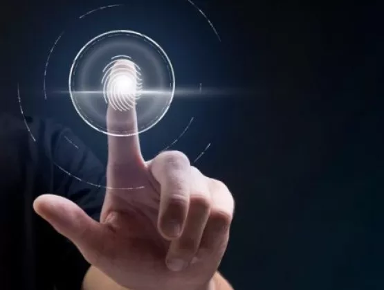
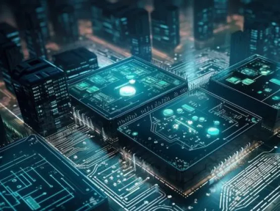
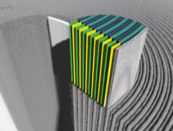
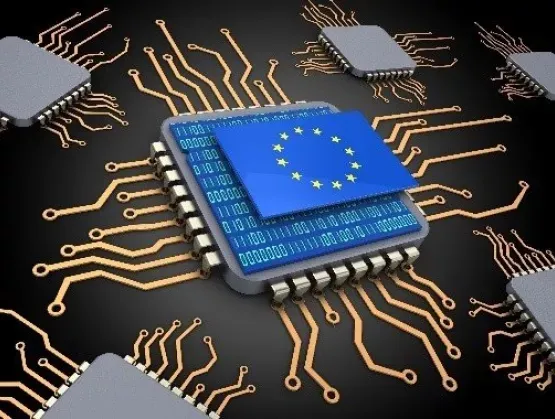
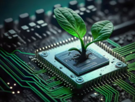
With the rapid proliferation of electronics applications with more powerful embedded intelligence, demand for smarter, more efficient sensors is increasing to help devices connect to the world around them. As the semiconductor industry drives the future of connected technologies and sustainable solutions, it faces challenges in energy consumption, resource management, and ensuring data security.SEMI spoke with Simone Ferri, Vice President and General Manager at STMicroelectronics (ST), about current trends and challenges in the Micro-electromechanical Systems (MEMS) and imaging sensors market and how ST is driving innovation in this rapidly evolving industry. Ferri shared insights ahead of his keynote presentation at the SEMI MEMS Imaging Sensors Summit on November 14, 2024, in Munich. Registration is open.SEMI: Welcome, Simone, and thank you for sharing your perspective on the dynamics and trends for today’s MEMS and imaging sensors. To start, how would you describe the current market dynamics for these technologies, and what key factors are influencing these dynamics? Ferri: Right now, the MEMS and imaging sensors market is primarily driven by applications such as automotive electronics, consumer medical devices, AI-powered devices, and intelligent wake-up systems.According to Omdia, the MEMS market is projected to reach approximately $11 billion by 2027, with a CAGR of 2.8% from 2022 and 2027. Currently, automotive applications account for 50% of this market, with industrial at 15% and consumer at 35%. Notably, the automotive sector is the fastest growing, with a 5.4% CAGR, driven by the increasing use of inertial measurement units (IMUs) and microphones.In addition, Yole Group estimates that the imaging market, including optical sensing, will grow at a 4.7% CAGR between 2023 and 2029. Although mobile phone applications remain the primary driver of Complementary Metal-Oxide-Semiconductor (CMOS) image sensors (CIS) volumes, other sectors, including consumer electronics, automotive, and security imaging, are also contributing to the growth.Long-term forecasts for smartphone sales have been trending downwards, but mobile phones still remain a major driver of applications, innovation, and overall volume in the imaging market. Notably, the automotive imaging sector is one of the fastest growing markets and is expected to drive additional demand for CIS.Factors that influence the current market include global economic conditions, regulatory changes, geopolitical factors, technological innovations, and the emergence of new applications and use cases.SEMI: Can you elaborate on the growth strategies that STMicroelectronics is adopting to stay competitive in the MEMS and imaging sensors market? Ferri: ST has played a pivotal role in both the MEMS and imaging sensors markets for over two decades with its proprietary silicon technologies. We fully leverage our Integrated Device Manufacturer (IDM) business model, which allows us to support our customers through integrated capabilities for both design and manufacturing.To remain competitive, we are exploring new markets for MEMS sensors, particularly in digital healthcare with biosensors, where wearable devices are expected to exceed 500 million units per year by 2027.We’re focusing on the growing demand for automotive sensors such as accelerometers, Inertial Measurement Units (IMU), and pressure sensors, particularly with the rise of electric vehicles. We are enhancing the integration and synergy between automotive and personal devices. For example, we are combining high-g and low-g accelerometers within a single IMU, enabling accurate fall and crash detection, along with precise orientation and wake-up functionality.AI is another one of our priorities. In today's digitalized world, AI enables real-time, contextual understanding and the ability to make decisions that optimize and reduce the power consumption of the final device. Sensors are no longer merely for data collection. Thanks to AI, sensors can interact with their environment and significantly contribute to innovation and sustainability.We are also prioritizing low power consumption. Our MEMS technology operates in low-power mode with almost negligible energy use, activating only when necessary, without waking up the system to understand its environment or to be reconfigured.In addition, we’ve seen optical sensing continue to grow year over year. Optical sensing now offers features such as 3D capture, low-power and low-footprint computer vision, Near InfraRed (NIR) and even Short Wavelength InfraRed (SWIR).We are accelerating and leveraging our IDM model and broadband semiconductor supplier positioning to propose wider system offerings based on the array of sensors and microprocessors that ST develops. As the world shifts toward widespread use of sensors and data collection, the demand for secure sensing technologies is growing, extending beyond mobile and PC applications to spatial computing and AR/VR environments. For example, if we are talking about recognizing specific persons in an AR environment, we don't want the data related to these persons to be sent to the cloud before a decision is made about whether they are supposed to be there or not, as such information can be intercepted. We want all the data to be managed at sensor level and only a warning of rejection or acceptance to be transferred outside our secure sensor. SEMI: What are some of the latest technological innovations in MEMS and imaging sensors that are shaping the industry? Ferri: In MEMS, we're seeing significant advancements in three key areas:- In-sensor AI is integrating technologies in the sensors such as machine learning core (MLC), adaptive self-configuration (ASC), and intelligent sensor processing units (ISPU).- Open sensors are designed to interface seamlessly with other sensors, allowing third parties to benefit from on-sensor processing innovations, while building an ecosystem to create joint value with customers.- Accurate sensors are providing high-precision data, enabling better decision-making and smoother, more natural user interactions. These sensors also reduce factory calibration time and resources, leading to overall lower energy consumption. Because of their accuracy, onboard MLC, and ASC, the sensors can also reconfigure themselves without interaction with the processor, thus guaranteeing the proper accuracy at lower power consumption, at any time, under any condition.In the imaging sensor market, key trends include:- Higher Pixel performance is leading to improved signal-to-noise ratio (SNR), low light performance, better quantum efficiency (QE) and lower noise performance. Despite post processing, pixel performance remains the key factor as SNR performance must remain high while the pixel shrink roadmap advances.- Embedded Intelligence is providing local processing for local decision making, enhanced security, advanced image sensor processing (ISP) for improved image quality, and fusing sensor functions to deliver a better user-experience.- "Always on" capabilities are supporting mass sensorization and deployment of optical sensing solutions everywhere through specific low-power design techniques, process development, and overall system architecture optimization.SEMI: Looking toward the future, what trends do you anticipate will have the most significant impact on the MEMS and imaging sensors market? Ferri: Some macrotrends for sensors include:Electrification: Certain consumer and industrial applications are now being adopted in the automotive sector, especially with the rise of electric vehicles creating new opportunities for innovation and for new players to enter the market. As example, the predictive maintenance that has been developed for industrial electric motors is ported 1:1 to electric vehicles.AI: Regarding data transmission, distributed architecture will push AI towards edge computing, increasingly supported by advancements in 6G and foldable technologies. Additionally, as AI becomes more integrated, the maintenance and security for AI will require more attention.Smart home, buildings, and cities: As cities grow, the demand for smart homes and buildings rises, requiring more sensors to manage energy, security, and urban infrastructure efficiently. Over 55% of the global population and 70% of the EU population reside in cities. Urban areas generate more than 80% of the world’s GDP, and by 2030, it's anticipated that 68% of the global population will be urban dwellers, pointing to the growing need for smart cities.Aging population and digital health: The integration of biosensors with MEMS technology will be crucial for addressing the needs of an aging population.Overall, the use of image sensors for environmental sensing is steadily increasing. This is a major focus for ST, particularly in 3D sensing. New use cases, such as presence detection, are enhancing security and reducing power consumption due to efficient data processing. Additionally, the average number of cameras in smartphones, automobiles, and even in devices like robots and vacuum cleaners, continues to grow.SEMI: What has STMicroelectronics been working on, and what are your plans for the upcoming years? Ferri: To date, we have shipped over 23 billion MEMS sensors. Still, we remain committed to continuously improving our products and enhancing our MEMS technology in terms of affordability, miniaturization, performance, and novelty. We are striving to set the stage for a future defined by innovation and excellence with:Evolution of our current product portfolio by investing in lower power consumption, lower supply voltage, and additional and more sophisticated in-sensor AI for an effective distributed AI conceptNew sensors for presence detection, like infrared (IR) sensors, and health-focused sensors such as biosensors.MEMS sensors are also becoming increasingly accurate, open towards different ecosystems of technologies, and so intelligent that they can self-configure and reduce power consumption thanks to optimal data processing. These attributes allow us to provide meaningful and sustainable solutions across sectors such as automotive, industrial, infrastructure, and personal electronics, enabling us to improve energy efficiency, reduce waste, and support sustainable practices for a greener planet.For the past 10 years, ST has focused on depth sensing across multiple use cases. Today, ST is the number one in the world for time-of-flight solutions through our ST FlightSense product family. More recently, we launched our global shutter image sensors family, ST BrightSense, to address markets like personal electronics, automotive, industrial, communications equipment, and computers and peripherals.More specifically on the automotive side, we have the portfolio, customers, and customer program awards to lead the driver and occupancy monitoring market. We continue to secure design wins from our growing customer base while we expand our product portfolio and broaden our customer and application footprints.SEMI: What are some of the biggest challenges facing the MEMS and imaging sensors industry today, and how is ST addressing them? Ferri: The MEMS and imaging sensors industry faces several challenges, but with strategic planning and innovative solutions, companies can overcome these obstacles by focusing on the following:Integration: With our biosensors, we are doing more with less space. For example, in a standard accelerometer, we integrate an analog front end for electrocardiogram (ECG) analysis, enhancing functionality without increasing the device footprint.Performance enhancement: Ensuring high performance and reliability in various environmental conditions is crucial, especially in automotive and healthcare applications. To meet these demands, we deploy comprehensive testing protocols to ensure our sensors meet performance and reliability standards.Power efficiency: Reducing power consumption is vital, particularly for battery-operated devices like smartphones and IoT devices. We are developing low-power architectures to address this need.Data security: With the growing use of imaging sensors in surveillance and personal devices, data security and privacy have become paramount. Our solutions include encryption for data transmission and storage, as well as robust access control mechanisms to prevent unauthorized access to sensor data.Additionally, supply chain issues remain a significant challenge today. We believe our strategy and capacity as an IDM, combined with our strong innovation capabilities, give us a competitive edge in supply chain management.SEMI: What are you most looking forward to at the MEMS Imaging Sensors Summit, and what does it mean for the European semiconductor industry? Ferri: I look forward to the Summit as a valuable opportunity to connect with industry peers, share insights, and explore new collaborations. I encourage my peers to attend, as it’s a unique platform to collectively shape the future of our industry and sustain Europe’s leadership in semiconductor innovation. About Simone FerriSimone Ferri is Vice President of APMS Group and General Manager for MEMS sub-group at STMicroelectronics. Ferri began his career in STMicroelectronics in 1999 as an R D engineer before becoming a digital designer for the company’s audio division, leading into product management after 5 years. In 2014, ST entrusted Ferri with MEMS consumer sensors followed by global MEMS-sensor related Marketing and Application activities across all markets and segments, leading into his current role. Ferri graduated with a degree in microelectronics from Politecnico di Milano (Polytechnic of Milan), where he also completed his MBA. Sitong He is Marketing and Communications Manager at SEMI Europe.
Read More
Verific Design Automation is an electronic design automation (EDA) developer of front-end software and a member of the Electronic System Design (ESD) Alliance. Verific is also viewed as a valued supplier to many EDA, field-programmable gate array (FPGA) and semiconductor companies –– some still around, some acquired by larger EDA companies, and some long gone –– for the past 25 years. With this backdrop, Bob Smith, executive director of the ESD Alliance, talks with Rob Dekker, Verific’s founder, president, and CTO, and Michiel Ligthart, its COO, about the evolution of the company and the industry over the last 25 years, the emerging EDA products space and what’s to come. Smith: This is the 25th anniversary of the founding of Verific. How did it get started? Dekker: The company I worked for before I started Verific was Exemplar Logic (now Siemens EDA), founded by Ewald Detjens in the 1990s. Exemplar started off making an RTL-to-Xilinx FPGAs path using the VHDL hardware description language (HDL) as the entry language. I worked on the VHDL language parser. As I was doing that work, I looked at the VHDL language reference manual and made sure that all the code complied with the rules set by the IEEE standards committee. I wondered why I was doing it for just one company, because it was and still is an IEEE standard language. Every tool vendor that wants to support VHDL would have someone like me looking at the language reference manual and building a language front-end that complies with all the rules in the standard. As I gained experience and finally left Exemplar, I already knew how to make a language front-end and started building a good one for the Verilog HDL. The initial idea was not to sell it to different companies but to build an equivalence checker formal verification tool that could be installed on every designer’s desktop, where they could check their designs at various stages in the design flow. I needed funding, and started selling the language front-end thinking that no one should have to rewrite a language front-end because it's already a standard. That's when the idea came to start Verific. I wanted to build a standard language front-end, with the possibility of creating a formal tool based on that front-end. The language front-end was popular among various EDA tool vendors and startup companies. Formal tools, synthesis tools, simulators or virtual prototyping tools, emulators, and so on all need a language front-end. I was starting to license the front-end and got so busy that I asked my good friend Michiel to run the business so I could focus on the technical side. After that, we started to grow, acquired an exceptional team in India run by my friend Abhijit Chakrabarty, and hired Rick Carlson as VP of sales. It quickly became a real company, and we started to license the language front-ends to the entire EDA industry. One company wanted to license our language front-end to build an equivalence checker. At that point, we had to decide whether to stay in the language front-end business or to make an equivalence checker and compete with our customers. We decided that competing was not a good idea and chose to focus on language front-end for the EDA industry. We have been doing this ever since for most EDA tools, from startup companies, all the way to large semiconductor companies. Their tools have been built with a language front-end developed at Verific, and we are proud of that. Smith: What have you seen change since you started? Have you seen any big changes that surprised you as the industry has evolved? Dekker: I wouldn't say big changes overall, but I've been impressed by the amount of innovation in the EDA industry. The industry is dynamic, with new tool vendors coming up and good ideas being explored. We are in a wonderful industry that is vibrant with innovation and talented people. This is what impressed me about the industry initially, and it still does. At Verific, we want to be an incubator for new innovations to flourish in an EDA industry dominated by a small number of large players. Ligthart: One change that had a significant impact on Verific specifically is the introduction of SystemVerilog. When Rob started out, there was Verilog 95 and VHDL. Verilog 95 was a relatively simple language. VHDL was complicated. We saw that early customers often wrote their own Verilog parser and came to Rob for the VHDL parser. In 2005, the IEEE 1800, also known as SystemVerilog, was introduced. That was a game changer, because suddenly, adopting SystemVerilog in the Verilog customer base required a new front-end that was as difficult to create as writing VHDL parsers. That was an inflection point for the company, and it started to grow. Before then, it was a nice company. After 2005, it became a growth company. Nowadays, we equally support SystemVerilog and VHDL. They're both complicated languages. People for the past 20 years have proclaimed the death of VHDL. It did not happen and will not happen. The two languages go hand in hand in different parts of the world. Most EDA companies support both because their end users require both. Smith: Verific coined the term “bespoke EDA.” How do you define it? Ligthart: For that, we need a bit of history. Fifty years ago, semiconductor companies started to write their own software tools to design their semiconductors. Those days, it was still called CAD, computer-aided design. Over time, we saw the introduction of EDA companies that tackled singular problems like simulation, place and route, or logic synthesis, and they started replacing in-house developed tools. In the past seven years, many of the larger semiconductor companies and system companies have started to develop in-house EDA tools again. Of course, they still license most of their design tools from EDA companies, but for certain design aspects, they develop their own design flow. They write their own internal EDA tools that are specific to that company, and they don’t go outside of that company. That's what we call “bespoke EDA.” Smith: These chip companies can afford to do this? Ligthart: Yes, because they are large enough and have the people to do it. They license their SystemVerilog and VHDL front-ends from us, so they do not have to invest five years of development for that piece of their flow. They take our parsers and elaborators and build something of their own — bespoke for their semiconductor design flow. Smith: It makes me think of Google, Meta. Ligthart: Let me put it this way. Of the magnificent seven technology stocks, six have a Verific license. Smith: How do you see AI changing EDA design tools? How will AI impact you? Dekker: This question about AI is coming up quite a bit, and I have a more conservative opinion. I don't know if AI is going to change EDA tools by themselves. EDA tools are highly optimized to do a particular task, it would be difficult for AI to beat that. If it did, it would surprise me. Outside of tools, like the design exploration phase for example, I think AI might make a humongous difference. AI could make it much quicker to explore different design alternatives. Right now, several AI-based companies are engaging with Verific, and they provide the design environment to do optimizations. AI could also help engineers improve their work. This would be more at the micro level, where individual engineers use ChatGPT type of engines and language models to enhance their programming styles, algorithms, and implementations. At the micro level, I think AI has an impact. At the macro level outside of the tools, I think AI will also have an impact. I doubt AI will change anything with the tools themselves. Ligthart: I'm pretty much in line with everything Rob said. At the Design Automation Conference (DAC), we showcased our relationship with four EDA startups that are applying or are in the process of applying artificial intelligence to their design objectives. As Rob said, the first step is getting a Verific license so that they have SystemVerilog already in place. Then, they apply AI-based algorithms to tackle certain aspects of the semiconductor design cycle. In terms of how successful they are, that's up to them to prove, but we have a front-row seat to watch their progression and success. Smith: What trends in the industry are you seeing? Dekker: Niels Bohr, a renowned physicist of the 20th century, once said, "prediction is very difficult, especially if it's about the future." Our EDA industry is vibrant, and it’s hard to see where it's going. I think that the EDA industry is here to stay. EDA companies are becoming more and more popular in the stock market. This industry is 40 years old, but it’s still dynamic and still full of innovation. It's extremely important that we keep this industry open, that we share ideas with each other, and that we provide solutions for the increasing complexity of chip and system designs, especially as AI gains prominence. The industry will change, and as it changes, the requirements for EDA tools will also need to be adjusted and there's a range of directions that our industry can go in. Verific is here to support that. About Rob Dekker Rob Dekker is president, founder, CTO and principal developer of Verific’s HDL source code software. Prior to founding Verific, Dekker was a software developer, manager, and director at Exemplar Logic, where he was the architect and a primary developer of Leonardo. Dekker started his career with Philips Research in the Netherlands, where he worked on the testability of VLSI circuits. He graduated from Delft University of Technology, the Netherlands, with a Master of Science degree in electrical engineering. About Michiel LigthartMichiel Ligthart is Verific’s COO and has an extensive background in engineering, product marketing, and general management. Prior to Verific, Ligthart was vice president and general manager of west coast operations for Theseus Logic, a startup in asynchronous logic. Previously, he spent eight years with Exemplar Logic in engineering and marketing roles. Ligthart started his career with Philips Research Labs and was a visiting scholar at the Center for Integrated Systems at Stanford University. He has a Master of Science degree in electrical engineering from Delft University of Technology, the Netherlands. Robert (Bob) Smith is executive director of the ESD Alliance, a SEMI Technology Community.
Read More
The drive to scale nodes towards physical limits, known as "More than Moore," and the adoption of 3D architecture in chip integration strategies for advanced logic and memory applications has led to unprecedented demand for high-quality dependable materials solutions. With the aid of digital solutions, the process is expedited with higher quality and efficiency.SEMI spoke with Thorsten vom Stein, Director, Head of Process Design Semiconductor Materials at Merck KGaA, Darmstadt, Germany, about how materials innovations and advanced packaging can contribute to smarter supply chain solutions for a sustainable ecosystem.More insights into key aspects of 3D architecture in chip integration and heterogeneous integration will be shared at the Advanced Packaging Conference (APC) during SEMICON Europa 2024, Nov. 12-15 in Munich, Germany. Registration is open.SEMI: What makes the digitalization of chemical process design for semiconductor materials manufacturing so challenging at a technology level? Vom Stein: The primary challenge in digitalization of process design is achieving data rich experimentation and design flexibility from the start. When we begin the process design for a novel material solution, the freedom of design needs to be very high for optimal outcomes. For example, to identify the best sequence of unit operations to achieve best process intensification, do we need a distillation or extraction after the reaction to meet the purity requirements? At the same time, the samples from these early process trials need to have purity levels and process reliability standards for high-volume manufacturing of routine production in order to meet the requirements of our customers’ leading-edge chip integration strategies. We address this need by executing data rich experimentation starting with first trial, and thereby establish “production ready” data density in the lab.To avoid confining our design space, we therefore need highly “sensorized” and automated modular lab equipment that can give us the data density we need and flexibility at the same time.SEMI: Are data-driven approaches also applied to streamline manufacturing processes? Vom Stein: Yes, data-driven approaches are key to driving cost, quality, process reliability and sustainable excellence. As we scale up from lab experiments to high-volume manufacturing—often times increasing volumes by two or three orders of magnitude—we scale the process model virtually ahead of its physical twin to de-risk these major scale-up steps. An example of this is simulating the effect of reactor geometry on the impurity profile.Establishing this handshake between the physical asset and the process model early in the development has a lot of benefits for sustained cost efficiency of the future manufacturing process. For instance, it allows for optimization of yield and cycle times to the existing asset infrastructure. Furthermore, we can achieve quality reliability critical to our customers by establishing end-to-end correlation models that link the quality of incoming raw materials to finished good impurity profiles.Finally, we can achieve the lowest possible carbon footprint and minimize waste streams and energy intensity via process intensification by matching the unit operation sequence to the specific thermodynamics and kinetics of the process.SEMI: How can advanced packaging contribute to the pursuit of net zero? Vom Stein: Ultimately in a successful process design, we aim to achieve the maximum yield of value-added product with minimal input of resources and raw materials. So, there is an intrinsic synergy between highly intensified processes and their carbon footprint. The digitalization of process design allows us to track the CO 2 footprint during every iteration of the design. Establishing this tracking as a routine design KPI is one of the key initiatives to drive net zero semiconductor material solutions.In addition, advanced process design is a key enabler for circular value streams. We are currently working on multiple projects to recycle waste streams and re-feed them as raw materials in our processes. We are also exploring how our chemical process technology can aid our customers’ recycling efforts such as reusing lithography cleaning solvent waste streams.SEMI: In your previous talks, you emphasized the importance of diversity, equity and inclusion (DE I). How is this related to the digital revolution? Vom Stein: In the not-so-distant past, my team consisted mainly of process chemists and engineers. Now, we are working with data scientists, model developers, automation experts and many more substance matter experts on our projects. This work requires an inclusive culture to maximize the impact of these diverse sets of insights and disciplines.We also must acknowledge that, in many instances, we are exploring unchartered territory that requires a “leap of faith” culture trusting in digital models. Imagine, for example, a production plant director who is used to a stepwise physical scale-up, now being onboard with skipping physical scale-up steps by using predictive process models. It takes time to really establish a trust in the “power of data.” This type of culture is championed at Merck KGaA, Darmstadt, Germany on all levels: from CEO to the production operator. Our DE I Report showcases how we continuously build belonging for over 64,000 employees across the globe.SEMI: Merck KGaA, Darmstadt, Germany is a key contributor to semiconductor innovations. How important is it for Merck KGaA, Darmstadt, Germany to collaborate with other industry leaders to achieve goals in matters such as sustainability and DE I? Vom Stein: Collaboration with our customers and OEM partners is a key piece of achieving the molecular precision necessary to drive technology evolution that serves as the backbone to society. More and more, we need to link our material solution manufacturing process to the process parameters of the tools in the fab, ultimately improving the chip yield of our customers. To transition from the nanometer era to the angstrom era, we must establish these process correlations end to end along the value chain, which is why we are heavily engaged on our Athinia collaboration framework.Besides technology enablement, sustainability is the next avenue where cross value chain collaboration is a must to lower the CO 2 and energy footprint of our industry. To this end, we have started a joint program with Intel on AI-enabled sustainable semiconductor processes.The importance of industry collaboration is why I was so honored to participate at SEMICON Europa together with representatives from leading companies.SEMI: What did enjoy about SEMICON Europa 2023 that you would like to experience again in 2024? Vom Stein: I was really impressed by the SEMICON Europa 20 Under 30 recognition program launched during the show. The program honored the brightest young leaders who have demonstrated success in their careers in the microelectronics supply chain. We were very happy with the acknowledgement of one of our brightest minds at Merck KGaA, Darmstadt, Germany, Balazs Bordas, Digital Twin Implementation Lead. He has been instrumental for many of our pioneering efforts in this space.Such recognition programs are very important for our industry and can make a significant difference in the perception of the semiconductor industry and its ability to motivate and attract more talent. I personally hope to see similar programs in the years to come.Additional resources:Learn more about diversity and inclusion at Merck KGaA, Darmstadt, Germany.Learn more about Merck’s KGaA, Darmstadt, Germany modular lab automation approach.Merck KGaA, Darmstadt, Germany sponsored SEMICON Europa and SEMI Advanced Packaging Conference in 2023. Thorsten vom Stein is Director, Head of Process Design Semiconductor Materials at Merck KGaA, Darmstadt, Germany. Based in Darmstadt, Germany, he holds a PhD in Chemistry from the RWTH Aachen University and has extensive experience in Catalysis, Materials Science, Process Development and Value Chain Innovation.Serena Brischetto is Director of Marketing and Digital Engagement at SEMI Europe.
Read More
In an era where technology permeates every aspect of our lives, the semiconductor industry serves as the backbone of innovation. From IoT devices to data centers, every piece of technology relies on integrated circuits (ICs) such as intellectual property (IP) cores and system on chips (SoCs). As these technologies become increasingly pervasive, the importance of hardware security assurance in the design and development of IP and SoCs cannot be overstated. Evolving cyber threats and sophisticated attacks make it essential for vendors to integrate advanced security measures into their workflows.Market Pressures Driving Demand for Enhanced Hardware Security The semiconductor market is projected to reach $1 trillion by 2030. At the same time, semiconductor devices and system designs are becoming increasingly complex. With that complexity comes the added difficulty and effort required to conduct thorough security analyses. Additionally, competitive pressure to reduce time-to-market means that vulnerabilities can be more easily overlooked or exploited, making it crucial for the industry to adopt automated security solutions. As more products are deployed in critical systems, from consumer electronics to national infrastructure, the stakes become even higher, underscoring the necessity for robust security measures.According to the SEMI Electronic Design Market Data (EDMD) report, in 2023, the electronic design automation (EDA), semiconductor IP, and related services market reached $17.1 billion, fueled by the increasing complexity of semiconductor designs and the growing emphasis on security. While the overall EDA market is growing at a 7.4% compound annual growth rate (CAGR), the semiconductor IP segment is expanding at 9.7%, and in comparison, the logic verification tools market alone is surging ahead at 24.2%. Deeper verification processes and tools are needed to not only handle the rising complexity of semiconductor designs, but also to support the growing emphasis on secure-by-design principles to ensure robust and reliable products in an evolving technological, security, and threat landscape. As a result, the market for logic verification tools — a key component of the EDA market — is surging. The Rising Cost of Cyber Threats from Data Breaches and Architectural Flaws Pavani Jella, Silicon AssuranceThe average cost of a data breach is $4.88 million1, encompassing lost business, regulatory fines, legal fees, and damage to brand reputation. As the semiconductor market grows, the potential financial impact of security breaches due to hardware vulnerabilities also escalates. Companies must invest in robust security measures to mitigate these risks and protect their financial health.Cyber threats from the exploitation of architectural flaws are another threat. Plundervolt is one example of an architectural flaw that could lead to hardware exploitation. Discovered by ethical hackers, Plundervolt is the name of an attack that exploited voltage fault injection to compromise the security of Intel processors. By manipulating the voltage supplied to the CPU cores, attackers could induce errors in the SGX enclave, allowing them to leak sensitive data or even bypass security protections intended by the enclave. This flaw was particularly concerning because it operated at the hardware level, making traditional software security measures ineffective. The attack leveraged the SoCs’ power management features, specifically dynamic voltage and frequency scaling (DVFS), to achieve its malicious objectives.Exploiting such a vulnerability could lead to the exposure of sensitive data, such as cryptographic keys and proprietary information, compromising the confidentiality of secure enclaves. This breach could erode trust in an IP or SoC provider’s security features, particularly in environments that rely on using the IP or SoC for protecting critical data. In cloud environments, a successful exploit could result in multi-tenant data breaches, impacting numerous users.The vulnerability also poses risks to secure applications, potentially leading to manipulated outcomes and decrypted communications. Businesses could face significant financial losses, operational disruptions, and regulatory consequences due to such an attack. It is a stark reminder of how architectural flaws in SoCs can be exploited, leading to severe security breaches that are challenging to mitigate without hardware-level fixes.Industry Believes Hardware Security Assurance Is a Key Priority A majority of security professionals from a diverse group across industry, defense, government, and academia rate hardware Trojan detection, IP piracy protection, and SoC vulnerability assessment as high priorities. This prioritization reflects the industry's awareness of the critical importance of security measures in maintaining the integrity and reliability of semiconductor products.As a result of this awareness, investments in cybersecurity are expected to reach $345.4 billion by 2026, growing at a CAGR of 9.7%2. This substantial investment demonstrates the global commitment to enhancing security measures across all industries, including semiconductors, to combat the escalating threat landscape.New EDA Tools and Investments Needed to Combat Cyber Threats The adoption of new EDA solutions is essential, despite the initial costs. Costs can range from $100,000 to $1 million per license for general EDA design and verification tools, depending on the complexity and capabilities of the software. Pre-silicon security EDA tools can detect vulnerabilities early in the design phase, significantly reducing the risk of exploitation and the need for costly post-production fixes while enhancing product reliability. Secure-by-design principles ensure that security measures are integrated throughout the development process, rather than added as afterthoughts.Integrating these new tools also requires investment in training and potential adjustments to existing workflows. However, the improved security and efficiency provided by these tools can offset these initial costs.While the costs of acquiring advanced EDA tools and deploying them in the workflow is significant, the investment is justified by the long-term benefits of enhanced security and reduced risk of costly breaches. Secure-by-design practices can prevent significant financial losses from security breaches, offering substantial long-term savings. Companies that invest in robust security measures are better positioned to demonstrate market leadership and build customer trust and loyalty, while avoiding the reputational and financial damage associated with breaches.ConclusionThe semiconductor industry is at a critical juncture where the application of advanced EDA solutions for hardware security is not just beneficial, but essential. The time to act is now.The increasing sophistication of cyber threats and the financial repercussions of security breaches make it imperative for IP and SoC vendors to adopt advanced EDA security assurance solutions to secure their designs. By investing in cutting-edge EDA tools and prioritizing security from the earliest stages of design, vendors can safeguard their products, maintain market competitiveness, and protect against the ever-evolving landscape of cyber threats.References1. IBM Cost of a Data Breach Report 20242. KPMG 2024 Global Semiconductor Industry OutlookPavani Jella is the Vice President of Business Development at Silicon Assurance, a member of the Electronic System Design Alliance (ESDA) a SEMI Technology Community. Silicon Assurance specializes in hardware security assurance solutions. With a strong background in the semiconductor and EDA industries, Pavani plays a pivotal role in driving strategic growth and fostering innovative partnerships. Passionate about the intersection of technology and security, she helps organizations adopt state-of-the-art solutions that ensure the resilience and trustworthiness of their hardware systems.
Read More