downloadGroupGroupnoun_press release_995423_000000 copyGroupnoun_Feed_96767_000000Group 19noun_pictures_1817522_000000Member company iconResource item iconStore item iconGroup 19Group 19noun_Photo_2085192_000000 Copynoun_presentation_2096081_000000Group 19Group Copy 7noun_webinar_692730_000000Path
Skip to main content
Default Banner Image

sensors

For nearly two decades, Sean Ding, CTO and chief scientist of Alibaba Cloud IoT, has worked in software and algorithm architectures, sensing, semiconductors, systems and cloud computing – all areas that have contributed to the rise of the Internet of Things (IoT). It’s no surprise, then, that Alibaba is leading next-generation innovation for the IoT. Ding will bring his expertise to his role as moderator of Brave New World - MSIG Conference on AI+IoT 2019, a half-day forum March 20, 2019, at SEMICON China in Shanghai, China. Maria Vetrano of SEMI spoke with Ding about technologies key to the IoT era including MEMS, sensors, artificial intelligence (AI), edge gateways and cloud computing. SEMI: MEMS sensors are widely used in IoT devices. What is the relationship between AI and MEMS sensors?DING: While MEMS sensors and AI will increasingly co-reside in end-user devices, I do not recommend adding AI next to the sensor (in the same package). That’s because designers continue to use the ASIC for signal conditioning, so A/D converters are still required. Rather, we should look to edge gateways to carry the majority of the workload, including deep learning, because this reduces system complexity and power consumption.SEMI: Why are smarter sensors shifting data processing and analytics to the edge of IoT devices?DING: Data processing and analytics are very important for IoT devices, but we need to focus on understanding the data, parameter calibration and more. The MEMS sensor industry should leave big data analytics to edge computing and cloud computing because AI requires deep learning, demanding a huge amount of data.The challenge is to find the sweet spot for data processing right next to the sensor element.SEMI: What is China’s evolving role in innovation in MEMS sensors for IoT devices?DING: At present, the MEMS community in China needs to figure out how to innovate instead of copying existing technologies, a low-margin business that will not help to grow the industry. One reason why I am so pleased to see the MSIG Conference on AI+IoT in China is that it will encourage greater creativity in the MEMS community in China, and this will ultimately lead to Chinese companies and R D institutions leading innovation rather than copying it.SEMI: What is the right approach to combining smart MEMS sensors with AI in IoT devices? Why is this important for both domestic Chinese and international markets?DING: Combining data from sensors with cloud-edge computing is the right approach. As sensor companies increasingly provide end-to-end solutions, such as “sensor+ firmware + SaaS + app,” we will realize easier and faster integration of sensors in IoT applications.This is incredibly important because China today is the world’s biggest market for IoT hardware. China has 2,000-plus design houses, 200-plus OEMs and thousands of distributors. That said, we still see a highly fragmented market that will benefit from a faster integration methodology.Faster integration of MEMS sensors and AI/machine learning for IoT hardware will benefit designers in international markets as well.SEMI: What do you hope MISG Conference on AI+IoT attendees will take away from the forum? DING: MEMS sensors are highly fragmented, reflecting the highly fragmented applications in which they play. The MEMS sensors industry should figure out how to provide one-stop-shopping solutions for vertical markets. This will speed the scalability of applications and expedite the growth of sensor production. Sean Ding (柯镇) will moderate Brave New World - MSIG Conference on AI+IoT 2019 at SEMICON China on Wednesday, March 20, 2019, at Kerry Hotel Pudong in Shanghai, China.This conference has been organized by the MEMS Sensors Industry Group (MSIG). Register today to connect with Sean Ding and featured speakers at the event.Speakers at the MSIG Conference on AI+IoT 2019 at SEMICON China include: Welcome and Introduction / 欢迎辞Carmelo Sansone, Director, MEMS Sensors Industry Group (MSIG), a SEMI technology community AI Needs Accurate Data – MEMS Sensors Can Provide It / MEMS传感器为人工智能提供真实数据Andrea Onetti, Group VP of Analog MEMS Group, GM of MEMS Sensor Division, STMicroelectronics Enhanced IoT Edge by Smart Sensors / 智能传感器助力IoT边缘智Bennini Fouad, Regional President Asia Pacific, Bosch Sensortec Horizon AI Processor Solution, Enable Industries in AI Time / 地平线AI芯片解决方案,赋能千万业Carl Zhang 张永谦, General Manager/VP, Smart Chip Solutions Division, Horizon Robotics Inertial Sensors in AI Applications / 运动传感器AI应用案例Ben Lee 李彬 , CEO, mCube Ultra-Low-Power Solutions: an Ecosystem Approach / 超低功耗的生态链解决方案Carlos Mazure, IEEE Fellow, Chairman Executive Director, SOI Industry Consortium High-Integrity, Fault-Tolerant Open Inertial Measurement Platform for AI-based Vehicle Automation / 适用于人工智能车辆自动控制的高集成及容错的惯性测量开放平台Dan Dempsey, Senior Director of Automotive, ACEINNA Maria Vetrano is a public relations consultant at SEMI.
Read More
At the SEMI FLEX 2019 and MEMS Sensors Technical Congress (MSTC) (MSTC) February 18-21 in Monterey, California, I had the pleasure of meeting many old friends and colleagues as well as making some great new acquaintances. With MEMS and sensors still a relatively young industry, I am delighted that our community is thriving. We continue to see double-digit growth rates, there is plenty of innovation, and the technology generates massive amounts of data that gets everyone excited about artificial intelligence, deep and machine learning, and blockchain. Those are all the buzzwords that any tech startup needs for funding these days.While it is hard to single out any one presentation at conferences, I was particularly struck by Nadia Shakoor’s keynote address, “Driving Advances in Crop Breeding and Smart Farm Management.” From Nadia I learned that the world’s largest agriculture sensing platform was a mere 45 minutes south of where I live in Phoenix, Arizona. This is a major embarrassment to admit as I have lived here for almost 30 years, have been involved in MEMS and sensors for a decade, and have a particular passion for the use of sensors in agriculture and food to improve crop yields and food quality, and to reduce food waste. This humongous sensor was hiding in plain sight right under my nose!After Nadia’s keynote, I just had to speak to her at the break. Nadia is the senior research scientist and project director for TERRA-REF at the Danforth Plant Science Center based in St. Louis, Missouri. Nadia’s work employs field-level crop phenomics, the biological study of the set of physical and biochemical traits belonging to a given organism (phenomes). Phenomes are fascinating because they change in response to genetic mutation and environmental influences. The Danforth Plant Science Center and its partners are involved in many phenotyping projects using autonomous vehicles, drones, field scanners, satellite imaging and more.After the FLEX MSTC event, I emailed Nadia to ask if I could visit the field scanner and her partner team at the University of Arizona in Maricopa, Arizona. She kindly introduced me to Maria Newcomb, a plant research scientist at the site, who gave me a good look at this mother of all field scanners: the Transportation Energy Resources from Renewable Agriculture Phenotyping Reference Platform (TERRA-REF). TERRA-REF aims to transform plant breeding by using remote sensing to quantify plant traits such as plant architecture, carbon uptake, tissue chemistry, water use and other features to predict the yield potential and stress resistance of 400+ diverse sorghum lines. The TERRA-REF Field Scanner at the University of Arizona Maricopa Agricultural Center. It’s the largest field crop analytics robot in the world, one that’s critical to the crop research underway at the Donald Danforth Plant Science Center in St. Louis, Missouri. Source: Steve Whalley TERRA-REF’s Lemnatec Field Scanalyzer is the largest field crop analytics robot in the world. This high-throughput phenotyping field-scanning robot has a 30-ton steel gantry that autonomously moves along two 200-meter steel rails that have recently been extended another 170 meters. It continuously images the crops growing below it by using a diverse array of cameras and sensors to observe the field at a dense-collection frequency with high resolution. These sensors include RGB stereo; thermal, chlorophyll fluorescence imaging system; hyperspectral cameras; a 3D laser scanner; and environmental monitors.Plant breeding is currently limited by the speed at which phenotypes can be measured, and the information that can be extracted from these measurements. Current instruments used to quantify plant traits do not scale to the thousands or tens of thousands of individual plants that need to be evaluated in a breeding program. The TERRA-REF field scanner system, on the other hand, uses sensors to scan over one acre of plants, collecting thousands of daily measurements throughout the growing season, and these are used to determine plant phenotypes and inform breeding decisions. TERRA-REF’s advanced sensor technologies include: Hyperspectral (250nm-2500nm) Thermal Infrared 2D and Stereo RGB PSII chlorophyll fluorescence 3D laser Environmental sensors The TERRA-REF field scanner platform features a massive sensor-rich scanner head. Source: Steve Whalley The humongous TERRA-REF field-scanner was certainly a sight to behold, looming like a cargo-ship container crane in the vast flat plains of the Arizona desert landscape. I’ve only scratched the surface of what this enormous sensor platform can accomplish so if you are a MEMS/sensor company interested in agriculture and food production, I encourage you to get more information at terraref.org and pay a visit next time you are in the area.Steve Whalley, CEO, Strategic World Ventures, is a strategic consultant to SEMI-MEMS Sensors Industry Group (MSIG). He also consults with established and emerging semiconductor, MEMS and sensors companies.
Read More
As group vice president of the Analog MEMS Group and general manager of the MEMS Sensor division at STMicroelectronics, Andrea Onetti brings nearly three decades of experience in MEMS, sensors and audio systems to his leadership role at one of the world’s most successful electronics and semiconductor manufacturers. During his keynote at FLEX and MEMS Sensors Technical Congress 2019, February 18-21 in Monterey, Calif., Onetti will address the criticality of sensor accuracy in advancing automotive, industrial and consumer applications. SEMI’s Maria Vetrano spoke with Onetti recently to give FLEX/MSTC attendees a preview of his presentation. SEMI: What are some promising advancements in sensors for autonomous cars? Onetti: The avionics industry is already successfully applying sensors for autonomous operationl. Inertial navigation systems (INS) support the operation of planes during flight, both after takeoff and before landing. Unfortunately, the technology in these navigation systems is expensive and not scalable, and they are hampered by reliability limitations in an automotive environment.Following the steady progress that we have made with MEMS inertial sensors in consumer applications, we are on the cusp of realizing greater accuracy in temperature and time – finally delivering the performance required for autonomous driving. Because we can scale in production – we’re now manufacturing more than a billion units a year – we can select the cream of this production crop for adoption in cars. Consequently, we should see Level 3 and Level 4 autonomous driving for consumers very soon.SEMI: How are companies using sensors to monitor and track their assets in industrial applications? Onetti: Predictive maintenance and asset tracking are the two main verticals in Smart Industry. The adoption of multiple sensors for condition monitoring is helping to detect the faulty operation of equipment and to detect early signs of issues that are otherwise difficult to capture. Ultrasonic microphones can detect leaks in a pipe at an early stage, accelerometers with high bandwidth can act as micrometers, and accurate temperature sensors can catch overheating. Similarly, in asset tracking, we use temperature monitoring in combination with inertial sensors to detect problems during the transport of goods. Shock sensors with extremely high full scale (up to 8000g) can tell whether a lightweight envelop has been dropped. Pressure sensors can switch off a radio system when a cargo plane takes off and can mute smart trackers in compliance with flight regulations. We really can do almost anything! A full slate of ST sensors and microcontroller units (MCUs) enable WEG’s small but powerful motor sensor, which listens to a motor, feels its pain, and shares that information with engineers, operators and others to diagnose problems before they happen. Image courtesy of STMicroelectronics. High-accuracy motion, environmental and proximity sensors are crucial to VR/AR. Image courtesy of STMicroelectronics. SEMI: How will sensors advance user experiences in consumer electronics, such as VR/AR systems?Onetti: Virtual reality (VR) and augmented reality (AR) are great examples of promising consumer technologies that will become pervasive as performance of inertial sensors improves. First, we need super accuracy in time and temperature to provide the right experience to users. To achieve this level of accuracy, we need a major step forward in performance, and that includes power consumption and miniaturization. Fortunately, we are constantly making progress in the high-accuracy motion, environmental and proximity sensors that are critical to these systems. While the scale is vastly different between VR/AR and automotive, the requirements for AR/VR systems are pretty similar to those that will enable autonomous cars. A growing variety of sensors (environmental, microphone, proximity, motion) – combined with a sensor hub in an MCU – are central to VR controllers (above) and VR head mounted displays (below). Images courtesy of STMicroelectronics. SEMI: We don’t hear much about the criticality of higher accuracy in sensors. Why is improving accuracy in sensors especially important – and what role do calibration routines play in achieving higher accuracy?Onetti: A sensor is more than just the performance of the relevant function. It is also the intrinsic accuracy that it brings. This accuracy is tuned by calibration, which is typically an expensive process done at the end of product manufacturing or – better still – during earlier stages of manufacturing.Today more applications require sensors with higher accuracy, which necessitates investing more time in calibration, leading to higher cost.MEMS technology can help by offering solutions with intrinsic higher accuracy, which reduces the cost of calibration for product manufacturers. This naturally delivers major benefits to OEMs and, ultimately, their customers.SEMI: What would you like FLEX and MSTC attendees to take away from your presentation?Onetti: As attendees explore the wide variety of available sensor solutions for their end products, I would ask them to prioritize the role of accuracy in sensor selection – because improved accuracy means higher quality data, and higher quality data means better decisions with reduced need for data processing.While designers understand the role of calibration routines in qualifying individual components for specific applications, it is the continuous evolution of MEMS technology that offers the best possibility of breakthrough reductions in time and cost of these calibration routines. This makes MEMS sensors more attractive and affordable than similar sensor components based on different technologies. Andrea Onetti will present Accuracy Enables MEMS Sensor Pervasion at FLEX/MSTC on Tuesday, February 19 at 11:00 am.Register today to connect with him at the event. To learn more about STMicroelectronics, click here. Maria Vetrano is a public relations consultant at SEMI.MSTC FLEX 2019 is organized by MEMS Sensors Industry Group (MSIG) and FlexTech.Maria Vetrano is a public relations consultant at SEMI.
Read More
Jason Jelinek, a software technical manager at John Deere Electronics Solutions, has parlayed his more than two decades of embedded software engineering experience into commercializing controls and sensing technologies for rugged/harsh environments, including agriculture/off-road and aerospace. During his keynote at the upcoming FLEX and MEMS Sensors Technical Congress 2019, February 18-21 in Monterey, Calif., Jelinek will address the driving need for advanced sensing technologies that will fuel the continued growth of autonomy in agriculture.SEMI’s Maria Vetrano asked Jelinek to help FLEX/MSTC attendees understand his vision of autonomy in agriculture, which heavily leverages advanced sensing technologies to help farmers master equipment logistics, handle vehicle- and fleet-level operational efficiency, and manage the entire lifecycle of crops.SEMI: Did autonomy in agriculture start with autonomous equipment, such as tractors and combines?JELINEK: Automation, the first step on the road to autonomy, has been occurring in agriculture for a long time. Over the past 100 years, automation has dramatically reduced manual effort and simplified jobs in farming, allowing operators to focus more on administrative and other aspects of their work.The evolution of the combine is a good example of automation in agriculture. Long ago farmers would use a scythe to cut down the crop before bundling or stacking it up. Later they would manually thresh and winnow the crop to get the grain. Over time, we developed windrowers to cut the grain, threshing machines to separate the grain from the chaff, and winnowing machines to get only the grain. Combines now “combine” all those steps to go from grain on the stalk in the field to grain in the hopper. One person in a combine can do the work that once required many people and animals — all in a much shorter timeframe. We are now looking at automating harvesting to maximize yield and reduce fuel consumption. The AUTOTRAC feature on John Deere machines is a recent example. AUTOTRAC divides a field into rows based upon the parameters of the machine in operation, supporting hands-free driving with very high accuracy. It allows consistent, accurate rows for tilling, planting, crop treatment and harvesting, saving considerable time, improving overall quality and freeing the operator to do other work while in the vehicle.The Exact Emerge and Section Control features (which also use AUTOTRAC) will spur greater future autonomy. Control over both the seed spacing (Exact Emerge) and when the machine drops seeds (Section Control) prevents overseeding and provides the right seed-spacing for optimal crop production.As we look to the future, sustained growth in automation of jobs will enable the development of fully autonomous equipment. Currently, however, skilled operators are still closely involved in job management and execution. To realize greater autonomy, we will need machines that make the decisions once made by people.SEMI: How will autonomy in agriculture change the ways that we grow and harvest food — and even affect when we sell it?JELINEK: Autonomy will lead to more efficient production, reducing fuel, fertilizer, herbicide and water requirements. It will also enable fewer people to do more of the work.Let’s start with conditions that are hard, even impossible, to control: weather and staffing.While farming is still tied to the weather — and will remain so for some time — more efficient operations will allow tilling, planting, spraying and harvesting of fields to occur in shorter time windows that more easily match conducive weather conditions.There is also a human-resource issue: The agricultural industry must compensate for population decline in the rural areas where farmers operate. Doing more with less is essential for agriculture to continue to meet the rising food and clothing demands of the world’s population.SEMI: To what degree will we see artificial intelligence in autonomous agricultural systems?JELINEK: While autonomous systems had their start at the vehicle level, they will one day move to the entire fleet, providing suggestions on when the owner should execute operations. Autonomous systems may also help owners to decide when to store or sell crops, based on market conditions, operating costs and desired margin levels. That’s the initial level of artificial intelligence that I foresee.SEMI: How can sensing improve autonomy in agriculture?JELINEK: The challenges we face in agriculture are many, but technology will help us meet them. We must transfer responsibility for operations and decision-making from the skilled operator to the intelligent machine. Through increased use of sensing, we can gather large amounts of data, which autonomous agricultural systems will process, communicate and interpret to streamline jobs and boost agricultural production.SEMI: What would you like FLEX/MSTC attendees to take away from your presentation?JELINEK: I would like FLEX/MSTC attendees to understand the environment in which agricultural sensors need to operate. We need sensing solutions that will survive and thrive in rugged, outdoor variable environments to support the automation that will fuel autonomy.I would also like to engage suppliers in the application of current technology to meet our sensing needs.Jason Jelinek will present Autonomy in Agriculture at FLEX/MSTC on Tuesday, February 19 at 9:00 am.Register today to connect with him at the event. To learn more, click here.MSTC Flex 2019 is organized by the MEMS Sensors Industry Group (MSIG) and FlexTech. Maria Vetrano is a public relations consultant at SEMI.
Read More
4 Key Takeaways from SEMI Taiwan Member ForumThe rapid development of artificial intelligence (AI) has accelerated the digital transformation in various industries and has now fused with Internet of Things (IoT) to exploit the value of both technologies in reshaping the electronics industry value chain. As it emerges from the shadows of its parent technologies, AIoT is giving rise to new opportunities in manufacturing, healthcare, transportation, and even energy. AIoT is fast rising in prominence as an enabler of key electronics manufacturing process improvements and the creation of add-on value to existing products – both critical to the success of many businesses.SEMI and the SEMI MEMS Sensors Industry Group (SEMI-MSIG) held a technical forum on smart sensing and its applications in AI and AIoT, inviting renowned experts in sensors and edge computing to share in-depth insights into the latest AIoT technologies and applications with more than 100 industry professionals in research and development, marketing and sales. Here are four key takeaways from the SEMI Taiwan member forum.1. Steady Growth for Global Sensors MarketThe global sensors market’s steady growth is expected to expand at a CAGR of 6.6 percent from 2017 to 2023, with Asia driving the biggest gains and automotive leading the segments – including healthcare and education – with the strongest growth. Automotive alone is expected to reach US$34 billion in 2023.2. Integration Critical to MEMS Sensors DesignsWith AI booming, MEMS sensor designs need to drive toward greater integration —not only integrating data collection with sensors, but also streamlining data processing on the backend – making 3D models of today’s MEMS mechanical designs critical. The differences between 3D and entrenched 2D models are dramatic, elevating the importance of specifying manufacturing steps in MEMS designs. As new sensors and applications continue to emerge, companies that develop the most powerful integrated designs will win. 3. Growth of Smart Voice-Control Applications to ExplodeAIoT is also accelerating the development of smart voice-control applications and the rise of new related business opportunities. Just 50 million voice-controlled devices shipped worldwide in 2017, a number predicted to swell to 436 million in 2021 with smart home devices such as set-top boxes and smart TVs the major growth drivers.4. AIoT Eyed to Make Human-Robot Collaboration SafeSafety is an essential feature for human-robot collaboration. Tactile sensing technologies give robots a layer of “skin” with capabilities rivaling human touch. To ensure humans and robots work together safely in work environments, sensors on this layer of skin are concentrated – less than 8mm apart, equivalent to the width of a human finger, with a response time of less than 5ms on contact. More than 4 million robots worldwide are expected to be upgraded with these sensing technologies and are on track for deployment in pilot plants in the next three years.SEMI-MSIG is committed to strengthening connections across all sectors in the MEMS and sensors supply chain, working closely with the industry to accelerate the development of related technologies and applications in both mature and emerging markets. In addition, SEMI-MSIG hosts regular events to inspire business opportunities and technology exchange for innovative applications, while enhancing the visibility of members among global customers and partners to help them forge new partnerships. To join the group, contact SEMI Taiwan’s Helen Chen at [email protected] Yi is a marketing specialist at SEMI Taiwan.
Read More
When developing industry forecasts, market analysts gather data from hundreds of companies to provide actionable insights on established technologies and to identify near-term business opportunities. As a developer of new MEMS and sensor technologies for a range of commercial applications, clients often ask us, “What’s going to be hot?” Gauging the promise of emerging technologies that are five to 10 years from commercialization requires taking a different tack.History tells us that most of today’s blockbuster MEMS products were born as academic research projects. Years of hard work by entrepreneurs, funded by millions of dollars, have turned proof-of-concept research into new commercial products. To identify up-and-coming technologies, we gather information straight from the source: academic conferences and articles.Chirp Microsystems is a good proof point of our research methodology: In my 2012 report on emerging technologies, I highlighted research from UC Berkeley and UC Davis on “In-Air Ultrasonic Rangefinding and Angle Estimation Using an Array of AlN Micromachined Transducers.” Soon after publication, the authors incorporated Chirp Microsystems to commercialize their technology for gesture- and fingerprint-recognition applications.After five years of development work, Chirp’s products are entering the marketplace. In February 2018, the global supplier TDK InvenSense acquired Chirp, underscoring the company’s commercial potential. At October’s SEMI-MSIG MEMS Sensors Executive Congress in Napa, Calif., Chirp’s CEO, Dr. Michelle Kiang, held attendees rapt as she described her company’s journey from startup to wholly owned subsidiary.There’s a methodThis year, I reviewed over 100 papers from top researchers presenting noteworthy technologies at the Hilton Head Workshop on Solid-State Sensors, Actuators and Microsystems. My criteria for selection were: commercial relevance; offers a solution to a known or anticipated problem; and technology game-changers. The following caught my eye: Event-driven sensors: Cleverly designed silicon MEMS that consume no power while standing by. A triggering mechanical or thermal event closes a contact within the sensor to activate its circuitry and telemetry. These sensors leverage existing fabrication methods, so they could become commercial products within five years for event monitoring and security applications. (UT Dallas, Northeastern University). Figure: 5-bit accelerometer having zero standby power. The device is open circuit until a threshold acceleration closes a mechanical contact. Source: University of Texas at Dallas. Thin film piezoelectric resonators: Advances in PZT deposition methods and process integration with CMOS were used to create monolithic acoustic waveguides for RF filtering in 5G applications. This new filter design, using existing scalable processes, is ripe for commercialization. (Purdue University, Texas Instruments) Intra-body communications: MEMS ultrasound transceivers, made from aluminum nitride, can send data directly through flesh at Mbit/s data rate. With trends toward networks of multiple implanted or wearable medical devices, this innovation would enable medically safe, secure, intra-body wireless communication. This early-stage work still needs in vivo validation and would likely require 10 or more years for development and regulatory approval. (Northeastern University) Screen- and 3D-printed sensors: One example of many exciting innovations using screen- and 3D-printing are potentiometric nitrate soil sensors. Low-cost and biodegradable, these sensors could be spread over huge areas to monitor a farm’s soil quality. Table-top and hobbyist tools are currently used to make screen- and 3D-printed devices, so new manufacturing equipment and infrastructure must be developed before commercial production could occur. (Purdue University) Biodegradable batteries: A paper-based battery that can deliver 0.5 uW of power, ingeniously using bacterial metabolism as the electrolyte. These batteries dissolve in water and could one day be used to power temporary medical implants or biodegradable sensors. This exciting proof-of-concept prototype will require significant process development and new manufacturing infrastructure for commercialization. (SUNY Binghamton) Figure: Paper-based battery dissolves in 60 minutes after immersion in water. Source: SUNY Binghamton To read more about these technologies, please download my presentation from SEMI-MSIG’s MEMS Sensors TechXpot at SEMICON West 2018.Alissa M. Fitzgerald, Ph.D., is the founder and managing member of A.M. Fitzgerald Associates, LLC, a MEMS and sensors development company in Burlingame, CA. She has over 20 years of engineering experience in MEMS design, fabrication and product development and now advises clients on the entire cycle of product development, from business and IP strategy to manufacturing operations. She is a frequent speaker at industry conferences and currently serves as a director of the Transducer Research Foundation, sponsor of the Hilton Head Workshop. She received her bachelor’s and master’s degrees from MIT and her doctorate from Stanford University in Aeronautics and Astronautics.For more information, visit: www.amfitzgerald.com
Read More
Kyushu, the third largest island in Japan, is home to the semiconductor production bases of integrated device manufacturers (IDMs) with world-class cutting-edge technology. SONY, Toshiba, Hitachi, Mitsubishi, Fujitsu and Nissan are among the sector’s shining stars, though a host of other IDMs tied to the supply chains of other major enterprises have also set root in Kyushu. Collectively, the companies earned Kyushu the name Silicon Island of Japan.Kyushu’s flourishing IDM industry sprouted from favorable tax and other government policies that reduced semiconductor production costs to levels lower than elsewhere in Japan. Once the IC producers had established bases, equipment and materials companies naturally followed, leading to the influx of many parts manufacturers. Together, they came to Kyushu, one after another, to make the island a magnet for manufacturing. And so it was to Kyushu that a SEMI China delegation travelled for a meeting at TEL’s factory in Kumamoto to learn more about the secrets to the rapid growth of the island’s semiconductor industry and promote cooperation between Chinese and Japanese enterprises. Underscoring the rise of the Silicon Island of Japan, China will soon become TEL’s largest market, said Masami Akimoto, Chairman of Tokyo Electron Kyushu Limited, speaking at the event. Masami Akimoto hopes for support from SEMI China.The island of 12 million people contributes to the growth of the global semiconductor industry, expected to reach USD 500 billion in size in 2019 as China’s semiconductor sector, fueled in part by government-backed investment funds, continues its rapid expansion. Despite the gains, China still lags other regions in advanced manufacturing, said Lung Chu, president of SEMI China, which is doing its part to draw more advanced manufacturing to the region through its SIIP platform. The initiative encourages pan-regional cooperation with China’s semiconductor industry to promote free trade, open markets, technology innovation and IP protection – all to help China better integrate with the global semiconductor industry. SEMI China President Lung Chu(L) issues visit memorial to Masami Akimoto(R), Chairman of Tokyo Electron Kyushu Limited. Chicken shall be led by the HenUnlike other regions with comprehensive semiconductor industries, Kyushu’s is primarily focused on production and assembly, with more than 200 manufacturers of semiconductor equipment and parts.SEMI China Delegation at Tokyo Electron Kyushu LimitedTEL built its first factory in Kumamoto, a city covered by volcanic ash in the center of Kyushu, 34 years ago. Today, TEL every month produces 80 to 90 sets of equipment, each consisting of, on average, over 400 thousand parts that must be certified and authorized by TEL before delivery to its module manufacturers and assembly into complete machines. Having blossomed over the past few decades, the island’s supply chain now supplies TEL with all its equipment parts. SEMI China Delegation at Fajita WorksTEL supplier Fajita Works, a high-precision plate metal manufacturer founded in 1945, is emblematic of other companies in the Kyushu supply chain. It keeps a low public profile as it serves several longtime customers and earns ardent loyalty from its workers, an ethos reflected in the change next January of its slog from “Only One” to “Great company, Great life.”Quality is the life of the enterpriseLong before the rise of its legendary automobile and consumer electronics companies, Japan was known for inferior, counterfeited products, labeled “Made In USA” and shipped to the United States by more than 100 factories. The net effect was to shrink and commoditize American markets. The tide in Japan’s product quality and stained reputation began to turn in the 1980s, when Japan’s semiconductor industry began to produce memory with an error rate 27 times lower than its U.S. competitors, giving Japan an upper hand in quality that it would never relinquish. SEMI China Delegation at HORIBAKyushu-based flowmeter supplier HORIBA, among the many Japanese companies famous for their product quality, ships 38 percent of its products into the automotive market and 27 percent into the semiconductor sector. Cleanliness is as vital a part of the company’s culture as quality. Each depends on the other, with fine detail held to the highest importance. On its visit to HORIBA, the SEMI China delegation, passing by an office area before entering the factory, sighed at the sight of the spotless, neatly kept furniture and workspace: They had never seen an office so sparkling clean. HORIBA’s success is rooted in immaculate offices, factories and the company’s motto “Enjoy innovation and pay close attention to product quality.”After Kumamoto sustained heavy damage during a 2016 earthquake, HORIBA workers returned rocks scattered by temblor to their original position, knowing that order is critical to lean, efficient manufacturing and that, indeed, “the devil is in the details.” SEMI China Delegation in Kumamoto City Full confidence in the exploration of Chinese marketConsumer electronics stalwarts Sony and Panasonic feature semiconductor factories in Kagoshima, the southernmost city in Kyushu and Japan, though rumor had it two years ago that Panasonic planned to pull out. The Panasonic plant, which provides batteries for Tesla, remains. The Sony facility produces image sensors for the iPhone.Semiconductor equipment maker ULVAC, SEMI China’s most important strategic partner, is also based in Kagoshima. During the delegation’s visit to the company, Lung Chu noted that while China is the world’s largest semiconductor market, the region meets just 13 percent of domestic chip demand. Stressing that ULVAC can play a crucial role in helping China become a bigger player, he expressed admiration for ULVAC’s professionalism along with hope that it will maintain its rapid growth and leverage SEMI resources to catalyze rapid development of Internet of Things (IoT), artificial intelligence (AI), and 5G technologies in China and rise into the top 10 of global equipment manufacturers. SEMI China President Lung Chu (L) issues visit memorial to ULVAC Kyushu President and CEO Kenji Yamaguchi ULVAC Kyushu president and CEO Kenji Yamaguchi made clear the company’s interest in Lung Chu’s insights into Chinese semiconductor industry while underscoring its core competency of producing semiconductors for flat panel displays. The Kyushu Factory of ULVAC is full of vitality and market competitiveness. SEMI China Delegation at ULVAC EBARA, a precision machinery company located in Kumamoto, has manufactured chemical-mechanical planarization (CMP) equipment for over 20 years and delivered nearly 2,400 mechanical polishing machines worldwide. While the company expects to ship 50 sets per year to China starting next year, it has the capacity to deliver 20 sets per month, enough to meet demand of Chinese semiconductor makers. SEMI China Delegation at EBARAThe most telling takeaway from the SEMI China delegation’s visit to the Kyushu: Japan ranks number one worldwide in research and development (R D) investment as a proportion of GDP and is also at the top in the percentage of R D funds controlled by private enterprises. The outsize investment strategy has enabled Japan to maintain its hold as one of the world’s top technology innovators.Like Sakurajima, the famed Kyushu volcano, the SEMI China delegation will continue to harness its forces to build relationships with the island’s semiconductor supply chain as it works to develop win-win pan-regional relationships and foster the growth of China’s semiconductor industry. Best view of Sakurai volcano Gang Yao is a marketing director at SEMI China.
Read More
SEMI-MEMS Sensors Industry Group (MSIG) welcomed a global group of industry executives to its 14th annual MEMS Sensors Executive Congress (MSEC), October 29-30, 2018 in Napa, Calif. MEMS and sensors represent a robust sector of the electronic industry. Analyst firm Yole Développement expects the global market for MEMS and sensors to double in the next five years, reaching $100B by 2023, spurred by growth of autonomous mobility products such as Internet of Things (IoT) devices, autonomous cars, fitness and healthcare wearables, and agricultural sensors.“From drones that navigate any terrain in all lighting conditions, robo-taxis that ‘smell’ cigarette smoke, and sensors that monitor animal welfare and food safety, MSEC speakers shared inventive use cases representing new opportunities for MEMS and sensors suppliers,” said Carmelo Sansone, director, MEMS Sensors Industry Group. “Our keynote speakers spurred attendees to collaborate for the greater good. MITRE Corp. cybersecurity expert Cynthia Wright exhorted attendees to proactively address cybersecurity. DARPA Microsystems Technology Office (MTO) program manager Ron Polcawich invited participation in a rapid innovation and production concept that could dramatically speed design cycles for new MEMS. They exemplify the cross-pollination among commercial industry, government and academia that will continue to advance MEMS and sensors.”Getting serious about cybersecurityMITRE cybersecurity expert Cynthia Wright opened MSEC 2018 with a keynote on cybersecurity, alerting attendees to a topic that few in the industry have explored in-depth — but to which they need to pay attention.“Billions of connected mobile devices democratize knowledge, diversity and boost economies, and accelerate innovation by connecting humans to one another and to our environments,” said Wright. “At the same time, they easily create huge networks that carry operationally and personally sensitive data.”Because MEMS and sensors are deeply embedded into this vast array of connected devices, industry needs to get involved now or risk potentially grave consequences, claimed Wright. “From the destruction of critical infrastructure, cyberattacks on life-critical medical devices such as insulin pumps and heart monitors, and intrusions on autonomous vehicle safety systems, MEMS and sensors suppliers have a responsibility to help improve cybersecurity of connected devices,” she added.Allaying the potential fears of a roomful of suppliers envisioning complete redesigns of their products, Wright said that not every device requires the same level of security, and suppliers can make a difference with even “minor tweaks.” Wright suggested encryption at the edge and process authentication. She also gave MSEC attendees a list of design precepts: Build it in. Don’t bolt it on — Design your device with security in mind instead of retrofitting it after-the-fact to realize the most elegant design. Beware of shadow IT — You can’t protect what you don’t know about. Consider physical asset security; software/sensor-guided decision-making; personal or operational data collection; and key process control. Realize your points of vulnerability — because MEMS and sensors are susceptible to spoofing. Learn from cyberattacks of the past — even if they have not been tied directly to MEMS/sensors. Understand IoT software — Realizing that IoT software acts on what the hardware tells it, pay attention to altered sensor data that can lead to altered system performance. When asked about the role of US government regulation on the security of connected devices, Wright acknowledged that Europe has more restrictive cybersecurity guidelines than the US.“At the same time, it does not make sense to have two different approaches to cybersecurity of devices. US suppliers who implement more security measures can sell to both markets and to other parts of the world.”If she could leave MSEC attendees with a closing thought, it might be that companies “don’t need to put a firewall on a toaster.”“Not every chip has to be secure-foundry secure, but it would be nice if even 10% could hit that mark,” added Wright.Rapid Innovation through CollaborationIC designers typically enjoy three to four design cycles in a calendar year, leading to swift advancement of electronics over subsequent years.Designers in the MEMS community, however, generally have access to one design cycle or less per year, and typical time-to-market is four years for a new product. That slow fabrication pace has hindered deployment of innovative MEMS designs — and it’s something that MSEC closing keynote speaker, Ron Polcawich, program manager, DARPA MTO, would like to change.Polcawich’s vision of government collaboration with industry and academia spawned the investigational Rapid Innovation through Production MEMS (RIPM) Workshop, which Polcawich and his team held in May 2018. During his keynote, Polcawich shared lessons learned from the workshop while inviting MSEC attendees to get involved.Before RIPM can become a program, Polcawich knows it will require definition. What would a program concept look like? What is the best way to articulate the potential benefits to the MEMS community, and what additional inputs would be needed?“This is a daunting challenge from a program planning perspective,” said Polcawich. “In developing RIPM, we realized that we needed representatives from the entire MEMS ecosystem – integrated device manufacturers, or IDMs, equipment suppliers, foundries, and materials’ providers — to literally come to the table to tackle a common goal. Given the potential for the MEMS industry at large to benefit from rapid innovation and production, we hoped that competitors would realize that leveraging established MEMS processes could deliver significant benefits over the historically entrenched approach: one product, one process.”Polcawich believes that MEMS suppliers might relinquish the one product, one process paradigm if they knew that their IP were secure.“While technical challenges to realizing RIPM abound, we knew that we could tap the MEMS industry’s vast knowledge base to address them,” he said. “IP protection is an equally complex issue, and one that may bear a range of approaches. One model could ensure that each IDM owns their IP while the foundry owns the process technology, which it licenses to other companies through process development kits. In addition to speeding innovation, it also provides new revenue sources for the industry.”Polcawich sees RIPM as a win-win for both commercial industry and for the DoD. Speeding design-to-deployment of new MEMS devices could open new and larger markets to MEMS suppliers. It could also support greater product-line diversification and new revenue streams for foundries and other ecosystem members. The DoD could tap new MEMS devices for strategically important applications like tactical radios, unmanned aircraft systems such as drones, and image autofocus for cameras. Polcawich encouraged SEMI-MSIG members to get involved by emailing his group: [email protected] Hall of Fame MembersThree new industry leaders joined the SEMI-MSIG Hall of Fame, first established in 2011 as a means of honoring those who have made a substantial contribution to SEMI-MSIG. Selected by members of the Governing Council, 2018 Hall of Fame inductees include: Michelle Bourke, strategic marketing director, Customer Support Business Group, Lam Research Eric Pabo, business development manager, MEMS, EV Group Yoshio Sekiguchi, senior strategic advisor, TDK InvenSense Technology Showcase WinnerMSEC recognizes the latest advancements in applications enabled by MEMS and sensors — including those demonstrated by entrepreneurs competing in the Technology Showcase. Selected by a committee of industry experts, five finalists did their best to impress attendees with their technical approach and go-to-market strategies. The 2018 Technology Showcase winner, Alertgy, presented a biosensor-based wristband device that provides non-invasive, real-time blood glucose monitoring for people with type 2 diabetes, which affects more than 20 million Americans and hundreds of millions more worldwide. MSEC 2018 Sponsors MSEC 2019 Location and DatesMSEC 2019 will take place October 22-24, 2019, at the Coronado Island Marriott Resort Spa in Coronado, Calif., just minutes from downtown San Diego.For more information on MSEC 2019 and other SEMI-MSIG events and programs, please follow @MEMSgroup on Twitter, visit MSIG at SEMI and subscribe to SEMI’s weekly newsletter, SEMI Global Update.Maria Vetrano is a public relations consultant at SEMI.
Read More
Marcellino Gemelli, director of global business development at Bosch Sensortec, will present at the upcoming MEMS Sensors Executive Congress on October 29-30, 2018 in Napa, Calif. SEMI’s Maria Vetrano caught up with Gemelli to give MSEC attendees a preview of Gemelli’s feature presentation.Sensor fusion — the integration of different types of sensors through software algorithms to increase overall system performance and/or reduce power consumption— has come a long way since its inception. In those early days, sensor fusion generally involved MEMS inertial sensors only. The advent of new sensor varieties, including environmental sensors, is making new use cases a reality. Gemelli will explore the ways in which the next generation of sensor fusion is improving autonomous mobility devices. SEMI: Why are environmental sensors important to autonomous mobility devices?Gemelli: When most of us think of autonomous systems, we think that they are driven by motion sensors and proximity sensors (e.g., radar, Lidar). When vertical location comes into play, however, in applications such as drones or asset tracking, pressure sensors become an integral part of flight control, navigation and positioning in GPS-challenged areas.While not commonly considered an electronically enabled sense, the ability to “smell” the environment opens new opportunities. The quality of a user’s experience with personal cleaning robots and robo-taxis are good examples of where we might want to enable scent detection.SEMI: I’ve never thought much about using sensors to detect smell. How would a robo-taxi or a cleaning robot benefit from scent detection?Gemelli: Fully autonomous cars will inevitably give rise to robo-taxis. In fact, last month Volvo announced its fully electric robo-taxi, and in March 2018 Waymo announced that Jaguar Land Rover’s SUV would join Fiat Chrysler’s Chrysler Pacifica minivans in its planned fleet of robo-taxis, so we may see robo-taxis in the U.S. within the next five years.With robo-taxis fast-approaching, we need technologies that provide the same level of oversight that a taxi driver once fulfilled. Gas sensors would function like an electronic nose (e-nose) in a robo-taxi to inform the taxi’s owner of prohibited passenger behavior, such as eating, drinking or smoking in the vehicle, which could potentially damage the vehicle’s interior. Camera sensors could record the act as proof of the offense.Cleaning robots would be more sophisticated than they are today. In addition to leveraging image and range-finding sensors to more accurately map the rooms in your house, they could also detect scents from spilled red wine, pet urine or other foreign materials. When the cleaning robot, such as a vacuum, detects the foreign substance, it would navigate around the substance instead of going through it and spreading it all over the carpet.In addition to robo-taxis and cleaning robots, I will also discuss asset tracking and drones.SEMI: What role does sensor fusion play in autonomous mobility devices?Gemelli: Combining sensor fusion with artificial intelligence (AI) will generate new use cases and therefore new markets for sensor suppliers.There is another major benefit as well. With so many connected devices in our lives — including those with cameras, location awareness and always-listening capabilities — we are seeing growing concern about user privacy. Sensor fusion and AI can help to alleviate this concern: By supporting more local processing, they allow for greater control of data, safeguarding personal privacy.SEMI: Who is responsible for the AI part of the sensor-fusion equation?Gemelli: AI is a new frontier for MEMS and sensors suppliers. It benefits us and our customers to embrace AI algorithms through in-house development and/or partnerships.SEMI: What would you like MEMS Sensors Executive Congress attendees to take away from your presentation?Gemelli: I plan to issue a call to action to increase research in hybrid sensor-fusion software architectures, including AI, as suppliers’ collaboration will benefit the industry at large.Marcellino Gemelli is currently based in Palo Alto (CA) responsible for business development of Bosch Sensortec's MEMS product portfolio. He received the ‘Laurea’ degree in Electronic Engineering at the University of Pavia, Italy while in the Italian Army and an MBA from MIP, the Milano (Italy) Polytechnic business school. He previously held various engineering and product management positions at STMicroelectronics from 1995 to 2011 in the fields of MEMS, electronic design automation and data storage. He was contract professor for the Microelectronics course at the Milano (Italy) Polytechnic from 2000 to 2002.Marcellino Gemelli will present Environmental Sensors Systems Enabling Autonomous Mobility on Tuesday, October 30 at MEMS Sensors Executive Congress in Napa Valley, Calif.Register today to learn more about the connection between sensor fusion, AI and next-generation autonomous mobility devices.Maria Vetrano is a public relations consultant at SEMI.

Read More
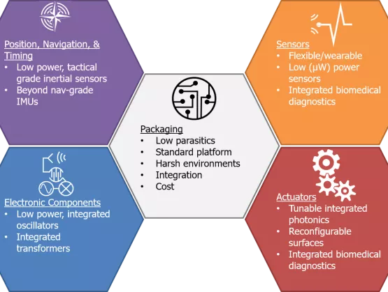
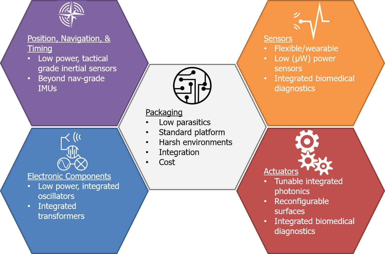
DARPA’s Vision of Cross-CollaborationRon Polcawich, program manager, DARPA Microsystems Technology Office, will give the closing keynote at MEMS Sensors Executive Congress on October 29-30, 2018 in Napa, Calif. SEMI’s Nishita Rao spoke with Polcawich about the MEMS workshop on rapid innovation that he held earlier this year and his interest in continuing that conversation with a broad audience of MEMS and sensors suppliers attending MEMS Sensors Executive Congress. SEMI: What is your vision for the Rapid Innovation through Production MEMS (RIPM) concept and why does the MEMS and sensors industry need it?Polcawich: The goal behind our RIPM concept is to advance the state of MEMS device technology by creating enhanced access to mature process flows for utilization by military, academic and commercial MEMS designers.Compare MEMS to IC development and you will see much more rapid innovation in ICs. In many cases, IC designers can get through four design cycles in a calendar year because the process technologies are so mature.In contrast, it can take three to four years to develop the process flow for a MEMS device. I believe that we can do better. With so much process-flow development in MEMS having taken place over the past 15 years, we now have plenty of commercial designs out there. How do we capitalize on these existing production process flows so we can rapidly innovate to avoid those painfully long production cycles?With this question in mind, we launched a campaign to solicit feedback from small, medium and large foundries, integrated device manufacturers (IDMs), systems designers and integrators, and academic stakeholders. Our effort culminated in a May workshop where we were able to bring many of the same groups to the table. During one intensive day, we discussed challenges to the RIPM concept and what we would need to make it work.SEMI: What were some of your areas of focus?Polcawich: We covered a range of topics, from improving access to sophisticated packaging technology, such as advanced interposer technologies, to IP entanglement and the role of process design kits (PDKs).SEMI: In an industry historically defined by competition over collaboration, how do you hope to convince MEMS supply-chain members to work together?Polcawich: We see benefits from the proposed RIPM concept across the board. Foundries would benefit from outputting higher volumes of devices as well as charging for more sophisticated PDKs and process flows — which would comprise a new source of revenue for them.From our discussions at the workshop and throughout the summer, we understand that certain technology sectors are going to be more willing to engage with the community than others. Notional examples that we highlighted at the workshop include the possibility of manufacturing high-performance inertial sensors, oscillators and pressure sensors within the same process flow. The challenge to the community is having the MEMS designers work within a locked-down process flow and not requesting different material layers, gaps and critical feature dimensions for each device type, which is very common within our industry. We asked everyone the question, “If there were broader access to production process flows, would faster technology transition and innovation cycles enable a more rapid time-to-market for a wider range of products?”SEMI: What would you like MEMS Sensors Executive Congress attendees to take away from your presentation?Polcawich: We welcome additional feedback on the RIPM concept to help shape any potential program ideas. Furthermore, we would like assistance in identifying tipping-point technologies on each sector’s/foundry’s/IDM’s technology roadmap. We could use that information to determine mutual investment opportunities that could shift the roadmap timelines to the left, enabling more rapid production and commercialization timelines. Dr. Ronald Polcawich joined DARPA as a Program Manager in the Microsystems Technology Office (MTO) in August 2017. His research interests include advanced materials processing, micromechanics for small-scale robotics, device designs, and miniaturized position, navigation, and timing (PNT) systems. Read more.Polcawich will present Rapid Innovation with Production MEMS Workshop Outbrief on Tuesday, October 30 at MEMS Sensors Executive Congress in Napa Valley, Calif.Register today to connect with Ron and learn about DARPA’s rapid innovation in MEMS concept.Nishita Rao is a marketing manager at SEMI.
Read More