downloadGroupGroupnoun_press release_995423_000000 copyGroupnoun_Feed_96767_000000Group 19noun_pictures_1817522_000000Member company iconResource item iconStore item iconGroup 19Group 19noun_Photo_2085192_000000 Copynoun_presentation_2096081_000000Group 19Group Copy 7noun_webinar_692730_000000Path
Skip to main content
Default Banner Image

sensors

Most of today’s blockbuster MEMS products – from pressure sensors and resonators to accelerometers and microphones – originated from academic research, a trend that Alissa M. Fitzgerald, Founder Managing Member, A.M. Fitzgerald Associates, expects to continue. While many of these potentially game-changing new technologies will require many more years of intensive development and up to $100 million in investment to reach full commercialization, Fitzgerald sees their potential for generating new waves of activity and opportunity in the MEMS and sensors industry.SEMI’s Maria Vetrano caught up with Fitzgerald to preview her October 23 presentation, Emerging MEMS Sensors Technologies to Watch as We Enter a New Decade, at MEMS Sensors Executive Congress, October 22-24, 2019, at the Coronado Island Marriott Resort Spa in Coronado, California.Join us at MEMS Sensors Executive Congress (MSEC) to meet Alissa Fitzgerald and other industry influencers driving innovation in the MEMS and sensors industry. Register now to connect with her at MSEC or visit her on LinkedIn.SEMI: What are your top three emerging MEMS and sensors technologies with the greatest promise?Fitzgerald: Let’s start by defining emerging. In researching this topic for MSEC, I reviewed a year’s worth of academic papers to search for compelling technologies that will emerge five to 10 years from now. While these applications are not yet commercially ready, they bear a distinct presence in academic literature, and some have even reached the proof-of-concept phase. They all have the potential to advance user functionality derived from MEMS and sensors in very meaningful ways.Next-Generation MicromirrorsI’ve noticed renewed interest in micromirrors, driven by interest in LiDAR for autonomous vehicles, in fiberoptic networking, and in VR/AR glasses and headsets as well.Newer generations of micromirrors will use piezoelectric films to enhance optical performance. Piezoelectric actuation can pivot the mirror to a much larger angle than older-generation electrostatically actuated micromirrors. This is important for wider-angle scanning for LiDAR – as well as for other applications – as it enables the creation of a larger picture image.Piezoelectric films can also be used to change the shape of the mirror surface to enable a variable-focus mirror. This is useful on two fronts: It supports depth-of-field adjustments and it alleviates the need for extreme precision in packaging of optical devices, improving both cost and yield.Event-driven sensors/zero-power/ultra-low power sensorsSensors that draw no power, or that draw just small amounts, by activating only upon a triggering stimulus, are enormously exciting. Their extremely low power consumption addresses one of the most significant obstacles to creating large-area sensor networks: the problem of too-frequent battery changes.In addition, while most sensor nodes today broadcast a large stream of data back to the mother ship by radio, these event-driven or zero-power sensors consume only a small amount of power because they activate the radio only to transmit essential data.Resolving the power-consumption problem with sensors will allow deployment of large-area sensor networks in remote or inaccessible locations, highly useful for applications such as monitoring infrastructure.Bacterial sensorsSensors that can detect the presence of bacteria, as well as the type, have widespread applicability beyond medical uses. They would be particularly useful in food-safety applications as they can identify particular strains of bacteria, such as E. coli, before the beef leaves the processing plant or the spinach ships from the warehouse. This could offer dramatic improvements in food safety over the Centers for Disease Control (CDC) and U.S. Food and Drug Administration’s (FDA’s) food safety program, which only flags foodborne illness when a cluster of people are seriously ill.Researchers are also designing bacterial sensors for rapid point-of-care (POC) diagnostics to detect, for example, sepsis early, potentially saving lives.SEMI: You’ve said that some future MEMS and sensors will use alternatives to silicon. When might we see MEMS and sensors printed on paper or other flexible materials – and for which applications are they suited?Fitzgerald: We’re seeing an enormous amount of development of sensors made on paper, plastics and even textiles, materials that are readily available, inexpensive and flexible.What’s gating our progress right now is manufacturing infrastructure. At present, researchers are using inkjet printers, 3D printers, etc. to manufacture prototype sensors, but in most cases, they would need to move to roll-to-roll printing to scale up. I think that we’re looking at a decade before we see these sensor technologies reach the mass market.When they do arrive, we’ll see sensors that we can easily affix to any kind of carton, wrapper or packaging used with food or other disposable items. Traceability and status of perishable items in particular will allow consumers to track food from the farm or factory to the warehouse, store and, finally, to the home.Implementing these kinds of sensors would also help the environment. According to the Natural Resources Defense Council, in the United States alone up to 40 percent of our food is wasted annually, in part because we fear it’s gone bad. If consumers feel assured that their food is safe, they will waste less. And wasting less means that we can grow less food to feed the same number of people. We’ll also reduce the volume of food waste that goes to landfills.SEMI: What can the MEMS industry do to promote the use of more environmentally friendly materials in its products?Fitzgerald: Some of this is already underway. More companies in our industry are adopting Restriction of Hazardous Substances (RoHS) standards to get rid of heavy metals, such as lead, cadmium or other hazardous materials, in their electronics.We could also produce disposable sensors on paper or on biodegradable plastics, which would decompose within a few months, and we could use safer metals, such as gold, magnesium or zinc, to reduce hazardous metals’ contamination in landfills. While it’s not feasible to make all sensors biodegradable, the market for such sensors could be massive.As companies (and individuals), we should also work hard to design electronics that consume less power, because this ultimately translates to fewer disposable batteries in landfills.SEMI: What would you like MSEC attendees to take away from your presentation?Fitzgerald: I’d like to make two main points. First, the trend to use other non-silicon materials to make MEMS and sensors is real and inevitable. It’s a matter of when. Anyone building a gas or chemical sensor on silicon should look at how to do it on paper or plastic because there are great future applications incorporating flexible, disposable sensors in packaging of all types. That’s the low-hanging fruit.Second, to support this technology development trend, we must look seriously at manufacturing infrastructure because we will need completely different sets of equipment, environments and consumable materials to manufacture MEMS and sensors on paper or plastic. Sensor manufacturers could prepare for this future expansion by beginning to collaborate today with companies that already produce paper and plastic goods. Alissa Fitzgerald, Ph.D., founded A.M. Fitzgerald Associates, LLC (AMFitzgerald), a MEMS and sensors solutions company, in 2003. She has over 20 years of engineering experience in MEMS design, fabrication and product development.Prior to founding AMFitzgerald, Fitzgerald worked at the Jet Propulsion Laboratory, Orbital Sciences Corporation, Sigpro, and Sensant Corporation, now part of Siemens. She received her bachelor’s and master’s degrees from MIT and her doctorate from Stanford University, in Aeronautics and Astronautics. Fitzgerald has numerous journal publications and holds eight patents. She served on the Governing Council of MEMS Industry Group from 2008-2014 and was inducted into the MIG Hall of Fame in 2013. Fitzgerald serves on the Board of Directors of both Rigetti Computing and the Transducer Research Foundation.For more information, please visit AMFitzgerald.MEMS Sensors Industry Group (MSIG), the industry association representing the global MEMS and sensors supply chain, hosts the annual MEMS Sensors Executive Congress. To learn how MSIG enables professionals in the MEMS and sensors industry to innovate, address common challenges and accelerate business results, visit us today.Maria Vetrano is a PR consultant for MSIG, a SEMI Strategic Association Partner.
Read More
Smart cities of the digital future will employ systems enabled by MEMS and sensors in wide-ranging ways. From wearable sensors that monitor personal health and wellness and environmental sensors that assess air quality to autonomous micro-transit systems that are efficient and environmentally sustainable, MEMS and sensors are critically important to living in smart societies.SEMI’s Nishita Rao spoke with Albert P. Pisano, Professor and Dean at UC San Diego Jacobs School of Engineering ahead of his October 24 closing keynote presentation, MEMS and Systems in the Digital Future, at MEMS Sensors Executive Congress, October 22-24, 2019, at Coronado Island Marriott Resort Spa in Coronado, Calif.Join us at MSEC to meet Albert Pisano and other industry influencers driving MEMS and sensors innovations. Registration is open.SEMI: What are some of the most important large-scale system needs of the digital future – and why is MEMS so important in meeting these needs?Pisano: My vision of the digital future is an optimistic one, in which technology is used to assist people in their pursuit of health and happiness. In that digital future, I expect disruption in several key industries that depend on large-scale systems enabled by MEMS – healthcare, retail, transportation and education.Driving these disruptive forces across all four industries is the demand for more relevant real-time information, collected via inconspicuous technologies. Small in size and weight and low in power consumption, what technology other than MEMS delivers these combined attributes?SEMI: How do you envision MEMS in smart cities? What applications and devices will change the human experience in cities?Pisano: Smart cities, by my definition, are cities in which the four basic industries – healthcare, retail, transportation, and education – are implemented in their disrupted form.Take healthcare, for example. The adoption of MEMS chemical sensors in a wearable format will revolutionize human health monitoring. These sensors will not only improve individual health but also mitigate the spread of disease.In transportation, the coming of semi- or fully autonomous vehicles (as well as the general upgrading of all mass-transit vehicles) will give commuters additional time to pursue their interests while en route. A coming revolution of data connectivity to all vehicles will spur the rise of work, study and entertainment options available to people in transit. MEMS in the communication channels as well as in the vehicles will play an essential role in streaming personal data to travelers.SEMI: Could you help us visualize a disruptive application in one of these industries, say healthcare? Pisano: Healthcare is a particularly compelling area because MEMS offers life-enhancing, even life-saving, functionality that will significantly improve the quality of life of some people. MEMS allows us to design consumable wearable sensors that allow individuals to unobtrusively and non-invasively obtain biochemical data, such as potassium, sodium and sugar levels in the body fluid, as well as metabolic indicators such as lactic acid. Further, MEMS-based devices can perform EKG and EEG functions as well as monitor blood pressure in deep body veins in non-medical settings. This higher level of medical-grade data (not just casual data such as an approximate number of steps taken) will allow departments of public health to identify the early onset of individual disease.SEMI: What new forms of wireless communications will affect MEMS-enabled systems in the digital future?Pisano: Most visions of a digital future include wireless communication, but as the spectrum becomes ever more crowded, and as the need for unregulated, negotiated spectrum access increases, we will experience greater pressure to consider other forms of communication, such as inductive, optical and sonic. MEMS sensors are the only technical alternative to these other forms of communication in that they provide acceptable SWAP (size, weight and power). This will spawn battery-powered solutions with significant operational time. A good example is wireless telemetry of human physiological data from the skin. Only MEMS technology can reduce sensor-consumed power to below one microwatt. At this low level, energy harvest from the skin itself is sufficient to power the sensor!SEMI: How is the UCSD campus a living laboratory for intelligent sensing devices and systems?Pisano: Progressive universities, such as the University of California San Diego, understand that they are microcosms of small cities. They have populations during the day of approximately 65,000 people, a myriad of vehicles and a concentrated group of people.Many functions on campus mirror that of a small city. Lecture halls are similar to movie theatres. Student stores and centers are similar to shopping malls. Student residence halls are similar to apartment houses. Many campuses have medical centers, with their own emergency health services and hospitals. As a microcosm of a small city, it is only natural to think of the university as a wonderful living laboratory that allows us to test out new technologies at scale.Clearly, autonomous transit and wearable sensors have potential for uptake in this community. And that’s just scratching the surface. Package delivery (dinner to a dorm room, perhaps?), parking-spot location assistance, and even location-independent data streaming for classroom lectures are just a few possible examples of applications that we can test in a university environment.SEMI: How can the MEMS and sensors industry help researchers and innovators realize the digital future?Pisano: As a MEMS practitioner for almost 30 years, I fully understand the need to focus at the device level to ensure that the MEMS design meets SWAP and other requirements. But I truly believe that MEMS designers must learn to think more about subsystem and system issues, since the future of MEMS will be won by those who cannot only design the device right, but who can design the right device. By taking a much more market- and system-oriented approach to MEMS design thinking, companies in this industry will realize greater success.Register now to connect with Albert Pisano at MSEC and visit his UCSD page for more information.Albert P. Pisano, Ph.D., began his service as Dean of the Jacobs School of Engineering in 2013. He holds the Walter J. Zable Chair in Engineering and serves on the faculty of the departments of mechanical and aerospace engineering and of electrical and computer engineering. Pisano is an elected member of the National Academy of Engineering for contributions to the design, fabrication, commercialization, and educational aspects of MEMS, and is a Fellow of the ASME.Prior to his appointment at UCSD, Pisano served on the UC Berkeley faculty for 30 years, where he held the FANUC Endowed Chair of Mechanical Systems. Pisano was the senior co-director of the Berkeley Sensor Actuator Center (an NSF Industry-University Cooperative Research Center), director of the Electronics Research Laboratory (UC Berkeley’s largest organized research unit), and faculty head of the Program Office for Operational Excellence, among other leadership positions. From 1997 to 1999, Pisano was a program manager for the MEMS Program at the Defense Advanced Research Projects Agency (DARPA). Pisano held several research positions prior to joining academia.Pisano is a co-inventor listed on more than 36 patents in MEMS and has co-authored more than 400 archival publications. Pisano also is a co-founder of 10 startup companies in the areas of transdermal drug delivery, transvascular drug delivery, sensorized catheters, MEMS manufacturing equipment, MEMS RF devices and MEMS motion sensors. Visit his faculty page to learn more about his research interests.MEMS Sensors Industry Group, a SEMI technology community representing the global MEMS and sensors supply chain, hosts the annual MEMS Sensors Executive Congress. To learn how MSIG enables professionals in the MEMS and sensors industry to innovate, address common challenges and accelerate business results, visit us today.Nishita Rao is marketing manager for technology communities at SEMI.
Read More
Software for sensors has evolved from simply reading out and evaluating sensor data to making intelligent decisions based on that data, a transformation enabled by new software synthesis and artificial intelligence (AI) technologies. Together, they make consumer devices smarter, dramatically improving the user experience through greater interactivity and higher levels of automated personalization.SEMI’s Nishita Rao spoke with Stefan Finkbeiner, CEO and General Manager at Bosch Sensortec, who will explore the topic in his October 23 keynote, How Software Makes MEMS Sensors into Smart Systems, at MEMS Sensors Executive Congress (MSEC), October 22-24, 2019, at the Coronado Island Marriott Resort Spa in Coronado, Calif.Join us at MSEC to meet Bosch Sensortec and other industry influencers driving MEMS and sensors innovations. Registration is open.SEMI: What is the relationship between MEMS sensors suppliers and specialized software synthesis providers?Finkbeiner: Collaboration is a key driver for innovation in sensor software. There are already several fruitful collaborations between MEMS sensors suppliers and specialized software providers, which are mostly startups. Collaborations with providers of simulation and evaluation tools as well as with well-known universities in the field of AI are starting to show positive results.Domain expertise is also critical for developing smart sensor software, making it essential to future sensing solutions.SEMI: How does software synthesis relate to sensor fusion?Finkbeiner: Put simply, software synthesis refers to ways of automatically generating code based on domain knowledge and given constraints for specific product versions. Sensor fusion combines sensor data from different kinds of sources in order to improve the results.Software synthesis techniques enable a level of automation that creates new opportunities for more complex sensor fusion, which was formerly out of reach when using traditional approaches that involved, for example, big data and a large number of potential data sources.The traditional sensor fusion toolset can now be further extended by machine learning techniques that help to determine which sources are more reliable than others and how to combine data streams. This topic and others are still active areas of research. A wearable device with motion detection is a case in point. With unsupervised learning, the device could identify short versus long cyclically repeating motions and treat them differently from other types of motion. SEMI: How is the new software synthesis-AI approach different from previous approaches? To what degree will the new approach open up new applications?Finkbeiner: Traditionally, technology companies have used cloud computing for data storage and machine learning on aggregated user data. In that model, MEMS sensors generate large amounts of data that power-hungry hardware (such as digital signal processors) must process. In addition, machine learning generally requires lots of power-hungry cloud nodes with GPUs. This model, however, is not the best option for many users. Just think for a moment about all the scenarios in battery-powered devices where frequent battery charging frustrates users.Leveraging both software synthesis and AI techniques in MEMS sensors is therefore a very promising approach because it supports improved recognition and learning inside the sensor. This means that user-specific data isn’t transferred to the cloud. Instead, it remains private inside the sensor. This improves existing applications that learn all the time and opens up new opportunities for applications such as smart clothing, predicting a product’s lifespan, detecting whether a window or door is open or closed – all without server connectivity.SEMI: How will such software adapt to the individual user?Finkbeiner: Devices will offer much more personalized information to users. For example, optimizing a step counter to match the height, age or Body Mass Index (BMI) of a user – or to adapt to a user’s environment (is the person running on a beach, hiking up a mountain or strolling in a park?) – will provide more accurate information on calories burned. Not every step is created equal, and both pre-loaded personal data as well as real-world environmental data will prove that some steps consume a lot more energy than others.SEMI: What would you like MSEC attendees to take away from your presentation?Finkbeiner: I want to introduce the journey of software development by illustrating specific use case examples. I would also like to offer my outlook on the role of software and AI in MEMS sensors to help increase their adoption in current and new applications. Ultimately, I think it’s important to raise awareness in our industry on why we should embrace the use of software and AI.Connect with Stefan Finkbeiner at MSEC or via LinkedIn. Get more information on Bosch Sensortec products and solutions online.Stefan Finkbeiner, Ph.D., CEO and General Manager, Bosch Sensortec, was appointed CEO of Bosch Sensortec in 2012. He joined the Robert Bosch GmbH in 1995 and has been working in different positions related to the research, development, manufacturing, and marketing of sensors for more than 20 years. His senior positions at Bosch have included director of marketing for sensors, director of corporate research in microsystems technology, and vice president of engineering for sensors.Finkbeiner received his Diploma in Physics from the University of Karlsruhe in 1992 before studying at the Max-Planck-Institute in Stuttgart, where he earned his Ph.D. in Physics in 1995. In 2015, Finkbeiner received the prestigious lifetime achievement award from the MEMS Sensors Industry Group (MSIG), a SEMI technology community.Bosch Sensortec is a member of MEMS Sensors Industry Group, the industry association representing the global MEMS and sensors supply chain. To learn more about how MSIG enables professionals in the MEMS and sensors industry to innovate, address common challenges and accelerate business results, visit us today.Nishita Rao is marketing manager for technology communities at SEMI.
Read More
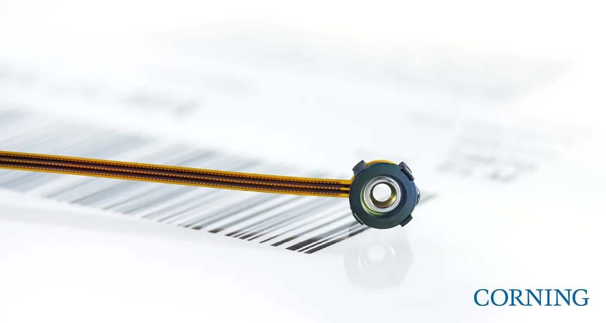
The evolution of industrial and non-industrial automation, smart manufacturing, and Industry 4.0 technologies have increased demand for vision systems that support robust, reliable imaging industrial applications. What factors are driving growth in the machine vision market today?SEMI spoke with Frederic Laune, Business Manager, European Technology, Corning, about how Corning® Varioptic® Lenses are vital to advancing the speed, efficiency, and integration of products using computer imaging. Laune shared his views ahead of his presentation at SEMI MEMS Imaging Sensors Summit, 25-27 September, 2019, at the WTC in Grenoble, France. Join us at the event to meet Corning and many other key industry influencing players. Registration is open.SEMI: Corning's markets include optical communications, mobile consumer electronics, display technology, automotive, and life sciences vessels. Back in June 2019, Corning Incorporated announced that it had delivered its 2 millionth Corning® Varioptic® Lens for industrial applications. What drove this great milestone?Laune: This milestone was met thanks to the fact that Corning Varioptic’s solution solves several problems generated by classical motorized solutions used in industrial applications: limited number of actuation cycles, poor vibration and shock resistance, size (meaning bulky), and high-power consumption. Before Varioptic, there was no variable focus solution that worked well.In addition, the explosion of the CMOS sensor technology helped drive down the cost of imaging solutions for industrial devices, increasing the number of applications and shipping volumes.SEMI: What inspired Corning Varioptic Lenses?Laune: Varioptic was started in 2002 by Dr. Bruno Berge, a French physicist turned entrepreneur. Inspired by the work of Gabriel Lippmann, the 1908 Nobel Prize winner for the invention of color photography, Dr. Berge explored the shape-altering effects of an electric charge when applied to two liquids, a phenomenon referred to as electrowetting. His research ultimately led to the creation of liquid lenses.Fast forward to 2017, when Varioptic became a part of Corning through an acquisition that included Varioptic and Invenios technologies. We believe the synergies from this acquisition will lead to exciting new liquid lens application opportunities that align with Corning’s growth strategy and core capabilities. Corning is one of the world’s leading innovators in materials science. For more than 165 years, Corning has applied its unparalleled expertise in glass science, ceramic science, and optical physics to develop products that transform industries and enhance people’s lives.SEMI: What differentiates traditional camera systems from adjustable lens solutions?Laune: Traditional industrial cameras are usually fixed focus, meaning that the image is sharp only in a limited distance range. Unlike consumer camera applications, there were no good solutions for variable or auto focus cameras in the industrial space. This is due to the intrinsic limitations of motorized technologies.Therefore, customers were using, for example, several cameras to focus at several distances. This compromises the optical quality by closing the objective in order to increase the depth of field, therefore limiting resolution and leading to a need for more light.The cameras using Corning Varioptic’s technology offer more functionality with their ability to focus, whatever the distance, in a fast, reliable, and accurate fashion, and with lower power consumption than traditional mechanical solutions. The upshot is that the product that can withstand heat, vibration, mechanical shocks, and high numbers of focus cycles in tough industrial environments. SEMI: And how is electrowetting enabling industrial devices to capture images and process information quickly and clearly? Laune: In two words: fast and accurate.Electrowetting has unique features – with our two-liquid solution, we combine fast focus with high vibration and shock resistance, and the added benefit of low power consumption.What’s more, our programmable lens can be reconfigured on demand. The lens adapts rapidly and continuously from diverging to converging and can be modeled to support demanding variable focus applications. Our lenses can change their focus in milliseconds, similar to the human eye, and capture fast-moving objects at varying distances. The use of liquid, over mechanical solutions, allows us to create a small form factor, saving precious space and reducing power consumption.SEMI: What industrial applications are taking advantage of this technology? Can you name one example?Laune: 2D barcode readers and industrial vision are our main markets. There is also a strong adoption of our technology in medical applications.SEMI: What does the rise of machine vision mean for manufacturers? Give us one prediction about the opportunities offered by advanced imaging applications.Laune: A great example is the use of 2D barcode readers and liquid lenses to track your ecommerce order, point to point. Another example is full product traceability by implementing a 2D barcode on every component of a given product globally to improve product quality. The varying and adjustable focus abilities of our liquid lens technology make it possible for barcode scanners to track products of different heights, allowing manufactures to improve their processes and logistics.Beyond these examples, tracking and analyzing are booming, thanks to the combination of low-cost CMOS sensor technology, increasing processing power, innovative algorithms (deep learning, AI, neuromorphic processors, etc.), and better image quality due to the progress of lens technology, Varioptic being one.We see an opportunity to improve people’s lives, such as enabling better analysis of medical images and improving the use of cameras in biomedical technologies.SEMI: Quality inspection and automation, adoption of Industrial 4.0 technologies, government initiatives. If you were to choose one, what main factor will drive growth in the machine vision market?Laune: It is difficult to pick just one. I believe that full traceability (monitoring individual parts throughout the production process) has interesting implications as compliance and regulatory efforts ramp up and stronger security of goods becomes more important, particularly as consumers become engaged in food safety and tracing products throughout the supply chain.SEMI: What are your expectations for the SEMI MEMS Imaging Sensors Summit and why would you invite your peers to attend? Laune: I strongly believe in the power of human interactions in technology and science! Ideas come from discussions and physical interactions. The SEMI MEMS Imaging Sensors Summit is a great place to network, meet people, and think about the future! Frederic Laune is the business manager leading the Corning® Varioptic® Lenses business. Laune joined Varioptic as an R D engineer in 2003 after spending the first eight years of his career developing novel active components for the optical telecom industry. At the time, Varioptic was a newly created start-up aiming to develop liquid lens technology for industrial applications. After designing the first two Varioptic commercial products, the Arctic 320 and Artic 416, Laune stepped up as head of Varioptic’s R D department to focus on product and performance improvements. In 2010, he was appointed sales and marketing lead for the company. Varioptic was acquired by Corning Incorporated in early 2017. Laune received a master’s degree in physics and optics from University Pierre and Marie Curie (Paris) in 1995.Serena Brischetto is a marketing and communications manager at SEMI Europe.
Read More
John Smee, VP Engineering, Qualcomm Technologies Inc., will share insights on 5G – which is evolving to enable more reliable connectivity with higher performance in and beyond the era of Internet of Things (IoT) – in his keynote at MEMS Sensors Executive Congress, October 22-24, 2019, in Coronado, Calif.SEMI’s Maria Vetrano caught up with John to give MSEC attendees a preview of his talk.SEMI: Why should MEMS and sensors suppliers stand up and take note of the evolution in 5G, particularly 5G NR?Smee: 5G is the unifying fabric that will connect virtually everything around us. 5G New Radio (NR) is the global standard for a unified, more capable 5G wireless air interface. It will deliver significantly faster and more responsive mobile broadband experiences to users. It will also extend mobile technology to connect and redefine a multitude of new industries, including the IoT.As tens of millions of MEMS and sensors are the core components providing intelligence and interactivity to IoT devices, suppliers need to understand the capabilities and efficiencies that 5G will bring to connect the wide range of MEMS and sensors.We should also recognize that we are at the beginning of the 5G era, and 5G technologies will continue to evolve and expand in the coming years to connect new types of devices in increasingly efficient ways.SEMI: What’s special about the upcoming release of 5G NR, 3GPP Rel-16?Smee: While the first 5G NR release, 3GPP Rel-15, focused primarily on enhanced mobile broadband (eMBB), it also established a solid technology foundation for continued evolution in Rel-16 and beyond.With Rel-16, we are seeing 5G NR’s expansion beyond eMBB to address new tiers of IoT services such as industrial IoT (e.g., automation) with ultra-reliable, low-latency communication (URLLC) and cellular vehicle-to-everything (C-V2X) for more advanced use cases, such as autonomous driving. MEMS and sensors are critically important to both types of use cases as they collect the raw information of the physical world, and 5G is the connectivity of these sensors to the network. This makes the technologies inextricably linked.MEMS and sensors are equally integral to the development of more efficient low-complexity massive IoT devices (MIoT) with in-band 5G NR deployments of enhanced machine-type communication (eMTC)/narrowband Internet of Things (NB-IoT) and the use of the new 5G Core Network. In practical terms, devices that enable smart city use cases – such as smart utility monitoring, connected parking meters, and smart street lighting solutions that support 3GPP Rel-16 – are MIoT devices that will delight city administrators and dwellers with their improved coverage and efficiency. SEMI: In addition to low-complexity MIoT devices, what other markets will benefit most from the evolution in 5G NR?Smee: We continue to enhance 5G NR to support the high-performance IoT, including URLLC.URLLC is one of the many new 5G capabilities that wasn’t possible with the previous generation of cellular technologies, such as LTE. Because it delivers services at very high reliability (i.e., 99.9999%) and ultra-low latency (i.e., sub-1ms), URLLC literally opens up new use cases that that only wired communication could serve in the past. Industrial IoT applications that require a mix of high reliability and low latency, such as robotic arm command and control, are foremost among these new URLLC use cases.Another example of IoT taking advantage of URLLC is smart grid, where faults in the electricity distribution network require immediate protection and control to ensure safety and avoid equipment damage.SEMI: How is Qualcomm building on the eMTC/NB-IoT for low-power wide-area IoT (LPWA) – and how will this influence IoT connectivity?Smee: We continue to evolve eMTC/NB-IoT beyond its initial 3GPP release in Rel-13, making these foundational LPWA IoT technologies more capable and efficient as they become the basis for 5G massive IoT.The most significant updates to eMTC/NB-IoT include multi-cast and positioning support in Rel-14 and improved spectral/power efficiencies in Rel-15. Multi-cast can help service providers to deliver firmware updates over the air with greater efficiency, which speeds deployment of new features. Positioning can create new values, which can inform end users where their assets/packages are located, potentially safeguarding assets in transit. Improving spectral/power efficiencies offers more power-efficient transmissions, which takes less toll on battery-operated devices.With Rel-16, we have further optimized eMTC/NB-IoT, which is supported by the new 5G Core Network and is also deployable in 5G spectrum in-band with other 5G NR services.The evolutionary path ahead for eMTC/NB-IoT enables support for an even wider range of 5G massive IoT devices. New enhancements in the pipeline, such as grant-free uplink and multi-hop mesh, will boost efficiency and coverage area that much more.SEMI: Where do mobile broadband devices such as ultra-high-definition (UHD) security cameras fall within Qualcomm’s realization of 5G-NR?Smee: Mobile broadband is at the core of 5G NR. We see it both powering the new generation of 5G smartphones and expanding beyond traditional devices (including always-connected PCs and tablets) to address the needs of high-performance IoT devices such as UHD security cameras.It’s actually an important part of our vision for 5G to have an industrial network that requires all types of 5G connectivity for devices spanning eMBB (e.g., cameras, laptops), URLLC (e.g., machines) and MIoT (e.g., sensors).SEMI: What can the MEMS and sensors industry do to prepare for the 5G wave?Smee: Because 5G can evolve to deliver even better performance and efficiency for connecting sensors in the 5G world, we will see even more widespread adoption of MEMS and sensors into larger numbers of connected applications. MEMS and sensors suppliers, therefore, need to get ready for the 5G wave by preparing to support 5G connectivity in their devices, which will ultimately help to realize the 5G vision of connecting virtually everything in the world around us.John Smee, Ph.D., is vice president of engineering at Qualcomm Technologies Inc., where he is the 5G R D lead responsible for overseeing all 5G research projects, including end-end systems design and advanced RF/HW/SW prototype implementations in Qualcomm’s wireless research and development group. He joined Qualcomm in 2000, holds over 100 U.S. Patents, and has been involved in the design, innovation, and productization of wireless communications systems such as 5G NR, 4G LTE, 3G CDMA, and IEEE 802.11. He also leads Qualcomm’s companywide academic collaboration program across technologies including wireless, semiconductor, multimedia, security and machine learning. John was chosen to participate in the National Academy of Engineering Frontiers of Engineering program and received his Ph.D. in electrical engineering from Princeton University and also holds an M.A. from Princeton and an M.Sc. and B.Sc. from Queen’s University.Smee will present Evolving 5G NR to Connect the Internet of Things on Wednesday, October 23, 2019, at MEMS Sensors Executive Congress, Coronado Island Marriott Resort Spa in Coronado, Calif.Register today to learn how 5G NR will transform the user experience with MEMS- and sensors-enabled devices in IoT, automation and beyond.Interested in engaging with the MEMS and sensors supply chain? MEMS Sensors Industry Group is a SEMI technology community that enables the MEMS and sensors industry to innovate, address common challenges and accelerate business results.Maria Vetrano is a public relations consultant for SEMI.
Read More
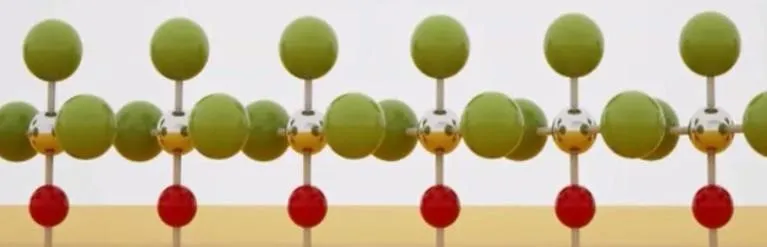
SEMI spoke with Dr. Mikko Söderlund, sales director for Beneq’s semiconductor business, about trends in Atomic Layer Deposition (ALD) applications. Söderlund shared his views ahead of his presentation at SEMI MEMS Imaging Sensors Summit, 25-27 September, 2019, at the WTC in Grenoble, France. Join us at the event to meet Beneq and other key industry influencers. Registration is open.SEMI: The Backside Illuminated (BSI) CMOS Image Sensors (CIS) market continues to experience steady growth. Which applications are currently driving market growth?Söderlund: BSI CMOS Image Sensor market continues to be driven by mobile, security, automotive and Internet of Things (IoT) applications – so there seems to be plenty of opportunities for BSI CIS market to grow further.SEMI: What is critical for advanced thin-film deposition methods to extract best electrical performance?Söderlund: It is critical to control the material properties of the deposited layer (such as charge density, resistivity or barrier property) and of course, film uniformity and conformality. Furthermore, controlling material interfaces is also important, especially for sensitive III-V materials. {% video_player "embed_player" overrideable=False, type='scriptV4', hide_playlist=True, viral_sharing=False, embed_button=False, width='350', height='197', player_id='12721134435', style='margin: 0px auto; display: block; float: right; margin-left: auto; margin-right: auto; width: 350px;' %} Coatings and material features based on existing standard techniques can be very expensive, or not feasible at all. What does Atomic Layer Deposition (ALD), as a thin film coating method, offer in particular?Söderlund: ALD offers dense, highly conformal and pinhole-free best-in-class functional layers for dielectrics, passivation, encapsulation and much more. As a gentle and precise layer-by-layer method, ALD is extremely well-suited for deposition of such performance critical layers over large surface areas such as a cassette of wafers.SEMI: Please describe the Atomic Layer Deposition (ALD) coating process. Söderlund: ALD is based on a self-limiting surface reaction controlled thin film deposition. During coating, two or more chemical vapors or gaseous precursors react sequentially on the substrate surface, producing a solid thin film (see schematic below). Most ALD coating systems use a flow-through traveling wave setup, where an inert carrier gas flows through the system and precursors are injected as very short pulses into this carrier flow. The carrier gas flow takes the precursor pulses as sequential waves through the reaction chamber, followed by a pumping line, filtering systems and, eventually, a vacuum pump.SEMI: What are the two leading edge ALD applications?Söderlund: Today’s leading-edge ALD applications are in logic (high-k/metal gate, multiple patterning) and memory (DRAM capacitor, 3D NAND). Within the More-than-Moore (MtM) markets, CIS and MEMS (actuators and sensors, RF) have been early adopters of ALD, and we also see ALD being introduced in GaN Power and RF, as well as photonics.SEMI: Give us one prediction about the opportunities offered by advanced imaging applications.Söderlund: The large diversity of imaging applications will continue to drive growth and innovation. For example, machine vision is expected to transform the imaging landscape. We see this as a big opportunity for advanced thin-film deposition methods such as ALD, provided that the tools are versatile enough to address the diverse manufacturing requirements.SEMI: What are your expectations for SEMI MEMS Imaging Sensors Summit and why do you invite your peers to attend? Söderlund: The summit brings together all key RF stakeholders in the MEMS and imaging sensors industry, and we are looking forward to a great event. It’s a special event for us as we are officially launching a new ALD cluster tool product specifically engineered for the MtM applications – so this brings great excitement that we want to share with the attendees.Dr. Mikko Söderlund is Sales Director for Beneq’s semiconductor business. He has more than 20 years of experience in product development, product management, technical sales and business development across the photonics, OLED, and semiconductor industries. Mikko received his Ph.D. in Micro- and Nanotechnology from the Helsinki University of Technology. Serena Brischetto is a marketing and communications manager at SEMI Europe.
Read More
The BioMEMS market is becoming increasingly diverse, encompassing gas and pressure sensors, ultrasound, specialized biomedical sensors, and other types of MEMS and microfluidic chips used for drug delivery and analytical applications. The BioMEMS market is also growing steadily: Research firm Yole Développement predicts that BioMEMS will grow at 14.9% CAGR from 2017-2023, reaching US$6.9B by 2023.1 As a high-value market, BioMEMS is worth pursuing as long as you can manage the complexities of manufacturing, including a sometimes-fragmented supply chain. Fortunately, the MEMS manufacturing ecosystem is evolving to accommodate the needs of companies that are in the process of commercializing BioMEMS-enabled products. Understanding the ecosystem’s shifting dynamics will help BioMEMS to flourish in this promising while often-challenging market segment.Unique Product, Unique ProcessIn the world of semiconductor manufacturing, it is routine for a fab to manufacture hundreds of different device designs using just a handful of process nodes. Semiconductor foundries share their design rules with customers, who then develop the mask set accordingly, literally adapting their designs to fit the rules for manufacturing on one of the foundries’ process nodes. In stark contrast, most MEMS devices cannot conform to the level of standardized manufacturing processes that work so well for semiconductors. Rather, MEMS challenges us to develop individualized processes for each device. It’s one product, one process.New BioMEMS designs generally emerge from either corporate R D or academia, two groups that approach specialized MEMS foundries such as ours when they’re entering pilot or low-volume production. Today successful commercialization depends on open, accurate communication and close collaboration. MEMS foundries must work side-by-side with designers to ensure that designs are based on real-world manufacturing process technologies. This highly customized manufacturing model makes it very difficult to support future demand for the groundswell of diverse BioMEMS devices that are in development. If we want to handle this upward trajectory of BioMEMS, we’ll need to adapt.Change the ModelWhile most existing MEMS foundries currently support a wide variety of devices types, I predict that market forces will cause our foundries to move toward specialization. Some companies will specialize in what they already do best, e.g., inertial sensors for the automotive industry. Others might choose to develop their foundry business around a purpose-built facility, which, for example, only manufactures microfluidics or magnetic devices. Larger enterprises might opt to build captive foundries that are designed to serve their specific needs. Get Creative: Combine, CollaborateSatisfying the thriving market for BioMEMS will require creativity. One idea: combine different disciplines of the manufacturing process at the same foundry. For example, we could have a biochemistry fab and a MEMS fab under the same roof, or we could have a MEMS fab and a packaging facility in one building. While these approaches may not yet exist outside of academia, necessity may drive them to fruition.It will also require heightened strategic collaboration, a process that has already begun. To support both large volumes and greater diversity of devices, some MEMS foundries are building cooperative relationships with former competitors. Think of it as a restructuring of the supply chain.Embracing the special challenges of BioMEMS manufacturing is worth our investment in time and resources. We need to step back, individually and collectively, to understand where each of the existing MEMS foundries fits into the new supply chain so we can leverage our strengths. We can start by forging stronger alliances for tech transfer. Once we more freely share information as we engage in joint product development — involving technology teams who are more connected and less guarded — we will expedite tech transfer and manufacturability.While we are unlikely to achieve the same level of standardization that has enabled the semiconductor industry to reach its great heights, as long as we evolve to meet demand, we will grow together and prosper.To learn more about this topic, meet with Jessica Gomez at the upcoming SEMI-MSIG MEMS Sensors Executive Congress (October 22-24, 2019 in Coronado, Calif.) or email her: [email protected][1] “BioMEMS Emerging Non-Invasive Biosensors: Microsystems for Life Sciences Healthcare 2018 Report,” Yole Développement, https://yole-i-micronews-com.osu.eu-west-2.outscale.com/uploads/2018/08/Sample-BioMEMS-Non-Invasive-Sensors-Microsystems-for-Life-Sciences-Healthcare-2018-.pdf As founder and CEO of Rogue Valley Microdevices, Jessica Gomez has created a world-class precision MEMS foundry and wafer fab in the heart of Southern Oregon. Integral to her role as CEO, Ms. Gomez practices a business philosophy of offering custom design, best-in-class process technology and R D expertise to customers, to help them achieve the highest quality and reliability in their products.In 2018, Ms. Gomez was selected for the prestigious SEMI Board of Industry Leaders. SEMI also recognized her in its first Spotlight on SEMI Women, which honors accomplished women in the global microelectronics industry.Prior to founding Rogue Valley Microdevices in 2003, Ms. Gomez honed her experience in semiconductor processing and production management through positions at Standard Microsystems Corporation, Integrated Micromachines and Xponent Photonics.For more information, visit: https://roguevalleymicrodevices.com/Rogue Valley Microdevices is a longtime member and supporter of SEMI-MEMS Sensors Industry Group, which connects the MEMS and sensors supply network, allowing members to address common industry challenges and explore new markets.
Read More
Automotive original equipment manufacturers (OEMs) and their direct suppliers of parts and systems share a vision: Next-generation vehicles will be more electric, autonomous and connected. At a market size of more than $1 trillion, automotive is steadily becoming a high-tech market as cars morph into advanced technology platforms with partially or fully autonomous features. Call them semiconductors on wheels. Big players such as Google and many carmakers are investing heavily in chip advances to help drive increases in silicon content in automobiles.At SEMICON Europa, Pierrick Boulay, Solid State Lighting and Lighting Systems analyst at Yole Développement, will provide a market update on autonomous automobile trends including the state of sensors, radars, cameras and LiDARs as the industry works to increase the level of autonomy and electrification.Autonomous vehicle design can only thrive with the development of an industry standard for chip and device traceability across the supply chain. The importance of chip traceability to the automotive industry is reflected in its central role in driving a chip traceability standard.According to Heidi Hoffman, senior director of technology communities marketing at SEMI, “chip traceability is one of the next big things for the technology industry. The benefits are enormous, and the upsides – including yield enhancements, counterfeiting safeguards, and support for new applications – are plentiful. But the implementation challenges of chip traceability are also big and will require considerable effort to overcome. The biggest hurdle of all? We need to transcend industry fears by demonstrating that we can secure IP when it is shared across the hardware supply chain.” The Importance of Standards, Data Collection and Collaboration Across the Supply ChainThe automotive industry has long embraced tracing the sources of defects. Now, as the automotive and semiconductor supply chains increasingly overlap, traceability has taken on greater importance in the semiconductor industry. SEMI committees, task forces and events such as the Smart Transportation Forum at SEMICON Europa are ideal platforms for collaborating to develop new standards and best practices for the automotive industry.Earlier this year, German luxury automobile maker Audi AG became the first automotive original equipment manufacturer (OEM) to join SEMI as member, strengthening alignment across automotive supply-chain segments. At SEMICON Europa, the SMART Transportation Forum and Pavilion, staged by the SEMI Global Automotive Advisory Council (GAAC) and bolstered by the Electronic System Design Alliance, a SEMI Strategic Association Partner, will gather key stakeholders across the automotive value chain, from design and semiconductor equipment to materials and carmakers, to explore innovation opportunities in automotive electronics. SEMI Global Automotive Advisory Council (GAAC) “If the industry wants to reach the goal of zero defects, a new collaborative approach is necessary,” observed Antoine Amade, senior regional director EMEA at Entegris. At SEMICON Europa, Amade will present new ways to collaborate in reducing chip defectivity and meet other challenges in the automotive industry.More than half of semiconductor failures on the automotive assembly line today (so-called 0km failures) are traced to semiconductor fab defectivity. “The increasing semiconductor content in automobiles – driven by growth in ADAS, electrification and autonomy – has put a growing focus on the quality and reliability of these devices and their implications for consumer safety and satisfaction,” said Oreste Donzella, senior vice president and CMO at KLA.The smart manufacturing (Industry 4.0) revolution is already spurring higher performance and great efficiencies throughout the supply chain and will also be crucial to driving innovation in automotive. Smart manufacturing makes possible significant improvements in factory key performance indicators (KPI) for cycle time, on-time delivery, overall equipment effectiveness, cost and product quality.“These KPI gains are key to meeting quality levels the automotive industry must reach to support the deployment of autonomous driving vehicles,” said John R. Behnke, general manager of Final Phase Systems at INFICON. In his talk at SEMICON Europa, Behnke will provide an overview of existing, in-progress, and future smart manufacturing solutions for the semiconductor industry and their impact on the automotive supply chain. The SMART Transportation Forum, 13 November, 2019 (9:30-15:30 at ICM Munich, room 14c) at SEMICON Europa is the premier platform for key stakeholders to connect, collaborate and innovate across the automotive value chain. Automotive and semiconductor industry experts will offer insights into trends in design, semiconductor equipment and materials, and automotive innovation and the roadmap to 2030. The SMART Transportation Forum will also showcase innovations in imaging, sensing, artificial intelligence (AI), smart manufacturing and L5 mobility.Other SEMICON Europa highlights: Advanced Packaging Conference: Packaging and Test Challenges Towards High Reliability (12-13 November 2019) 23rd Fab Management Forum: Game Changers for Semiconductor Operations(11-12 November 2019) Strategic Materials Conference: Strategic Materials Enabling Industry Roadmaps(12-13 November 2019) SEMICON Europa registration is open for visitors and exhibitors. For more details, please visit the SEMICON Europa website and connect with SEMI Europe on Twitter or LinkedIn @SEMIEurope (use #SEMICONEuropa).Learn more about the SEMI chip traceability standard – SEMI T23 - Specification for Single Device Traceability for the Supply Chain – and SEMI Technology Communities.Serena Brischetto is a marketing and communications manager at SEMI Europe.
Read More
Stefano Zanella, Head of Automotive, Industrial and Location Businesses, TDK InvenSense will present at next month’s SEMICON Taiwan (September 18-20, 2019 in Taipei City, Taiwan). SEMI Taiwan’s Emmy Yi spoke with Stefano for a preview of his talk.SEMI: What macro market trends are driving automotive manufacturers to increase the variety and volume of MEMS sensors in cars?Zanella: The car world is changing. Consumers increasingly view car ownership as less desirable, yet the number of miles traveled and of hours spent in a car are rising steadily. At the same time, cars are changing profoundly, and the pace of change is rapid. To thrive in this new world, automakers are becoming transportation enablers and providers.Many vehicles today autonomously interact with humans and the world around them, operate with less or no human control, and are powered by electric batteries. MEMS sensors – which mimic and augment the five human senses – are front and center in these advancements.Unlike other types of sensors – such as cameras, radar and GNSS/GPSS – MEMS gyroscopes are functional in every environment. Gyroscopes, as well as accelerometers, can supplement those other sensors when they are not available and boost the accuracy of their outputs when they are available. Both camera stabilization and dead reckoning when GNSS is unavailable are good examples of the latter. Other prevalent sensors include MEMS microphones, used to capture voice commands, ultrasonic sensors, which can be leveraged for parking and gesture recognition, and fingerprint sensors, which can improve car security.SEMI: How can automakers stay competitive in this changing landscape?Zanella: Automakers can future-proof their relevance in the transportation market in several ways. By embracing consumer migration toward ride-sharing over car ownership, many are transforming from manufacturers to mobility providers. Carmakers that invest in ride-sharing and other modes of transportation (e.g., scooters) can sustain their profitability, even if the number of vehicles sold eventually shrinks or simply doesn’t grow as much as anticipated.Automakers will need to pursue new avenues of product differentiation. Traditionally, automakers have kept performance and aesthetics to themselves by owning the engine and the body design of the car, leaving nearly everything else to suppliers. Autonomous driving and electrification, however, are pushing automakers to own the battery pack and the autonomous driving software stack.While we are just beginning to see standardization in battery packs, automakers are likely to own the autonomous driving stack for many years to come. Automakers that offer cars with highly functional and efficient batteries and driving stacks stand to gain market share.Automotive infotainment systems will become increasingly crucial as autonomous driving turns everyone into a passenger. Audio subsystem providers such as Harman Kardon, Bose, and Bang Olufsen, for example, jockeyed for attention at the most recent Geneva Motor Show, demonstrating sophisticated surround-sound systems that rival premium-quality home audio setups.With more and more consumers using voice interfaces to interact with devices in the home, drivers are less willing to accept spotty accuracy in the car. Hence, automakers are using more higher-performing MEMS microphones to accurately capture voice commands. This will come as a relief to those of us who routinely yell at our steering wheels while using voice command to try to call home. Demand for higher quality infotainment systems has prompted some automotive OEMs to own the entire infotainment system and work directly with sensor and chipmakers, a level of intimacy that gives automakers a chance to tune sensor and chip development to their own needs. This tighter relationship also positions device suppliers to forge more direct links with drivers.SEMI: Which MEMS sensors are particularly important to tomorrow’s automobiles and why?Zanella: For many years the automotive industry has been integrating more electronics into cars to improve safety, advance the driver and passenger experience, and, more recently, power the car. As vehicles rely less on human control, automakers must replace the senses of the driver with something else. That something else is a bunch of sensors, microphones, cameras, radar and LIDAR to replace vision and hearing.Since MEMS sensors such as accelerometers, gyroscopes and pressure sensors are much more robust than other types of sensors to operate in snow, rain and darkness and other imperfect environments, automakers use them to ensure that the vehicle never gets lost when other sensors and/or the GPS/GNSS signal become unavailable in tunnels or urban canyons. Gyros help determine direction, accelerometers velocity and distance driven, and pressure sensors height, such as when taking a fork on a multi-level highway. At the same time, fingerprint sensors, ultrasonic parking sensors, and temperature sensors are improving convenience, safety and security for the car’s occupants. Automakers increasingly use inertial and environmental sensors, MEMS microphones, fingerprint sensors, and vision/imaging sensors to augment or replace the five human senses on which car drivers have relied for over 100 years. Source: TDK InvenSense SEMI: To what degree can MEMS sensors enable automotive security?Zanella: MEMS sensors are used widely to enhance security today. Some of their mechanisms are easy to understand while some are unexpected. For instance, ultrasonic fingerprint sensors can authenticate the driver of a vehicle to prevent car theft or something less onerous, like a teenage driver taking the car out without permission.Accelerometers and gyroscopes can prevent a new type of spoof on keyless entry systems. Imagine that you are very close to your vehicle. Your car senses the remote control in your pocket and automatically opens the doors when you pull the handle. Now suppose that your car is parked on the street, not far from your house. You leave the remote control home, and the car doesn’t sense the proximity of the remote control. Great! No one can enter your car, unless ... a thief has a big signal amplifier that makes your car think that the keyless entry device is next to the car. In this case, what can an automaker do? Add an accelerometer that restricts the keyless device from broadcasting the entry signal unless you are walking to the car with the device on your person.SEMI: What would you like SEMICON Taiwan attendees to take away from your presentation?Zanella: I would like them to embrace the transformations afoot in the automotive market as well as their associated design challenges since, by overcoming these hurdles, they can offer significant societal benefits such as safer and cleaner transportation. At the same time, these transformations mean significant opportunities for semiconductor industry revenue growth. And while design-to-delivery cycles in automotive are longer than in consumer and mobile, the automotive market supports higher-value devices as well as the chance to fold dozens of MEMS sensors into a single model.To paraphrase Lord Kelvin: If you can’t sense it, you can’t manage it. As suppliers of many key technologies that make intelligent transportation possible, the MEMS sensors industry is in an excellent position to help automakers manage the many challenges ahead.Stefano Zanella, Ph.D., is Head of Automotive, Industrial and Location Businesses at TDK InvenSense, where he brings MEMS sensors (including accelerometers, gyroscopes and microphones) and location solutions to the automotive and industrial markets. Zanella holds an MS and a Ph.D. in Electrical Engineering from the University of Padova, Padova, Italy as well as MBAs from both the UC Berkeley Haas School of Business and from Columbia University.He will present MEMS Sensors Enabling the Smart Car Revolution on Wednesday, September 18, 2019, at SEMICON Taiwan at 1F 4F, Taipei Nangang Exhibition Center, Taipei City, Taiwan. Register today and save 20% to learn how MEMS sensors are transforming the human experience with cars.Connect with Stefano Zanella at SEMICON Taiwan or via LinkedIn. You can also get more information on TDK’s automotive solutions and application guides online.Interested in engaging with the MEMS sensors supply chain? SEMI MEMS Sensors Industry Group is a technology community that enables professionals in the MEMS and sensors industry to innovate, address common challenges and accelerate business results.Emmy Yi is a marketing specialist at SEMI Taiwan.
Read More
Despite market saturation and stagnation saddling many business sectors, MEMS remains a shining star in the semiconductor industry. Opportunities in automotive, consumer electronics, mobile, medical are rising. What is supporting this industry growth? Who are the big players on the horizon?SEMI spoke with Dimitrios Damianos, Technology Market Analyst, Photonics, Sensing and Display division at Yole Développement, about MEMS market dynamics and future trends. Damianos shared his views ahead of his presentation at SEMI MEMS Imaging Sensors Summit, 25-27 September, 2019, at the WTC in Grenoble, France. Join us at the event to meet experts from Yole and many other key industry influencers. Registration is open.SEMI: MEMS and sensors is one of the healthiest industries not only in Europe but globally. Despite a global economic slowdown, the MEMS and sensors is still growing. What is fueling this growth?Damianos: The value of the global MEMS and sensor market will almost double from $48 billion in 2018 to $93 billion in 2024. In 2018 the MEMS and sensor market represented more than 10% of the total IC market, as more and more MEMS devices and sensors, such as MEMS, image sensors, and RF filters, are integrated in end products in consumer and automotive. In particular, the value of the MEMS-only market reached $11.6 billion in 2018, with consumer applications accounting for more than 60% of the total market. From 2019 to 2024 the MEMS market will grow 8.3% annually in value driven by pressure (for TPMS), RF (for V2X 5G communications), inertial (for ADAS) and future MEMS (such as pMUT for ultrasonic fingerprint) (Source: Status of the MEMS Industry report, Yole Développement, 2019). SEMI: How are MEMS shaping the semiconductor industry today? Damianos: MEMS have a make-smarter enabling capability. They are providing context for new applications and services in transportation, mobility, health, and security. Large companies such as Alibaba and Google are considering MEMS as a critical element in their business solution domains covering the upcoming smart home, smart campus, smart city and smart industry applications. MEMS have key features that correspond to these companies’ criteria for accuracy, small size (without performance degradation), low power and always on (e.g. microphones). Furthermore, with the advent of sensor fusion and edge computing, more sensor data can be processed, maximizing the qualitative and useful information about us and our surroundings. This has a huge impact in all markets, especially consumer.SEMI: MEMS foundries performed well thanks to the boom in industrial and medical applications. Who are the big players right now?Damianos: During 2018, all foundries saw their revenue increase. STMicroelectronics, Teledyne Dalsa, Silex, IMT, Micralyne and Philips Innovation Service are important MEMS foundry players that offer services for various MEMS devices used in medical and industrial markets, among others. On one hand, medical applications were driven mostly by microfluidics, flowmeters, pressure and inertial MEMS. On the other hand, industrial applications were driven by inkjet heads, microbolometers and pressure MEMS. The market prospect, however, is huge for RF MEMS and oscillators that will be used in next-generation 5G infrastructure. SEMI: What is the current status of MEMS for automotive applications? What are the related market drivers? Damianos: In automotive applications, accelerometers and pressure sensors still account for the lion’s share in units. Pressure sensors will grow at more than 8% with Tire Pressure Monitoring System (TPMS) implemented in Chinese vehicles in the near future. After 2019 and 2020, with the new Chinese standard, GB 2614, TPMS will become compulsory: 100% of all new vehicles will have TPMS. Also, automotive MEMS could grow quicker than the corresponding car market (currently at approximately 3%). The reason is a higher number of many different MEMS devices that are being integrated in cars, such as MEMS inertial measurement units (IMUs), TPMS, environmental MEMS for gas and particle monitoring in-cabin and microphones for hands-free voice commands.SEMI: After years of decline, the inkjet heads industry is growing again. What other segments are benefiting from MEMS technology applications? Can you name two examples?Damianos: RF MEMS (BAW filters) is also benefiting from applications in smartphones and will continue to benefit with the arrival of 5G. 5G means additional high frequency sub-6 GHz bands that can only be addressed by BAW filters. Moreover, new infrastructure approach using active antennas will create an expanding market for BAW.Another segment is inertial sensors. Inertial MEMS already have a high potential in wellness and fitness wearables and are gaining support for medical wearable applications to monitor patient activity, with the aim to prevent seizure in cases of epilepsy and other mental disorders. Compared to other types of sensors, MEMS is the golden technology for inertial sensors integrated into medical wearables. They are used for rehabilitation systems, activity trackers and assistance living/fall detection. Specifically, the IMU market will continue to grow for consumer and automotive applications as their price and form factor continue to shrink and they replace traditional standalone MEMS accelerometers and gyroscopes. However, the inertial sensor market will mostly grow for smartphone applications (mostly 6DOF, with 9DOF volumes being comparatively low).SEMI: Give us one prediction about the opportunities offered by the MEMS technology. Damianos: Sensor fusion is becoming more and more relevant since billions of MEMS sensors are made every year. The upcoming 5G revolution will make connectivity easier than ever, creating exponentially more data. To make these data meaningful, data processing is mandatory. Big data is an industry born of recent advancements in AI and machine learning, built upon and fueled by a wealth of new data from ever-expanding sensor applications. An upcoming trend is edge computing, with sensors and MEMS driving a new age of technology. Sensors are digitizing the human experience, and as the real and virtual worlds move closer together, it will be sensors that bind them, enabling new experiences for users everywhere. Running AI at the edge, coupled with sensor fusion, will open new applications for MEMS in audio, motion, olfactometry, and imaging. We also expect that new MEMS devices (microspeakers, ultrasonic fingerprint, pMUT) and piezoelectric MEMS technology could rejuvenate the MEMS market. SEMI: What are your expectations for SEMI MEMS Imaging Sensors Summit and why would you invite your peers to attend? Damianos: SEMI is organizing another very successful event, gathering experts from the Imaging and MEMS industries. We are at a turning point of innovation, with many technological advancements in AI, IoT, AR/VR, biometrics, and other areas where Imaging and MEMS technologies are paramount. Yole is excited to hear the thoughts of many high-profile experts on existing activities and future prospects within their organizations. If you are too, then it is an event that you shouldn’t miss!Dimitrios Damianos, Ph.D. is a Technology and Market Analyst in the Photonics, Sensing and Display division at Yole Développement (Yole). Damianos is a member of a Yole team that produces technology and market reports on the imaging industry including photonics and sensors. Damianos holds a MSc degree in Photonics from the University of Patras (Greece). After his research on theoretical and experimental quantum optics and laser light generation, Dimitrios pursued a Ph.D. in optical and electrical characterization of dielectric materials on silicon with applications in photovoltaics and image sensors, as well as SOI for microelectronics at Grenoble’s university (France). He has also authored and co-authored several scientific papers in international peer-reviewed journals. Learn more! Join the webinar on 5th September 2019. Registration is open! Serena Brischetto is a marketing and communications manager at SEMI Europe.
Read More