downloadGroupGroupnoun_press release_995423_000000 copyGroupnoun_Feed_96767_000000Group 19noun_pictures_1817522_000000Member company iconResource item iconStore item iconGroup 19Group 19noun_Photo_2085192_000000 Copynoun_presentation_2096081_000000Group 19Group Copy 7noun_webinar_692730_000000Path
Skip to main content
Default Banner Image

Smart Manufacturing

read more

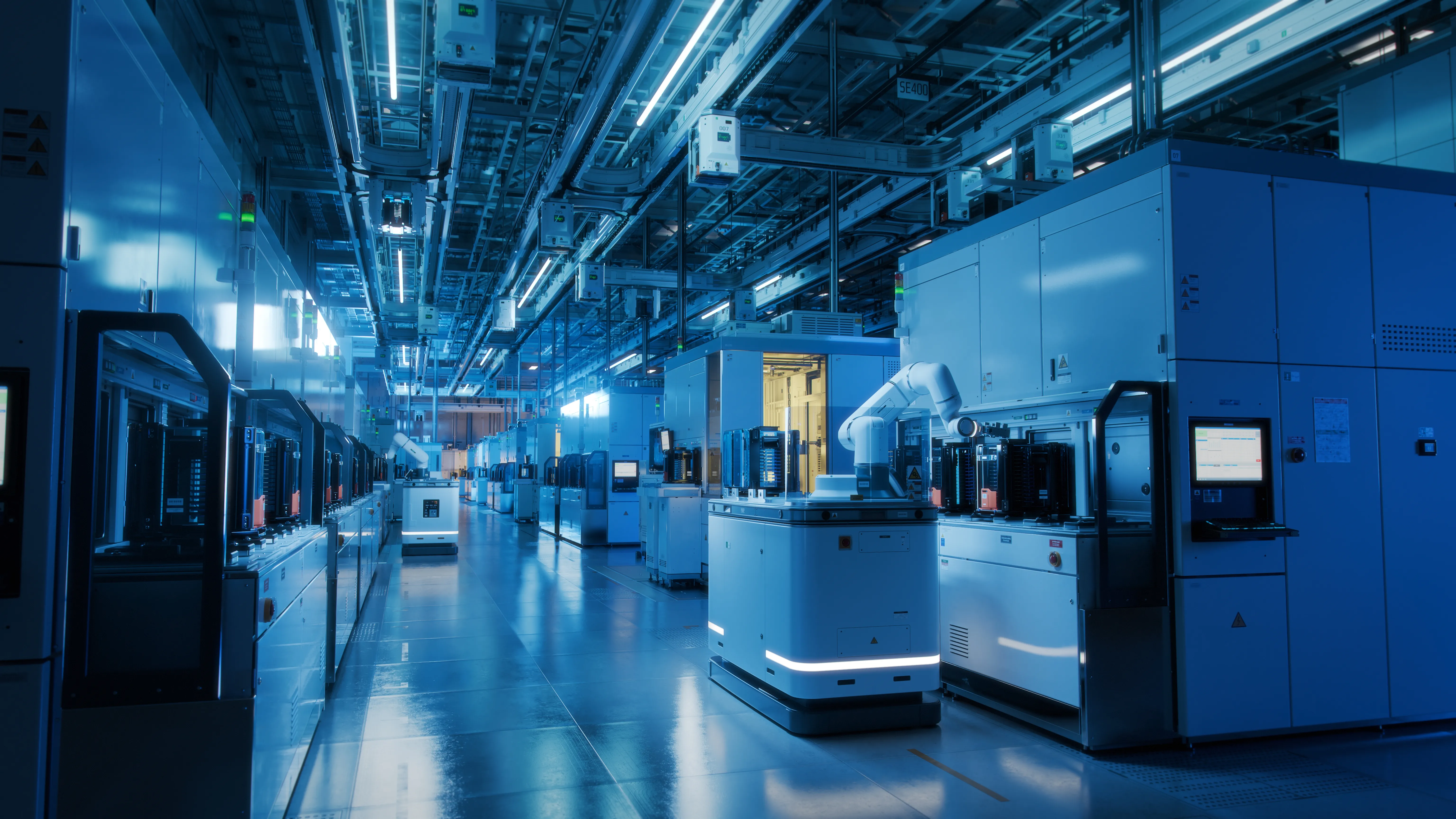
The SEMI Smart Manufacturing Initiative collaboratively crafted this whitepaper with industry members to offer insights from a recent workshop, presenting a comprehensive view of Digital Twin technology in semiconductor manufacturing for achieving AI-driven autonomous factories, covering industry definitions, taxonomy descriptions, and challenges in development and deployment.

Smart Manufacturing White Paper English
The Rising Stars: 20 Under 30 blog series celebrates the brightest young leaders shaping the future of the semiconductor industry. These exceptional individuals have earned the SEMI Europe 20 Under 30 Award for making a remarkable impact across the supply chain—whether in engineering, sales, marketing, or R D. Nominations for the 2026 20 Under 30 Award are now open, providing the opportunity to recognize and honor the next wave of industry trailblazers.The series spotlights these rising stars for their career achievements, commitment to innovation, leadership skills, and dedication to driving both business success and community growth.Follow their inspiring journeys and discover how they are thriving and paving the way for future generations in the semiconductor world.Meet Pascal Fasel, Project Manager Engineering at Comet X-rayPascal Fasel’s career in semiconductors has developed steadily through hands-on experience and continuous learning. Starting with an apprenticeship in 2012, he built his foundation across design, process, and project roles, gaining a practical understanding of how technologies move from concept to production.Over time, he discovered a strong interest in solving real-world problems and delivering reliable engineering solutions. Today, as Project Manager Engineering at Comet X-ray, Fasel focuses on guiding projects through complexity while balancing speed, precision, and quality in a fast-evolving industry. SEMI: What inspired you to join the semiconductor industry? Fasel: I did not have a single defining moment. I joined through an apprenticeship in 2012 and discovered semiconductors gradually. As my responsibilities grew, I realized that I enjoy solving problems and turning ideas into reliable solutions. Over the past three years, I have mainly worked on semiconductor projects, which confirmed this interest. I am motivated by the fast pace, the need for precision and quality, and the impact of bringing new technology into production. It is this combination that keeps me engaged.SEMI: How did your early experiences and education shape your career path?Fasel: My apprenticeship taught me hands-on skills and the importance of quality and safety. Working across design, process, and project roles helped me understand how systems fit together and where problems arise. I am currently studying industrial engineering part-time while working. My studies and work reinforce each other, with theory supporting practice and projects testing what I learn. These experiences keep me focused on preparing technology for production.SEMI: Can you share a professional accomplishment you’re most proud of, and explain why it’s significant to you?Fasel: The accomplishment that matters most to me is my steady growth at Comet. Since joining in 2012, I have worked across design, process, and project roles. Staying for over a decade has been less about titles and more about trust, learning, and supporting colleagues when challenges arise. This is important to me because it reflects consistency and shared responsibility. It has allowed me to contribute to projects from idea to production in a reliable way.SEMI: As a young professional in the industry, what is your greatest challenge? Fasel: My greatest challenge is balancing speed with quality in a changing environment while ensuring smooth handovers to production. Specifications can change, results can be unexpected, and timelines can shift. To manage this, I focus on learning quickly without cutting corners. I make changes small and reversible, identify risks early, and seek feedback regularly. The goal is to learn efficiently and reduce surprises. SEMI: What advice would you give to younger generations aspiring to make an impact in this industry?Fasel: Stay curious and build a habit of learning every day. You will not master everything at once. Projects move quickly, so remain flexible and start with small steps. Gain experience early through internships or student projects. Apply what you learn in practice. Ask clear questions, listen carefully, and stay open to different perspectives. Share credit when things go well and take responsibility when they do not. Be patient. Steady progress is more effective than big jumps. Focus on quality and safety, even under pressure, and build trust through consistency.SEMI: How do you envision future work environments?Fasel: I believe workplaces will become more flexible and people-focused. Clear goals, open communication, and early feedback will be essential. Collaboration will be hybrid, with time in the office used when it adds value. Teams will focus more on outcomes rather than hours, working in small, manageable steps to reduce risk and stay aligned.SEMI: What impact has the 20 Under 30 Award had on your career? Fasel: I am grateful for the recognition. It has not changed my daily work, but it has created opportunities to connect with others, learn from peers, and share experiences. It also provides a platform to encourage students and early-career professionals to explore this industry. For me, it is a reminder to stay consistent and continue supporting others.Following 20 Under 30 JourneysPascal Fasel’s story reflects the value of persistence, practical experience, and continuous improvement. His work highlights how steady progress and collaboration contribute to delivering reliable semiconductor solutions.The Rising Stars: 20 Under 30 blog series celebrates the exceptional talent and leadership driving the future of the semiconductor industry. Each of the young innovators honored is excelling in their respective fields while shaping the landscape of technology and business with their visionary approaches and dedication. Their stories exemplify the remarkable achievements and unwavering commitment that define the next generation of industry leaders. The series is intended to inspire and motivate future professionals to pursue their passions and embrace the opportunities within this dynamic industry. Stay tuned for more stories of rising stars who are paving the way for continued growth and innovation in the semiconductor world.Learn more about the SEMI Europe 20 Under 30 Award and the recipients honored at SEMICON Europa. If this is of interest and you would like to explore further workforce related topics, we invite you to learn more about ChipQuest. SEMI ContactJames Lam, Business Development ManagerEmail: [email protected]
Read More
The semiconductor industry is hitting a structural inflection point: explosive AI‑driven demand, rapidly rising manufacturing complexity, and stringent sustainability expectations are converging at once. In this context, edge AI deployed directly on tools, sensors, and local controllers, is shifting from experimental to essential, particularly in fabs where milliseconds matter. SEMI’s timely workshop, Smarter Sensors, Smarter Fabs: AI at the Edge in Semiconductor Manufacturing, taking place March 18–19, 2026 in Milpitas, CA, will address this important topic.From sparse sensing to dense instrumentationTwo decades ago, most process tools relied on dozens of sensors per chamber. Today, leading etch, deposition, CMP, and lithography systems routinely integrate hundreds of sensing channels spanning pressure, flow, RF power, optical endpoint, vibration, and chemistry. At 3 nm and 2 nm, process windows are so tight that yield hinges on multivariate understanding of chamber conditions and tool state rather than a few independent alarms. Sensor proliferation has turned fabs into rich data environments—but also exposed the limits of traditional, centrally managed control.Why edge AI is displacing cloud‑only controlConventional architectures push heavy analytics to centralized servers or the cloud, with supervisory systems periodically updating recipes, setpoints, or dispatch rules. Across manufacturing, measured cloud round‑trip times commonly range from 800 to 2,400 ms, whereas edge systems co-located with equipment can respond in 15–45 ms, roughly 50–160× faster. For safety‑ and yield‑critical loops in semiconductor manufacturing, that latency gap is often unacceptable.At the same time, new generations of low‑power neural processing units (NPUs) and edge accelerators deliver tens of trillions of operations per second (TOPS) at single‑digit watt budgets, making always‑on inference viable inside tools, cameras, and controllers. The result is a decisive move toward edge‑native architectures: models execute where data is produced, while cloud resources are reserved for retraining and fleet‑wide learning.Edge AI on the line: control, inspection, and maintenanceIn process control, edge AI is enabling a shift from univariate threshold checks to multivariate models that understand the joint dynamics of sensor streams. Platforms today embed deep‑learning and statistical models directly at or near the tool, performing real‑time endpoint prediction and anomaly detection from high‑dimensional time series. Similar approaches are emerging in lithography and CMP, where local inference helps keep focus, overlay, and removal rate within spec before wafers drift out of control.Inspection and logistics are undergoing a similar transformation. Vision systems with embedded NPUs classify defects at line speed, often above 100 parts per minute, eliminating the need to ship large image volumes to a central cluster. Robots and autonomous mobile robots (AMRs) use local intelligence for short‑horizon planning and collision avoidance, while higher‑level systems focus on global scheduling and optimization.Predictive maintenance is one of the most mature applications: vibration, acoustic, temperature, and pressure data are analyzed locally to detect anomaly signatures hours or days before conventional thresholds trip. Reported benefits include reductions in unplanned downtime, longer component life, and lower maintenance costs when these models are integrated into manufacturing execution systems (MES) and maintenance workflows.Digital twins and agentic AI on top of edge dataDigital twins build on this sensing and edge‑analytics foundation. By maintaining virtual, live‑updated models of tools, lines, and entire fabs, they enable scenario testing, debottlenecking, and root‑cause analysis without putting WIP at risk. Vendors and early adopters report that such twins can shorten process‑node ramps and facility bring‑up by enabling thousands of “what‑if” experiments before physical changes are made.​Agentic AI is now emerging as the orchestration layer above these twins. In semiconductor case studies, agents connected to MES, advanced process control (APC), and planning systems have delivered double‑digit improvements in throughput, cycle time, and tool utilization by autonomously adjusting routing, batch sizes, and scheduling in response to live fab conditions. Other agents mine unstructured engineering notes and fault reports to accelerate root‑cause analysis, turning hard‑won lessons into repeatable, codified behavior.Sustainability as a first‑class requirementSustainability pressures are reinforcing this stack. Semiconductor manufacturing is energy‑ and resource‑intensive, and regulators and customers alike are demanding more transparency and improvement. Edge‑connected monitoring of energy, utilities, and emissions has already helped some fabs cut energy‑related costs by around 20 percent through tighter control of HVAC, process gases, and idle modes. Research initiatives such as imec’s Sustainable Semiconductor Technologies and Systems (SSTS) program are using virtual fab methods and detailed life‑cycle assessment to guide process and equipment choices for lower environmental impact.Strategic takeaways and where to learn moreThe trajectory is clear: fabs that combine dense sensing, edge AI, digital twins, and agentic AI are building toward continuously learning, self‑optimizing operations. Architectures will need to be edge‑first rather than cloud‑only. Simply adding sensors without local intelligence will not deliver competitive advantage, and environmental KPIs are likely to be optimized with the same rigor as yield and cycle time.For practitioners who want to translate these trends into roadmaps, the Smarter Sensors, Smarter Fabs: AI at the Edge in Semiconductor Manufacturing” workshop (March 18–19, 2026, Milpitas, CA) spearheaded by the SEMI Manufacturing Coalitions* will bring together experts in sensing, edge architectures, digital twins, and agentic AI to share concrete deployments and architectures tailored to semiconductor fabs.*The SEMI Manufacturing Coalitions include Smart Manufacturing, Fab Owners Alliance (FOA) MEMS and Sensors Industry Group (MSIG), Advanced Packaging Heterogenous Integration (APHI) and Semiconductor Components, Instruments, and Subsystems (SCIS). Anshu Bahadur is Senior Program Manager, Technology Communities at SEMI. Mark da Silva is Senior Director, Manufacturing Coalitions at SEMI.
Read More
At SEMICON Europa 2025, the Executive Forum programs brought together experts from across the semiconductor value chain to address two critical challenges shaping the industry’s future in Europe: the transformation of the automotive sector and the pursuit of smarter, more competitive manufacturing.Smart Mobility in a Changing MarketKnut Krümmel, Senior Partner Automotive at Porsche Consulting, set the tone with a stark question, “Are we facing a Detroit scenario in Europe, especially in Germany?” – a reference to the decline since the 1990s of the famous “Motor City.” He pointed out that all three of Germany’s giant OEMs, Volkswagen, Mercedes-Benz and BMW, are rapidly losing market share in China in the face of a destructive price war, and have suffered large declines in reported earnings. Krümmel outlined four strategic imperatives for Europe’s auto industry: reduce complexity and increase standardization, become software-defined, design regulation that supports innovation, and build stronger partnerships across the ecosystem. He emphasized, “A new mindset is needed—people need to be hungry to win and prepared to suffer in pursuit of victory.”Knut Krümmel, Senior Partner Automotive, Porsche Consulting GmbHAndreas Aal, Head of Semiconductor Strategy at Volkswagen AG and Chair of Europe at SEMI Smart Mobility Global Automotive Advisory Council (GAAC), introduced a proactive approach to redefine the market. He shared Volkswagen’s vision for mobility-as-a-service, exemplified by its roboshuttle pilot in Hamburg. “It is very difficult for a traditional OEM to go into the full digital services world. But this is what we want to do,” said Aal.Andreas Aal, Semiconductor Strategy Volkswagen AG and Chair of Europe GAAC, VolkswagenJan-Philipp Gerhmann, Vice President of Marketing and Strategy for Automotive at NXP Semiconductors, added that the traditional value chain is being upended. The industry is shifting from a hierarchical supply chain to vertical integration, with companies like Tesla designing their own chips. Gehrmann introduced NXP’s CoreRide platform, a modular “skateboard” architecture enabling plug-and-play Advanced Driver Assistance Systems (ADAS) and infotainment features for future vehicles.Jan-Philipp Gehrmann, Vice President of Marketing Strategy, NXPA perspective on the future of semiconductors in autonomous vehicles was provided by Dieter Hoffend, Business Director for Automotive at imec: “For autonomous vehicles, you need a higher-end compute capability, which needs a transition to smaller nodes – and that is very costly. In fact, semiconductor companies will not want to commit volume to automotive customers for their most expensive leading-edge ICs. This means that a chiplet architecture will be the most cost-effective approach for vehicles, and will provide the greatest supply chain resilience. To support this, imec’s vision is of an open chiplet marketplace of heterogeneous chiplets which are interoperable.”Dieter Hoffend, Business Director Automotive Sector, imecAchieving End-to-end Manufacturing ExcellenceThe Executive Forum then shifted to a discussion of smart semiconductor manufacturing. Giovanni Notarnicola, Partner at Porsche Consulting, highlighted the untapped potential of AI in fabs. “AI requires massive amounts of data—but fabs often don’t own or control their data. And second, AI talent doesn’t typically reside in semiconductor companies,” said Notarnicola. His recommendation: “AI is not an IT issue—it’s a cross-functional technology. Isolating AI in the IT department is an old-fashioned view which will deter AI talent from joining the industry.”And Notarnicola encouraged the industry to leverage the new white paper produced by SEMI End-to-End Smart Manufacturing Group, which provides an in-depth report on the application of AI in semiconductor fabrication. Giovanni Notarnicola, Partner, Porsche ConsultingOliver Aubel, Corporate Lead for Automotive Solutions at GlobalFoundries, echoed the opportunity. “We have 1 billion sensors in a fab, but 30% of the signals are statistical noise. AI could help us make better sense of the data.”Oliver Aubel, Corporate Lead for Automotive Solutions at GlobalFoundriesA session on smart manufacturing brought to light other proven methods for improving the performance of fabs. Dr. Holland Smith, Director of Data Science at INFICON, described fab control technology that INFICON had helped STMicroelectronics to deploy. As Thomas Gimmig, Director for Industry 4.0 at STMicroelectronics, said, “Our model was a highway control room – a place where a single person controls 220km of road monitored by 400 cameras, and handles one alert every three minutes on average. This is only possible with a huge amount of automation.”Left: Thomas Gimmig, Director for Industry 4.0 at STMicroelectronics; Right: Dr. Holland Smith, Director of Data Science at INFICONAt STMicroelectronics, the new fab control room mimics this model, automating anomaly detection and problem solving. Smith described how the system will not be limited to detecting and handling anomalies which have already occurred. “There is a plan to look ahead at problems which could emerge in future, and to configure it to make proactive suggestions which will prevent anomalies from occurring in the first place,” said Smith. Jamie Potter, co-founder and CEO of Flexciton, showcased how intelligent scheduling tools based on real-time fab capacity are transforming operations. “In the modern fab decisions must be made more frequently, with more intelligence and with fewer people. And that is why fabs need to be made more autonomous,” said Potter.Jamie Potter, CEO Cofounder, Flexciton Ltd“Our tool is based on a dynamic capacity model of the fab, so WIP optimization is based on knowledge of what the fab can actually do now, rather than – as is normally the case in fabs today – on an abstract algorithm which is derived from operational results observed in the past.” Potter said. Robert Wallace, Solutions Architect at Seagate, which has deployed the Flexciton technology, confirmed the impact: “We increased throughput without increasing cycle times, and saw a 30% drop in deviations from forecast completion times.” Robert Wallace, Solutions Architect at SeagateAntoine Amade, President (EMEA) of Entegris, emphasized the importance of benchmarking to guide performance improvements: “We have a robust library of fab case studies. These benchmarks can become the foundation for best practices.” Antoine Amade, President (EMEA) of EntegrisRegulatory Burdens and Regional Challenges In a panel session, the discussion turned to the issues that European semiconductor manufacturing faces in particular. Herbert Blaschitz, Executive Vice President of Advanced Technology Facilities at Exyte, put a strong emphasis on the drag that European regulation imposes on the construction of new fabrication plants: “There is three times more paperwork to complete in Europe than in Asia.” Blaschitz made the contrast with Taiwan, “where they have standard codes of regulation specifically for a wafer fab. In Europe, we have regulations for skyscrapers, we have regulations for building family homes. But we have nothing for wafer fabs.”It could be worse for companies building all new fabs. According to Stephen Rothrock, President and CEO of ATREG, “We are affected by permits and politics most of all when trying to push through the repurposing of fabs.”From Left to Right: Mark Puttock, Sr. Director - Technology and Innovation, Entegris; Giovanni Notarnicola, Partner, Porsche Consulting; Stephen Rothrock, President/CEO, ATREG; Jean-René Lèquepeys, Deputy Director and Chief Technology Officer, CEA-Leti; Herbert Blaschitz, Executive VP of Advanced Technology Facilities, Exyte; Oliver Aubel, Corporate Lead Automotive Solutions, GlobalFoundriesSustainable Manufacturing Practices: A Source of Competitive Advantage?The forum ended with a debate on the value of and problems with Europe’s commitment to sustainability. As Mark Puttock, Senior Director for Technology and Innovation at Entegris, acknowledged concerns that sustainability practices could raise costs and reduce process efficiency. But Jean-René Lèquepeys, Deputy Director and Chief Technology Officer at CEA-Leti, countered: “sustainability can be a competitive advantage. For instance, the industry is under pressure to eliminate PFAS from its processes. CEA-Leti is working on this problem, and the whole world is looking for a solution.”The event concluded with a moment of celebration: Ilya Zabelinsky, Co-founder of the International Subfab Research Labs (ISRL), won a diamond prize sponsored by Nanores Lab,Left: Jakub GawczyńskiJakub Gawczyński, Head of Nanores Lab; Right: Ilya Zabelinsky, Co-founder of the International Subfab Research Labs (ISRL)On behalf of SEMI, we extend our sincere gratitude to the speakers, sponsors, and participants who contributed their expertise and vision to the programs at SEMICON Europa 2025.SEMI ContactAna Bernardo, Senior Manager of Technology Programs SalesEmail: [email protected]
Read More
The Rising Stars: 20 Under 30 blog series celebrates the brightest young leaders shaping the future of the semiconductor industry. These exceptional individuals have earned the SEMI Europe 20 Under 30 Award for making a remarkable impact across the supply chain—whether in engineering, sales, marketing, or R D. Nominations for the 2025 20 Under 30 Award are now open, providing the opportunity to recognize and honor the next wave of industry trailblazers.The series spotlights these rising stars for their career achievements, commitment to innovation, leadership skills, and dedication to driving both business success and community growth.Follow their inspiring journeys and discover how they are thriving and paving the way for future generations in the semiconductor world.Meet Anne-Mary Yeboah, Technology Manager at SoitecWith a background in materials science and a strong interest in technology, Anne-Mary Yeboah has built a career that connects the worlds of engineering and management. After earning her degree in engineering, she deepened her understanding of business through a Specialized Master’s in Management—an experience that broadened her perspective and prepared her for the challenges of a global, fast-moving industry.Today, as Technology Manager at Soitec, Yeboah leads projects that contribute to the next generation of semiconductor innovations. Her journey reflects a balance of technical curiosity, leadership growth, and a belief in the power of inclusion. In this interview, she shares her thoughts on career development, the importance of diversity, and how young professionals can find their voice in a rapidly evolving industry.SEMI: What inspired you to join the semiconductor industry? Yeboah: I’ve always been fascinated by technology, and semiconductors are at the core of innovation today. They are everywhere, from smartphones to electric vehicles, and being part of this field means contributing directly to the technologies shaping our lives and future.SEMI: How did your early experiences and education shape your career path?Yeboah: My engineering studies led me to specialize in materials science, which naturally included semiconductors. Later, I decided to expand my knowledge by pursuing a Specialized Master’s in Management. This combination of technical and business perspectives shaped my career path and ultimately brought me to Soitec, where I now connect both worlds as a Technology Manager.SEMI: Can you share a professional accomplishment you’re most proud of, and explain why it’s significant to you?Yeboah: I’m especially proud of starting my career directly as a Technology Manager. This role has allowed me to contribute to complex, strategic projects and collaborate with teams across functions. Working on products that will drive future innovations is deeply fulfilling and gives meaning to my work every day.SEMI: As a young professional in the industry, what is your greatest challenge? Yeboah: One of the biggest challenges has been finding my voice in a highly experienced environment. It can be intimidating at first, but I’ve learned to turn it into an opportunity to ask questions, learn quickly, and build confidence in my contributions. It has pushed me to develop a broad skill set and become an effective collaborator across teams.SEMI: What advice would you give to younger generations aspiring to make an impact in this industry?Yeboah: Dare to step forward and don’t create your own limits. Ask questions, even when you’re surrounded by experts, curiosity is a strength. Also, be patient. Building credibility and seeing your impact takes time, but each experience helps you grow and move closer to your goals.SEMI: How do you envision future work environments?Yeboah: I see the workplaces of the future as more innovative, inclusive, and collaborative. Diversity should be central, everyone should feel that their voice and perspective matter. At Soitec, initiatives like Women@Soitec are great examples of how gender equality and inclusion can empower people to thrive. I also believe technology and flexibility will continue to reshape how we work, helping us achieve both high performance and balance.SEMI: What impact has the 20 Under 30 Award had on your career? Yeboah: Receiving the 20 Under 30 Award has been a true honor and a wonderful source of motivation. It gave me a moment to reflect on how far I’ve come and to feel proud of my journey. The recognition has boosted my confidence, increased my visibility, and encouraged me to continue pushing forward in my career.Following 20 Under 30 JourneysAnne-Mary Yeboah’s story highlights the determination and adaptability driving today’s new generation of semiconductor professionals. Her ability to bridge science and management reflects the diverse skill sets shaping the industry’s future.The Rising Stars: 20 Under 30 blog series celebrates the exceptional talent and leadership driving the future of the semiconductor industry. Each of the young innovators honored is excelling in their respective fields while shaping the landscape of technology and business with their visionary approaches and dedication. Their stories exemplify the remarkable achievements and unwavering commitment that define the next generation of industry leaders. The series is intended to inspire and motivate future professionals to pursue their passions and embrace the opportunities within this dynamic industry. Stay tuned for more stories of rising stars who are paving the way for continued growth and innovation in the semiconductor world.Learn more about the SEMI Europe 20 Under 30 Award and the recipients honored at SEMICON Europa. SEMI ContactJames Lam, Business Development ManagerEmail: [email protected]
Read More
The Rising Stars: 20 Under 30 blog series celebrates the brightest young leaders shaping the future of the semiconductor industry. These exceptional individuals have earned the SEMI Europe 20 Under 30 Award for making a remarkable impact across the supply chain—whether in engineering, sales, marketing, or R D. Nominations for the 2025 20 Under 30 Award are now open, providing the opportunity to recognize and honor the next wave of industry trailblazers.The series spotlights these rising stars for their career achievements, commitment to innovation, leadership skills, and dedication to driving both business success and community growth.Follow their inspiring journeys and discover how they are thriving and paving the way for future generations in the semiconductor world.Meet Eloise Bond, Senior Etch Process Engineer at KLA Corporation (SPTS Division)Eloise Bond studied Physics at Swansea University before joining KLA in 2019 as an Etch Process Engineer. Since then, she has worked on cutting-edge semiconductor applications while actively promoting STEM through local outreach programs like Generation Tech.A proud recipient of the SEMI Europe 20 Under 30 Award, Bond shares how the recognition boosted her confidence and expanded her network, enabling her to take on new challenges. In her interview, she reflects on overcoming imposter syndrome, the value of flexible work, and the unexpected opportunities that shaped her career. Outside of work, Bond enjoys camping and bouldering.SEMI: What inspired you to join the semiconductor industry? Bond: I’ve always had a passion for science, so pursuing a career in a related field was natural. However, I wasn’t aware of the semiconductor industry until I began studying Physics at Swansea University, which has strong research ties with local semiconductor companies like KLA. Now that I am in the industry, I enjoy the hands-on aspects of my job. I find working with different materials and equipment is more engaging to me than an office-based job. SEMI: How did your early experiences and education shape your career path?Bond: STEM activities during my childhood and visits to museums with my parents sparked my interest in science and the physical world. That curiosity lead me to study physics at Swansea University, which ultimately paved the way to my current role at KLA. As I mentioned earlier, a career in semiconductors wasn’t really a conscious choice until relatively late in my education; I simply followed my passion for science. Today, I’m involved in many of the STEM outreach programs at KLA, helping to promote the semiconductor industry to young children so they can discover the same opportunities that I was fortunate to have had exposure to earlier in my life.SEMI: Can you share a professional accomplishment you’re most proud of, and explain why it’s significant to you?Bond: One accomplishment I’m particularly proud of is building strong customer relationships with a volume production fab in Korea. It was my first experience with direct customer interactions, which felt quite daunting at the time. I was invited to support a tool installation on-site, which allowed me to travel the furthest from the UK I had ever gone. Seeing firsthand how our tools fit into the wider industry gave me valuable context for my day-to-day responsibilities and made my work feel even more impactful. SEMI: As a young professional in the industry, what is your greatest challenge? Bond: Imposter syndrome has been a significant challenge for me. I often find myself in meetings with more senior colleagues and fear I am not performing well enough. However, over time, I have learned that my input is valid and that having multiple perspectives often leads to better outcomes.SEMI: What advice would you give to younger generations aspiring to make an impact in this industry?Bond: To make a difference, you first need to be part of the industry, just getting involved puts you in the room where conversations and decisions happen that you might not otherwise be exposed to.If an opportunity comes your way, take it. I entered this industry due to an opportunity presented to me at the end of my university career. KLA was my first real interview, and I honestly thought my chances were slim. I approached it as a ‘trial run’ and five years later, I’m still here. SEMI: How do you envision future work environments?Bond: I envision a new generation of management that places greater value on work-life balance. In many industries, senior management seem to have a relatively poor work-life balance, such as constantly doing business in the same way they’ve done for the past 40+ years – with constant business travel, working on holidays and long hours in the office. There is still an expectation for younger, ambitious employees to emulate this corporate culture, which creates barriers for those with caregiving responsibilities or other important commitments outside work. I believe a younger, more vocal generation of managers will drive positive changes in how we work. We will see more adoption of fully flexible working and 4-day weeks – happy employees lead to better work outcomes. I also think the technological advances which enabled the rapid switch to “working from home” during the COVID pandemic have permanently reshaped what is possible in terms of flexibly and efficiently.SEMI: What impact has the 20 Under 30 Award had on your career? Bond: This award has given me greater confidence to step outside of my comfort zone. It has also allowed me to increase my network to include colleagues I would have no reason to speak to previously. As a result, I have gained broader knowledge of how KLA operates as a whole and have been able to initiate small cross departmental projects I would not have been possible to before. Following 20 Under 30 JourneysEloise Bond’s journey highlights the passion, resilience, and forward-thinking mindset that characterize today’s emerging leaders in semiconductors. Her dedication to both technical excellence and community engagement showcases how rising stars are not only advancing the industry but also inspiring the next generation.The Rising Stars: 20 Under 30 blog series celebrates the exceptional talent and leadership driving the future of the semiconductor industry. Each of the young innovators honored is excelling in their respective fields while shaping the landscape of technology and business with their visionary approaches and dedication. Their stories exemplify the remarkable achievements and unwavering commitment that define the next generation of industry leaders. The series is intended to inspire and motivate future professionals to pursue their passions and embrace the opportunities within this dynamic industry. Stay tuned for more stories of rising stars who are paving the way for continued growth and innovation in the semiconductor world.Learn more about the SEMI Europe 20 Under 30 Award and the recipients honored at SEMICON Europa. SEMI ContactMaria Daniela Perez, Communications ManagerEmail: [email protected]
Read More
Silicon carbide (SiC) has become a cornerstone of next-generation power electronics, driving advancements in electric vehicles, renewable energy, and industrial applications. After several years of rapid capacity expansion, the SiC industry is now entering a new phase focused on optimization, quality, and long-term scalability.This transition reflects a broader realignment across the global semiconductor ecosystem. As new fabs come online and supply chains mature, the industry is prioritizing stability, cost efficiency, and technical excellence over sheer capacity growth. SiC has moved from being a niche technology to a critical enabler of the energy transition, and this maturity demands not only investment in tools and materials, but also in process knowledge, cross-industry standards, and long-term partnerships that can sustain innovation at scale.To understand how this shift is unfolding, SEMI Europe spoke with Dr. Mark Puttock, Senior Director, Technology and Innovation at Entegris. Puttock shared his perspective on the industry’s evolution and how strategic collaboration and process innovation are shaping the next chapter of SiC manufacturing.From Ramp-Up to RefinementThe early growth of SiC manufacturing was driven by surging demand for high-efficiency power devices, particularly in electric vehicles. According to Puttock, that expansion period has given way to a new focus on yield, uniformity, and process control.The industry is entering a stage of maturity where success depends on optimization rather than scale alone. Improving consistency across crystal growth, wafer, and device fabrication is becoming just as important as adding capacity. This refinement phase calls for closer integration between materials science and manufacturing technology to ensure reliability and cost efficiency.A Focus on Process and Materials InnovationAs SiC moves toward high-volume production, challenges related to contamination control, defectivity, and wafer uniformity are taking center stage. Puttock noted that addressing these issues requires collaboration between materials suppliers, equipment manufacturers, and device makers.Efforts across the industry are converging on similar goals: enhancing purity, improving process repeatability, and developing new methods to enable larger wafer formats. Moving from 6-inch to 8-inch SiC wafers, for example, is widely recognized as a key step toward higher throughput and cost efficiency. Puttock emphasized that innovation in materials science and manufacturing technology must go hand in hand to support this scaling trend.Insights from Cross-Industry CollaborationA recent Entegris blog post featuring insights from Volkswagen Group Components and Porsche Consulting explores how SiC adoption is reshaping manufacturing strategies beyond the semiconductor industry. The post also highlights the strategy paper developed by Porsche Consulting in collaboration with Entegris. This joint effort demonstrates the value of aligning semiconductor-grade precision with automotive manufacturing demands. By sharing perspectives across industries, partners can accelerate best-practice adoption and strengthen the overall ecosystem for wide-bandgap technologies.Building a Sustainable FutureSustainability remains an integral part of this optimization phase. SiC devices themselves enable energy efficiency in end applications, but the way they are manufactured is equally important. Optimizing material use, recycling process consumables, and improving chemical delivery efficiency all contribute to a smaller environmental footprint. As production scales, attention to both performance and sustainability will be key to long-term success.Looking ForwardThe transition from expansion to optimization marks a pivotal moment for SiC manufacturing. Industry focus is shifting from building capacity to mastering control, quality, and resource efficiency. Puttock sees the future of SiC as one shaped by deeper digital integration, data-driven process development, and continued collaboration across disciplines. These advancements will help enable more consistent, sustainable, and cost-effective production—laying the foundation for the next generation of high-performance power devices.At the same time, Entegris continues to invest in materials science, contamination control, and advanced process technologies that help its customers overcome the complex challenges of SiC manufacturing. By combining technical expertise with a collaborative approach, the company plays an active role in supporting the industry’s transition toward more efficient and sustainable production.James Lam is Business Development Manager at SEMI Europe.
Read More
Atomic layer deposition (ALD) and atomic layer etching (ALE) are transforming the way semiconductors are built—layer by layer, atom by atom. These atomic-scale processes are essential to scaling future transistors, improving memory, and enabling next-generation device architectures.SEMI spoke with Sergei Ivanov, Business Technology Director of Metallics R D and Balaji Kannan, Business Technology Director of Dielectrics R D and from Merck KGaA, Darmstadt, Germany to learn about their latest material innovations. At the company’s Electronics business, materials scientists and process engineers are advancing atomic-scale engineering to address some of the semiconductor industry’s toughest challenges. From novel deposition chemistries to next-generation etch techniques, their work is helping to enable future logic, memory, and specialty devices.Pushing the Boundaries of ALD Precursor ChemistryAtomic Layer Deposition (ALD) remains a cornerstone technology for scaling transistors and enabling new architectures. Materials scientists at Merck KGaA, Darmstadt, Germany are exploring novel precursors that enhance film quality, streamline processes, and expand the operational window for complex structures:One area of focus is next-generation hafnium and zirconium precursors. “These advanced high-k dielectrics offer better thermal stability, improved step coverage, and reduced impurities while achieving higher k-values,” Sergei Ivanov explained. “Such attributes are essential for logic and memory devices that demand reliable dielectric performance with minimal defect density.”Another important development is area selective deposition (ASD). Merck KGaA, Darmstadt, Germany’s small-molecule inhibitor solutions reduce the need for advanced patterning in narrow dimensions and 3D geometries, enabling cost-effective and simpler integration for leading-edge nodes. Their selective co-reactants platform leverages digitalization techniques including multivariate analysis, digital twin technology, and machine learning to accelerate process development for critical ASD applications. This approach facilitated industry-first adoption of ASD in high volume manufacturing and enables an ever-expanding toolbox of OEM processes for ASD of high-k, Ti, Mo, Si and other thin films.Merck KGaA, Darmstadt, Germany is also broadening the scope of ALD chemistries across the periodic table. “As our customers encounter new technical challenges, we continue to expand our R D scope across new elements and ligands. Examples include europium, lanthanum, scandium, and cerium dopants with improved electrical properties, niobium and vanadium precursors for deposition of nitride and oxide films with reduced impurities and improved ALD performance, and high-performance nickel MILC solutions are finding their way out of our labs and into customer roadmaps at an ever-accelerating pace,” said Sergei Ivanov.The company’s role in molybdenum chemistry is another example. Merck KGaA, Darmstadt, Germany is a key producer of molybdenum precursors including MoO2Cl2 with industry-leading quality, density, and container utilization. The company offers MoCl5 with advanced trace impurity control paired with innovative container technology. The company’s next-generation organic metallic molybdenum precursors incorporate novel ligands that contribute to critical gains in device performance.Merck KGaA, Darmstadt, Germany’s work with organosilane precursors is also opening new possibilities. “For gate-all-around (GAA) transistor technology, precursors incorporating novel bonding structures enable highly conformal dielectric films with excellent electrical and physical properties, even in complex 3D geometries. At the same time, organosilane chemistries designed to increase silicon incorporation during deposition are supporting high-growth-rate oxides for gapfill applications, delivering the thick films required with greater throughput,” said Balaji Kannan. “Together, these innovations highlight how tailored precursor design can address both scaling challenges and manufacturability in next-generation devices.” Driving Selective and Sustainable Atomic Layer Etching (ALE)“Precision in etching is as critical as deposition. Our innovations in ALE are designed to provide ultra-selective, low-damage material removal, which is increasingly vital as device geometries become finer and more complex,” Sergei Ivanov shared. One example is metal-free ligand exchange ALE for high-k materials, where Merck KGaA, Darmstadt, Germany’s research into etching HfO₂, ZrO₂, and HfZrO₄ showcases a novel metal-free approach. This technique enables accurate and damage-minimized etching of high-k dielectrics, which is essential for integrating advanced transistors and memory stacks.These advancements address industry-wide concerns regarding pattern fidelity, material selectivity, and plasma-induced damage, ensuring greater process control and extending the lifetimes of devices.Looking AheadMerck KGaA, Darmstadt, Germany’s strategic commitment to semiconductor innovation includes ongoing R D efforts that reflect the vision of its Electronics business: providing material-centric solutions to the industry’s most complex integration and performance challenges. Whether advancing front-end device scaling or developing breakthrough materials for emerging applications, the Electronics business of Merck KGaA, Darmstadt, Germany is committed to shaping the materials roadmap for a more connected, intelligent, and efficient world.James Lam is Business Development Manager at SEMI Europe.
Read More