downloadGroupGroupnoun_press release_995423_000000 copyGroupnoun_Feed_96767_000000Group 19noun_pictures_1817522_000000Member company iconResource item iconStore item iconGroup 19Group 19noun_Photo_2085192_000000 Copynoun_presentation_2096081_000000Group 19Group Copy 7noun_webinar_692730_000000Path
Skip to main content
Default Banner Image

SEMICON West

This year’s SEMICON West has new dates, a new location in a new city and a new addition to the program—design! “The Convergence of Semiconductor Manufacturing and Design” will highlight the collaboration between semiconductor manufacturers and chip design teams to bring advanced systems to market. The three-hour session during SEMICON West will be held Tuesday, October 7, from 1-4 p.m. at the Phoenix Convention Center in Phoenix, Arizona.Five 20-minute presentations will describe successful collaborations and address challenges and opportunities about design and manufacturing security, long-term reliability, system performance issues, and modeling and verification that encompass the entire system. Attendees can expect to learn about the key drivers behind the need for collaboration that range from heterogeneous integration to advanced packaging technologies and applications such as automotive and medical.Session moderators are Ming Zhang, PhD, Vice President of Fabless Solutions of PDF Solutions, and me. “As design and manufacturing complexity continues to grow, driven by applications like AI, it is becoming increasingly difficult to account for every manufacturing variation during design and at sign-off or to fully anticipate the entire design space at chip and system levels during manufacturing technology development,” said Zhang. “Achieving tighter integration between design and manufacturing through broader and deeper data and methodology collaboration will be critical to improving predictability, accelerating time to market and enabling the next generation of semiconductor innovation.”It’s within this context that we selected the presenters who include:“Revolutionizing Silicon to Systems Design: Unlocking the Future with 2.5D and 3D Multi-Die Innovations” by Sutirtha Kabir of Synopsys.“Manufacturing to Development to Manufacturing for Circular Collaboration Leveraging AI and Other EDA Advances” with David Kelf from Breker Verification Systems.“Bridging the Silicon Divide: Converging Chip Design and Manufacturing in the Era of High Integration” from Lu Dai at Qualcomm Technologies.“3D and Chiplets Driving Moore’s Law into the Future” with Joe Kwan of Siemens EDA.“Multiphysics Multiscale Challenges and Solutions for 3D Heterogenous Integration” by Sudarshan Mallu from Ansys, part of Synopsys.The program concludes with a panel moderated by Zhang titled “The Convergence of Semiconductor Manufacturing and Design” and features the session presenters.Join us to learn how the semiconductor manufacturing and design communities are collaborating to deliver advanced systems based on chiplets and rapidly emerging packaging technologies including 2.5D and 3D ICs and MCMs. Audience participation will be encouraged.Also of interest to attendees is a SEMICON West keynote from John Kibarian, CEO, President and Co-Founder of PDF Solutions who is also co-chair of SEMI’s ESD Alliance Governing Council. Kibarian will address “Revolutionizing Semiconductor Collaboration: The Emergence of AI-Driven Industry Platforms” during the CEO Summit keynotes on Wednesday, October 8 at 10:20 a.m.SEMICON West 2025 makes its debut in Phoenix, October 7-9 at the Phoenix Convention Center. This milestone event gathers global leaders across the microelectronics supply chain to explore transformative technologies, develop the future workforce and drive strategic collaboration. Moving SEMICON West to Phoenix highlights Arizona as a key hub for innovation and industry growth. Visit the SEMICON West homepage for more details on full program, including “The Convergence of Semiconductor Manufacturing and Design” session, special features, sponsors and exhibits. Registration is open. Robert (Bob) Smith is executive director of the ESD Alliance, a SEMI Technology Community. 
Read More
In Q2, the SEMI International Standards Program made progress on several emerging initiatives. Together, we reached a critical milestone for one of our data standards initiatives with Document 6938C recently passing Technical Committee review in mid-June 2025. Ballot 6938C, which provides guidance on how to identify manufacturing equipment data provided by the equipment supplier that can be used in equipment engineering or analysis applications, is slated to join SEMI E190 and E190.1 in providing industry-enabling data standardization.In addition, we began major revisions to SEMI Standards S2, S8, and S10. These standards govern environmental, health, and safety (EHS) considerations, equipment user fatigue and injury reduction, and equipment risk assessment and evaluation, respectively. In our recently concluded North America Standards Summer 2025 Meetings, the NA EHS Technical Committee Chapter approved a revision ballot to SEMI S10. The ballot (7169) proposed several major revisions to the SEMI S10 Safety Guideline on risk assessment which included changes to references to equipment to objects under consideration. Other changes also included the relocation of the assessment of the risk of harm to property other than the OUC to a Related Information section. Additional details are provided below.We’re eagerly preparing for this year’s SEMICON West event, taking place for the first time ever in Phoenix, Arizona. We are also pleased to announce the return of the SEMI Global Standards Summit taking place Tuesday afternoon, October 7 at SEMICON West. Our inaugural Summit was held last year at SEMICON Japan 2024 last December. The Summit aims to identify standards-critical areas and work towards an industry standardization strategy for the next 3- and 7-year time horizons. This year's Global Standards Summit will feature sessions on Supply Chain Traceability as well as Environmental Sustainability. Similarly, as cybersecurity considerations become more complex, SEMICON West will host a dedicated Cybersecurity Forum from October 7-9 to address today’s most pertinent challenges. More detailed program information will be available soon. Finally, we’re looking forward to our SEMI Standards + Award Ceremony Networking Event at SEMICON West. Following the International Standards Meeting and Standards Summit on Tuesday, October 7, join us for appetizers, drinks, and great conversation from 6-7:30 p.m. In the meantime, learn more about becoming a member of the SEMI International Standards Program.Balloting for Document 6938Document 6938C introduces a new potential standard – Guide for Equipment Edge Data Governance. Under development by the Equipment Edge Data Governance (EEDG) Task Force since 2021, Document 6938C was balloted in Cycle 3-2025 and approved during the Information Control Taiwan Technical Committee (TC) Chapter meeting held on June 12, 2025. It has since received approval by the International Standards Committee Audits and Reviews Subcommittee and is now undergoing final processing for publication by SEMI. As manufacturing equipment offers more accessible data than ever, poor communication, inconsistent expectations, and data security concerns continue to halt or slow factory integration efforts. If passed, this new standard will help organize the information that supports smart manufacturing efforts at the edge. In addition, the EEDG Guide will provide a comprehensive set of best practices to both users and suppliers to increase the value of existing equipment data. Update on Revisions to SEMI S2, S8, and S10 Safety GuidelinesOur 2025 Q1 Standards Watch newsletter announced a significant overhaul for SEMI Standards S2, S8, and S10.S2, SEMI’s standard for performance-based environmental, health, and safety (EHS) considerations for semiconductor manufacturing equipment, is undergoing discussions on redefining safety interlock systems. The S2 task force will issue an informal ballot to the general audience for feedback. The results then will be used to develop a formal letter ballot.First developed in 1995, SEMI Standard S8 works to reduce fatigue and injury by matching equipment to the user’s size, strength, and range of motion. Although this safety standard has been periodically updated since its inception, its last substantial revision was in 2018. The ballot to revise S8 ultimately failed the EH S TC Chapter review at this year’s Winter Meeting. With 214 comments and negatives to consider, the task force is revising the ballot and plans to reissue in Cycle 7 of August 2025.Finally, SEMI Standard S10 is moving through ballot 7169. This standard defines a consistent means of risk estimation that other SEMI Safety Guidelines can invoke. Ballot 7169 will separate facility and building risk assessment to a non-normative portion of the document, ensure EHS risks are separately calculated from commercial object risks, and clarify risk assessment of observed events from risk assessment of foreseen events. Ballot 7169 results were reviewed on June 5 during the North America Standards Summer meetings. The document was approved and is being processed for publication by SEMI.Cybersecurity Forum at SEMICON West 2025This year’s SEMICON West will feature a dedicated Cybersecurity Forum to address the semiconductor industry’s rapidly-changing cybersecurity landscape. The SEMI Cybersecurity Forum will gather industry experts to share knowledge and experience on the following topics. The goal is to develop actionable strategies and a deeper understanding of current and future cybersecurity risks. Cybersecurity in Legacy Semiconductor ToolsEmerging and Existing Cybersecurity Legislation and ComplianceCybersecurity in Maintenance and ManufacturingImpact of Cybersecurity Events on Semiconductor Manufacturing OperationsSupply Chain SecurityThreat Landscape in Semiconductor ManufacturingThe 2025 call for abstracts is now closed. Speakers will be announced in Q3.SEMI E187 Compliance Guidance White PaperThe SEMI Semiconductor Manufacturing Cybersecurity Consortium (SMCC), in collaboration with industry experts, is pleased to announce the release of the SEMI E187 Compliance Guidance Whitepaper. This comprehensive resource is designed to support semiconductor equipment suppliers and device manufacturers as they work to meet the requirements of the SEMI E187 0122 Standard - The Specification of Cybersecurity of Fab Equipment.Professionals involved in tool development, manufacturing, operations, and security will find the guidance particularly relevant and actionable. It provides guidance to address all twelve SEMI E187 requirements and focuses on new to fab equipment.Download the Whitepaper for freeSEMI Standards North America Summer MeetingsThis year’s SEMI Standards North America Summer Meetings were held from June 2-5 at SEMI’s headquarters in Milpitas, California. The meetings convened 11 committees and 40 task forces to discuss topics ranging from EHS to facilities, 3D packaging, MEMS, and more. In addition to the results of ballot 7169, technical changes to ballot 6601B, New Standard: Guide for Meeting IRDS Yield Table Recommendations for High Purity Polymer Materials and Components Used in Ultrapure Water, was also approved by the Liquid Chemicals North America TC Chapter, since the activity began in 2019. A Ratification Ballot will be issued in Cycle 7-2025 to verify the changes. In total, over 15 activities, ranging from Auxiliary Information, Reapprovals, and Line-Item ballots, also recently passed Procedural Review by the International Standards Committee (ISC) Audits Reviews Subcommittee and will be forwarded to Publications for final processing. The next SEMI International Standards Meeting will be held at SEMICON West from October 7-9 at the Phoenix Convention Center. Some technical committees and task forces may meet virtually outside of this meeting set, so be sure to check the SEMI Standards calendar of events for updates. Standards Introduced in Q2 2025New and revised standards released in Q2. April 2025 standards: https://store-us.semi.org/collections/standards/stdpbc-0425May 2025 standards: https://store-us.semi.org/collections/standards/stdpbc-0525June 2025 standards: https://store-us.semi.org/collections/standards/stdpbc-0625Get InvolvedSEMI Standards development activities take place throughout the year in all major manufacturing regions. To participate, join the SEMI International Standards Program.SEMI Standards are available through individual download purchases or online via SEMIViews. Sign up for a 30-day SEMIViews trial.For more information, please visit the Standards website and events page. For any questions regarding SEMI Standards activities, please contact your local SEMI Standards staff. Paul Trio is Director of Standards at SEMI.
Read More
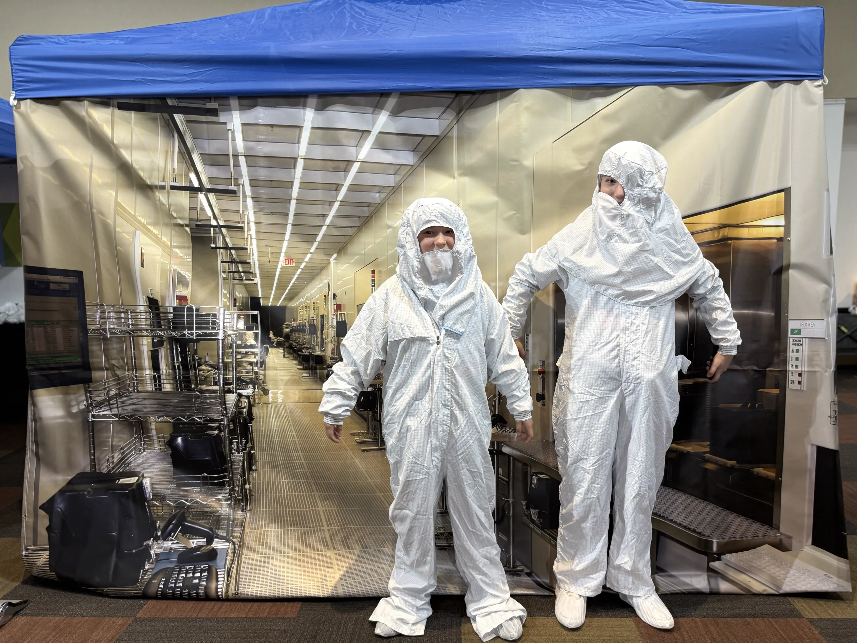
The future of technology depends on cultivating a strong and skilled talent pipeline. According to McKinsey Company, the global semiconductor industry could grow to $1 trillion by 2030, driven by surging demand across sectors like automotive, consumer electronics, AI, and clean energy technologies. That’s why the SEMIquest Pop-Up Exhibition at SEMICON West, October 8-9, 2025 in Phoenix, AZ, will bring the semiconductor story to life through immersive, hands-on learning experiences for students, educators, families, and the general public.What Is SEMIquest? SEMIquest is an engaging, interactive experience designed to introduce students in grades 7-12 to the world of semiconductors. The program features hands-on activities, direct interaction with industry professionals, and workshops for educators aimed at highlighting the essential role semiconductors play in everyday life and future career opportunities. Key Program Components:Students trying on NXP bunny suits at Semiconductor Adventure DayIndustry Engagement – Offering students the opportunity to interact with industry through the interactive exhibition space.Hands-On Activities – Highlighting careers in semiconductors and promoting STEM education for students.Educator Engagement – Offering teachers training and resources to carry lessons back into their classrooms.Field Trip to SEMICON West 2025 – Providing students an opportunity to attend SEMICON West 2025 at the Phoenix Convention Center in Arizona, with complimentary admission and curated tours that offer a behind-the-scenes look at the global semiconductor industry.Students from ASU Preparatory Poly Tech Campus Participating in Semiconductor Adventure Day and event led by the Semi Foundation and ASU PreparatoryThe program culminates in an on-site learning experience at the Arizona Science Center, located adjacent to SEMICON West 2025—where students can explore exhibits, engage with companies, and witness the semiconductor ecosystem firsthand.Projected Reach: In its inaugural year, SEMquest aims to engage 500-1000 students in grades 7-12, with a national expansion plan already in motion.Impact Goal: Reach 60,000 families and students during a 4-month Pop-Up exhibition in Arizona through targeted programming and outreach.Why This Work Matters: The Semiconductor Industry Needs TalentSemiconductors are the foundation of modern life—from smartphones to satellites, healthcare tech to AI applications, and more. Yet, many students are unaware of what semiconductors are or how to pursue a career in the field.The Semiconductor Industry Association (SIA) estimates the U.S. could see a shortfall of 67,000 skilled workers by 2030 in key roles that require postsecondary education.A 2023 Deloitte report warns of a global shortfall of 1 million skilled workers in the semiconductor industry by 2030 if proactive steps aren’t taken.Semiconductor Research Corporation 2023 findings indicate that while 577,000 students pursue four-year STEM degrees annually, only about 19,000 enter the semiconductor industry each year. This disparity underscores a significant gap between STEM education and semiconductor industry employment.SEMI's American Semiconductor Academy (ASA) Vision Paper highlights the importance of raising student awareness through educational and industry collaboration, offering hands-on experiences and real-world applications.Image Source: Photo courtesy of SRC (Semiconductor Research Corporation).The SEMIquest Pop-Up Exhibition tackle this urgent gap through meaningful engagement, accessibility, and experiential learning—helping students envision themselves as future leaders in the field.What Sets SEMIquest ApartReal Industry Involvement – Students interact directly with professionals, tools, and environments used in the field.National Scalability – While beginning in Arizona, the program is structured for national rollout.Cross-Sector Collaboration – A unique fusion of education and industry.Integrated Learning Model – Teachers and students learn together, amplifying classroom impact.Join the Movement: Shape the Future of InnovationWe’re calling on partners across the country to join this work. Whether you’re an industry leader, educator, or community-based organization, your involvement is essential to inspiring and preparing the next generation of innovators.Industry Partners – Showcase your work, engage directly with students, and contribute resources to the traveling Semiconductor Pop-Up Exhibition.Schools Educators – Bring your students, co-host hands-on workshops, and integrate real-world tech experiences into your curriculum.Foundations Funders – Support the expansion of this scalable model and help bring it to communities nationwide.Join us at SEMIQuest! To get involved or learn more, contact Perla DeBaggis at [email protected]. Perla DeBaggis is Sr. Specialist, Career Industry Awareness at the SEMI Foundation.
Read More
SEMI kicked off 2025 by hosting its annual Industry Strategy Symposium (ISS) gathering industry executives, government leaders, and research institutions to share insights on current and near-term business and market dynamics. Over the course of two and a half days, this key forum also provided valuable networking opportunities to foster collaboration.The event theme, Ready. Set. Ramp! aligns with the industry's goal of reaching $1T by 2030. While there is uncertainty due to global trade tensions, supply chain challenges, and talent shortages, AI-driven opportunities are proving to be a major growth driver. Another key highlight was the advanced packaging panel that reinforced the value of hybrid bonding and 3D device architectures playing a critical role in supporting AI and next-generation chips. The overarching sentiment from the event was that it's an exciting time to be in semiconductors, with unprecedented transformation and opportunities ahead. Collaboration across the industry is essential to overcoming technical challenges and accelerating innovation.SEMI leaders had the opportunity to speak with Francoise von Trapp of 3D InCites at the conclusion of ISS. Listen to the podcast to hear highlights from Joe Stockunas, President of SEMI Americas, along with market updates from SEMI’s Market Intelligence team members, with Inna Skvortsova covering semiconductor equipment and Christian Dieseldorff speaking on fab expansions. Looking aheadSEMI has many conferences and exhibitions scheduled throughout the year with opportunities for insights and networking. For the SEMI Americas region, don't miss the inaugural SEMIExpo Heartland on April 1-2 in Indianapolis, Indiana. SEMI is excited to host this event in the burgeoning Midwest U.S. region that is already seeing increased activity and opportunity for semiconductors, especially in areas around automotive electronics, smart manufacturing, machine learning, AI and workforce development. The expo is poised to spur collaboration among industry, government, and academia.A key change to note for Americas events this year is that SEMICON West is taking place in Phoenix, Arizona on Oct. 7-9. With over $100B in investments in motion, the greater Phoenix area is a growing manufacturing hub in the Southwest. There is already a lot of buzz and excitement with a sold-out venue and over 400 speakers lined up for the 3-day event. SEMICON West will return to San Francisco in October 2026 and will alternate between these two locations every other year through 2030.ResourcesPress Release: Eighteen New Semiconductor Fabs to Start Construction in 2025, SEMI ReportsPress Release: Global Total Semiconductor Equipment Sales Forecast to Reach a Record of $139 Billion in 2026, SEMI ReportsSEMI Market Intelligence ReportsSEMI ISS 2025: Ready, Set, Ramp! by Dean Freeman, 3D InCitesSEMI ContactSherrie Gutierrez, Marketing Communications ManagerEmail: [email protected]
Read More
Use of machine learning and artificial intelligence (ML/AI) is on an exponential rise across fields1 including all aspects of the semiconductor industry. In the last decade, the use of ML/AI exploded in the areas of speech recognition, facial recognition, smart phone features, search engines and now large language models like ChatGPT, Bard AI, and CoPilot. The ML/AI growth has been enabled by massive data storage capacity and increased compute performance, leading to projections for the semiconductor industry to reach over $1 trillion in annual revenue by 2030, with about 50% of the industry’s growth related to GenAI2. Figure 1: McKinsey Company on GenAI driving semiconductor industry growthAs semiconductor manufacturing drives toward Industry 4.0, SEMI member companies have a vision of Industry 5.0, truly adaptive manufacturing, integrating human creativity with robotic precision enabled by AI. Along that path, automation and data exchange in every step of manufacturing is essential, with data acquisition, data integrity and relevance, and operational Digital Twins3 as defined steppingstones to the factory of the future.Based on growing member interest in ML/AI, in 2019, SEMI assembled technology communities that quickly engaged in AI discussions and proofs of concept, discovering gaps in the path to Industry 4.0. Successful demonstrations of the value of AI in chip manufacturing process development and factory efficiency, not to mention GenAI uses in society, hastened the pace to produce faster, more powerful chips to accommodate the computation and communication requirements. Recognizing the industry opportunity and the mounting role AI plays in the semiconductor supply chain, SEMI initiated several thought leadership efforts, namely the Smart Manufacturing Initiative, Smart Data-AI Initiative, and the Future of Computing think tank.Smart Manufacturing According to the SEMI World Fab Forecast, over 100 new and expanded wafer fabs will begin volume production by 2027. This massive capacity expansion will need to achieve the highest possible operational efficiency and performance. To this end, the Smart Manufacturing Initiative is a technology community with over 120 member companies collaborating pre-competitively to transform manufacturing. The SEMI Smart Manufacturing Global Executive Committee (GEC), outlined a roadmap vision for the cognitive factory of the future based-on technology, sustainability and future talent. The GEC has been working with members to realize that vision. Figure 2 describes this vision in terms of the technology progression needed and the approximate timeline for implementation by most manufacturers. The proliferation of this vision through Smart Manufacturing Forums at SEMICON events around the globe, newsletters and blogs has garnered enormous interest and participation in the initiative and is central to the mission of connecting and raising awareness within the ecosystem. Figure 2: AI-Driven Smart Factory (Point Systems to Autonomous Solutions) To move the needle on this vision, industry experts in the initiative successfully created and launched the Industry 4.0 Readiness Assessment Model (IRAM) to help assess technology deployment progress. IRAM adoption is steadily growing. Modern front-end and back-end lines produce an extraordinary amount of multi-modal data from a variety of sources, and this is key to success in unlocking the potential of AI in manufacturing environments. The initiative’s global working groups on Data Architectures and Smart Control Room among others are working towards a holistic Cognitive Factory framework uniting the vertical and horizontal flow of information. Integral to the Cognitive Factory are smart manufacturing standards, that will accelerate the vision outlined above, and without which local solutions are unlikely to scale.In 2023, the Smart Manufacturing Initiative brought together industry leaders in a unique Digital Twin workshop to align on the state of semiconductor development and usage. The key takeaways from this workshop are captured in a white paper that highlighted the need to accelerate efforts in multiple areas including standards. Along with SEMI International Standards, Smart Manufacturing supports other standards development organizations (SDOs) and NIST standards development, for example, to identify and drive critical standards for Cognitive Factory implementation. The initiative is planning future workshops on Cognitive Factory Framework requirements, Digital Twins, and Smart Data AI in the coming months. that highlighted the need to accelerate efforts in multiple areas including standards. Along with SEMI International Standards, Smart Manufacturing supports other standards development organizations (SDOs) and NIST standards development, for example, to identify and drive critical standards for Cognitive Factory implementation. The initiative is planning future workshops on Cognitive Factory Framework requirements, Digital Twins, and Smart Data AI in the coming months.The GEC has identified critical interrelationships in addition to the technology focus. At the intersection with sustainability, the initiative has formed a collaborative task force with the SEMI Semiconductor Climate Consortium (SCC) to develop a bottom-up technology roadmap that can be used as a blueprint for device makers to meet their proclaimed sustainability goals faster. The task force organized a technical session at SEMICON West 2024 and will be releasing a white paper in the near future. Similarly, the initiative is working with the SEMI Foundation to identify necessary future skills and to make training available through SEMI University. Smart Data AI – Applying AI to Semiconductor OperationsSEMI’s Smart Data-AI Initiative started by assembling a group of interested companies to explore the pivotal role AI could play in the industry and to address the criticality of data. All stakeholders agreed that a formidable challenge was (and still is) the integrity of that data and the security of sharing that data, which is considered IP to most. The optimal implementation of ML/AI techniques can only be gained by access to the comprehensive data set which is owned by numerous supply chain partners. Consequently, semiconductor R D, process and design have not yet realized the full benefit of Data-AI advances. In response, the initiative developed a framework to create value for members and support industry progress. Four pillars underpinning the strategy are:Educating stakeholdersBuilding communitiesExecuting proof-of-concept projectsDeveloping industry standardsTo explore the data challenges the subject matter experts highlighted, a collaborative proof-of-concept (POC) project was proposed in 2019 and accepted by the initiative's partners at Army Research Laboratories4 along with academic and industry partners. The project has completed two phases and is starting on its third phase under the expert guidance of an Industry Advisory Council (IAC) comprised of leaders in the Smart Data-AI community.The POC project, being conducted by principal investigators at Cornell University, demonstrated significant accomplishments from the first two phases, including:An AI model to predict device geometry by optimizing photolithography and plasma etching processesInitial demonstration of secure data-sharing techniques with software-hardware co-optimizationInnovative metrology ideas to train AI algorithms rapidlyStudents trained in cross-disciplinary skills to address the industry’s critical talent shortageFurthermore, the visionary objectives laid out at the initial stages of the POC proved to be synergistic with the strategic goals of the CHIPS Act5, which articulates the need for “collecting, aggregating, and sharing data sets that enable benchmarking and operational improvements, tools development, the creation of digital twins, and training AI models,” and that “the NSTC could develop a methodology for the voluntary sharing of data that protects the proprietary component and national security while enabling access to appropriate performance data.” Phase 3, to be completed by August 2025, will advance the state-of-the-art toward the following specific objectives:A framework to create and integrate Digital Twins of semiconductor R D and manufacturing process toolsAbility to explore processes and generate virtual devices swiftlyDefined interfaces to combine models for each process module or toolAccurate AI-based models for executing virtual process flows to build virtual devicesAdvanced solutions for secure data-sharing across the ecosystem – for example, federated learning where raw data is protected for each entity by building models locally, and only the outputs of the local models are used to build flow-level AI modelsFoundation for future industry standards for secure data-sharing and for interfaces in the virtual innovation environmentSEMI continues to build the collaborative community for Data-AI and strives to synergize with broader efforts such as the Digital Twin Manufacturing Institute, NSTC, and NAPMP in the U.S., and international standards development. Smart Data AI – System-level Innovation for AI – Future of ComputingThe cross-collaborative and synergistic objectives of Smart Manufacturing, the Smart Data-AI proof-of-concept work, and SEMI Standards merge to advance the state-of-the-art. The objective is to help members realize the full value of technology and innovation. In addition to improving semiconductor operations using AI, the efforts also strive to enable SEMI members to participate in, and ultimately profit from, market growth opportunities. Continued progress in AI is crucial both for the industry’s march towards $1 trillion in annual revenue, and for continuing to realize AI’s benefits to society.There are some hurdles to overcome in such a dynamic market. AI models, and the data they process, are outpacing hardware advances, posing a major roadblock for continued progress. As GenAI becomes more pervasive, the performance and power challenges continue to multiply, and require significant innovation in both hardware and software. While individual companies will develop competitive products in this domain, the entire ecosystem needs to evolve in a synergistic manner. As a global industry association, SEMI can play an important role in ensuring this. SEMI started a series of workshops and technology sessions to develop the community and identify opportunities and challenges. The first in this series was a joint workshop with McKinsey Co., held in October 2023, with a focus on innovations in “Domain-Specific Architectures.” Strategically, it brought together thought leaders from three diverse communities - start-ups, investors, and SEMI member companies across the supply chain. This was followed by an overcapacity audience at the Future of Computing session at SEMICON West 2024, where we explored AI-specific hardware with leaders in academia and industry. The Initiative’s next planned event in October 2024 is a focused workshop that is designed to be highly interactive and bring together visionaries and thought leaders from across the value chain – materials, devices, architectures, algorithms, and critical enabling technologies such as photonics, chiplets, advanced packaging, and 3D and heterogeneous integration. The overarching goal is to identify pre-competitive collaborative actions that would help the entire industry. The “Future of Computing” is the broad path to the industry’s future success. While AI systems are the current major wave on this path, future waves may be about heterogeneous integration of photonics and other components, and ultimately, quantum technologies joining the mainstream. SEMI continues to monitor these future trends, strengthen the ecosystem and enable innovation through pre-competitive collaboration, and accelerate implementation through standards.SEMI is fostering today’s collaborations while helping the industry navigate the future of electronics.Melissa Grupen-Shemansky is CTO at SEMI, Pushkar Apte is a Strategic Technology Advisor and Leader of the SEMI Smart Data-AI Initiative, and Mark da Silva is Senior Director of the SEMI Smart Manufacturing Initiative.Definitions and References:1https://arxiv.org/abs/2405.15828 Eamon Duede, William Dolan, Andre Bauer, Ian Foster, Karim Lakhani2McKinsey Company3Digital Twins for semiconductor manufacturing operations are dynamic, predictive, data-driven virtual models of a physical asset, process, or an entire factory, constantly synchronized with its real-world counterpart through real-time data streams and analytics4Research was sponsored by the Army Research Laboratory and was accomplished under Cooperative Agreement Number W911NF-19-2-0345. The views and conclusions contained in this document are those of the authors and should not be interpreted as representing the official policies, either expressed or implied, of the Army Research Laboratory or the U.S. Government. The U.S. Government is authorized to reproduce and distribute reprints for Government purposes notwithstanding any copyright notation herein.5“A Vision and Strategy for The National Semiconductor Technology Center (NSTC)” published by the CHIPS R D Office.
Read More
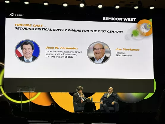
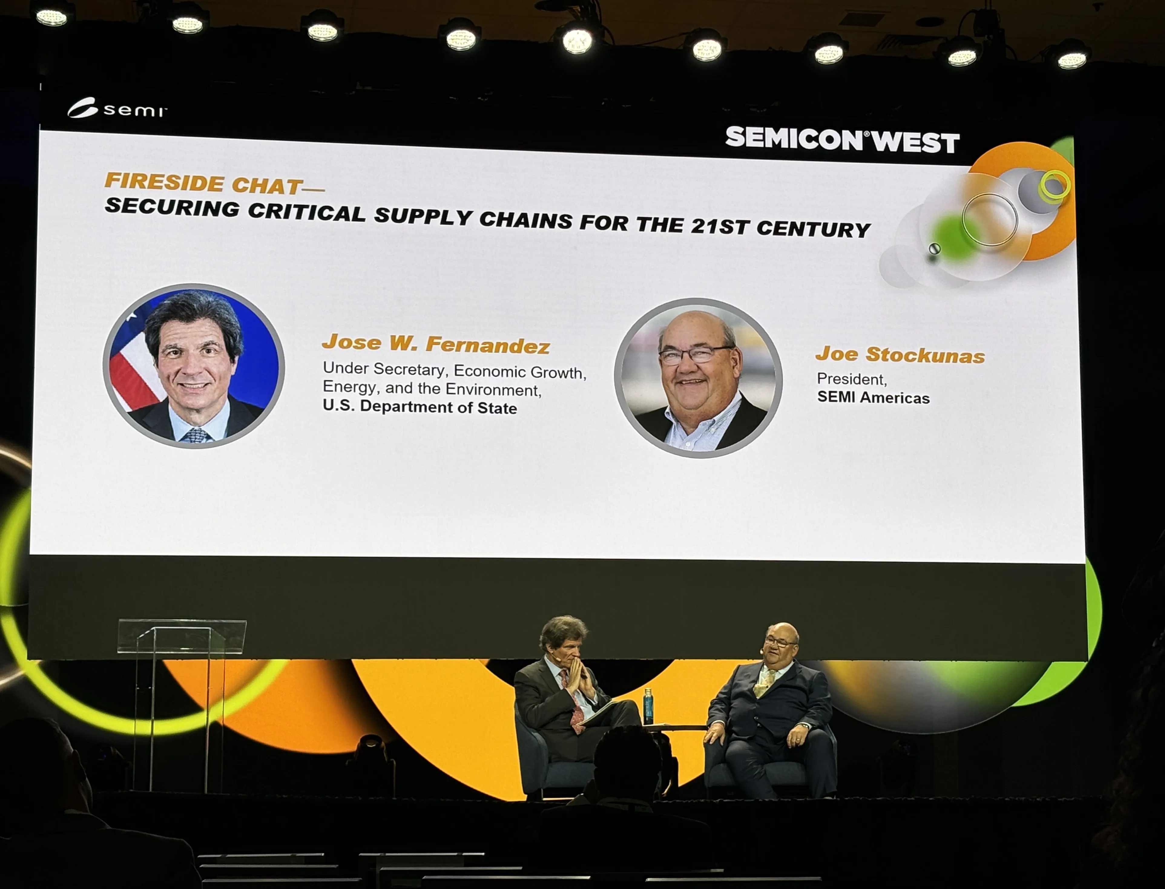
Jose Fernandez, U.S. Under Secretary of State for Economic Growth, Energy, and the Environment, sat down with Joe Stockunas, President of SEMI Americas, for a fireside chat on the CEO Summit keynote stage at SEMICON West 2024. In the Securing Critical Supply Chains for the 21st Century discussion, Fernandez emphasized the need to form partnerships to address vulnerabilities as the key to creating stable supply chains. It’s important to band together, he said, to protect our standards, values, and democracy. Diversifying the Global Mineral Supply ChainBecause chip fabricators depend on minerals like germanium, gallium, arsenic, indium, and rare earth elements, he highlighted how imperative it is for the industry to access them sustainably. To accomplish this, he stressed the importance of protection against supply chain bottlenecks in the mineral market. “According to a number of experts, we’re going to need 42x the amount of lithium by 2050, 25x the amount of manganese, and 25x the amount of cobalt,” he said. “Those minerals are basically controlled by one country, and that's a vulnerability.”To address these concerns, he shared that the State Department is working to strengthen the upstream and downstream portions of the semiconductor value chain, with the goal of supporting economic security across the globe. Foreign export controls, he said, have led to supply chain disruptions of key minerals, and bans on rare earth elements, processing equipment, and other technologies. As evidence of the State Department’s efforts to diversify, he highlighted the Minerals Security Partnership (MSP) and its work to seek mineral alternatives. Led by the U.S., it currently includes 13 other countries plus the European Union. Partnership and Investment Opportunities To further secure the industry's supply chain, Fernandez discussed the State Department’s efforts to partner with mining countries with untapped semiconductor resources. These countries, he said, also want alternate options for securing critical minerals. Fernandez highlighted Latin America as a key nearshoring focus area, pointing to the Americas Partnership for Economic Prosperity (APEP) as a solution for addressing obstacles to investment in the region. Obstacles, he said, include education levels, insecurity, and rule of law.To overcome such hurdles, he stressed the importance of fostering economic conditions that will attract investments, emphasizing the importance of workforce development initiatives and private sector involvement. “We don’t have enough trained workers in the U.S., and we certainly don’t have enough trained workers abroad,” he said. Fernandez shared that workforce development programs are being established through the U.S. Department of State International Technology Security and Innovation (ITSI) Fund, as well as private sector efforts and university partnerships. Currently, seven countries have been selected for ITSI funding, he said. “We’ve partnered with a number of universities to address the workforce gaps we see in our ITSI partners,” he said. “We’ve created workforce seminars, and we’re going to spend more time training the labor force.” These efforts supplement the work of the SEMI Foundation to develop a holistic workforce development program for the global semiconductor industry.Preventing Chips From Entering RussiaWith U.S. chips crossing into Russia through third parties, Stockunas asked Fernandez how the semiconductor industry could help address this. Despite existing sanctions against Russia, Fernandez shared that Russia still managed to import $1.7 billion worth of microchips from both the U.S. and Europe in 2023. To help slow this down, he highlighted additional due diligence for companies whose products often make their way into the country. The federal government, he said, speaks with these companies about complying beyond what the law requires.Fernandez shared that private sector cooperation with more stringent standards has been positive, noting that some companies have cut hundreds of distributors to further aid in prevention. In addition, he mentioned that sanctions have made a promising impact overall.“[Russia] has had to use outdated equipment, they’re engaging in counterfeiting, and they’re getting help from other countries,” he said. ​​Official SEMICON West Podcast In a podcast with Francoise von Trapp of 3D InCites recorded at SEMICON West, Fernandez discussed critical mineral partnerships, benefits and setbacks of regional supply chains, and chip sanctions against Russia. To learn more, check out the podcast interview with 3D InCites. SEMI Global AdvocacyDiscover how SEMI Global Advocacy Public Policy supports the microelectronics industry across trade, taxes, talent, and R D.John Cooney is Vice President of Global Advocacy and Public Policy at SEMI.
Read More
As more than 400 speakers took the stages at SEMICON West 2024, sustainability and workforce development stood out as two major focus areas. The second day of this year’s CEO Summit keynote program, themed Seizing the Global Opportunities and Challenges Ahead, featured sessions on both topics. One of the first sessions of the day was the Chief Sustainability Officer (CSO) panel discussion, titled Bracing for the Evolving Global Risk for the Semiconductor Ecosystem, moderated by Vice President of SEMI Global Sustainability Programs, Dr. Mousumi Bhat. Later that morning, Shari Liss, Vice President of SEMI Global Workforce Development Programs and Executive Director of the SEMI Foundation, moderated a fireside chat, Advocating for Real Change: Why Inclusion and Belonging Need to be Everyone’s Concern, with Sandra Mahadwar from KLA Corporation. Bhat and Liss were later interviewed for a podcast by Francoise von Trapp of 3D InCites to share additional insights on sustainability and workforce development, respectively. Bhat was also joined by Paul Kelly, COO of the New York Center for Research, Economic Advancement, Technology, Engineering, and Science (NY CREATES). Creating a More Sustainable Semiconductor Industry During their interview, both Bhat and Kelly emphasized that the industry will need to reduce its use of per and polyfluoroalkyl substances (PFAS) to sustainably innovate at today’s nanometer pace. For this reason, Kelly highlighted the importance of learning to balance current production demands with the health of climate.To achieve this balance, they discussed the efforts of the Semiconductor Climate Consortium (SCC). Much of the SCC’s efforts, they said, will focus on driving the industry toward net zero emissions. SEMI and NY CREATES announced a memorandum of understanding (MOU) at SEMICON West 2024 to promote sustainable practices within the industry, with a focus on PFAS reduction. Kelly pointed to the ability of SCC members to test new materials, gases, and chemicals at NY CREATES’ R D facilities in upstate New York to work toward replacing PFAS with more sustainable alternatives. Bhat also shared that this collaboration helps facilitate prototyping, experimentation, and tests and measurements for newer, more sustainable substances.Dr. Mousumi Bhat of SEMI and Dave Anderson of NY CREATES celebrate their organizations’ sustainability MOU at SEMICON West 2024.“The thought leadership comes from the Consortium, and the support on infrastructure comes from NY CREATES,” said Bhat. “This should become a blueprint to solve some of the challenging problems that we have in our industry.” When it comes to reducing emissions, Bhat mentioned two key objectives. The first, she said, is access to clean energy, and the second is the reduction of greenhouse gases. Bhat cited these as the issues that will take the longest for the industry to solve and pointed to the importance of industry collaboration and partnerships to support the needed experimentation. But while partnerships will bring the industry closer to net zero, both Bhat and Kelly cautioned that it won’t be reached overnight. “Much more needs to be done in the industry to reach that net zero goal,” said Kelly. “New chip technologies, new chemicals, and new processes are very much large leaps to achieving that. But right now, even some of the most advanced will only reduce [emissions] by 70%.” To help bridge this gap, Bhat encouraged others to join and participate in the SCC. “Rather than everybody doing a one-to-one experimentation in their own space and spending those resources, I would like to invite anyone that's not part of the climate consortium,” she said. “And [I invite] those that are part of the climate consortium to engage more actively, so that we are all accelerating the journey toward net zero.” Addressing the Talent Shortage This year’s SEMICON West also featured five keynote sessions dedicated to workforce development, as well as a Workforce Development Pavilion that included several talks around diversity, equity, inclusion, and belonging (DEIB). With the estimated one million jobs the industry will need to fill by 2030, Liss shared that every role is needed – from entry level all the way to Ph.D. researchers. “We need to try and bring in as many people as we can over the next few years,” said Liss. “The talent shortage is a global issue, not just a U.S. one.” Shari Liss of SEMI moderated the fireside chat at SEMICON West 2024 with Sandra Mahadwar from KLA Corporation.To begin to close the talent gap, Liss stressed the importance of educating children about the semiconductor industry. “We are just invisible to kids,” she said. “In every part of the globe, they carry chips in their hands all day every day, and they don’t know. So to me, breaking that barrier and making sure kids know about our work as an industry is going to be so critical to making this successful.” Liss also highlighted differences in workforce development programs across the world, noting that what works in one region may not translate to another. For example, apprenticeships are widely embraced in Europe, she said, but they’re a fairly new practice in the U.S. Conversely, she shared that veteran-focused programs wouldn’t work for some regions, but they’re a “powerful win” in the U.S. Each SEMICON show across the world, she shared, includes similar workforce development and DEIB programming, in addition to targeted sessions for students and HR professionals. Companies can interview for open positions at SEMICON shows as well. To learn more about SEMI’s workforce development initiatives and programming, visit semi foundation.org, or check out this overview of DEIB content at SEMICON West 2024. Samer Bahou is director of Marketing Communications at SEMI.
Read More
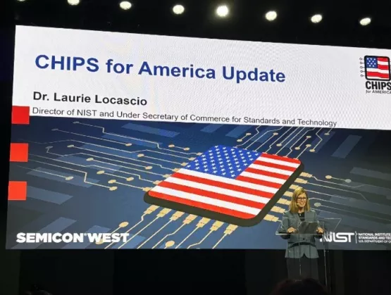
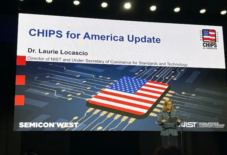
SEMI was honored to welcome U.S. Under Secretary of Commerce for Standards and Technology, Dr. Laurie E. Locascio, to the CEO Summit keynote stage at SEMICON West 2024 on Tuesday, July 9. Locascio, who also serves as the Director of the National Institute of Standards and Technology (NIST), delivered her morning CHIPS Act Update keynote address to a packed room of over 1,000 attendees at the Moscone Center in San Francisco.During her address, Locascio emphasized how far the U.S. chip industry has progressed since 2021. “Prior to 2022 and the passage of the CHIPS and Science Act, the U.S. produced 0% of the world's leading edge chips,” she said. “But now, after these proposed investments, we've changed the global landscape.”Industry Shifts from the CHIPS and Science ActDue to long delays and price increases resulting from supply chain vulnerabilities, Locascio shared that Congress began developing the CHIPS and Science Act with two key goals in mind. The first, she said, was to protect economic security, and the second, was to lower costs for American taxpayers. As part of the CHIPS and Science Act, CHIPS for America was established to advance semiconductor manufacturing in the U.S. CHIPS for America encompasses two offices: The CHIPS Research and Development Office, as well as the CHIPS Program Office - both of which are responsible for implementing CHIPS and Science Act law.CHIPS for America, said Locascio, couldn’t be another procurement program. Instead, it needed to be a purpose-driven approach to build domestic manufacturing capacity. Locascio highlighted that CHIPS for America galvanized several experts from the federal government, R D, and other core areas to work together to revitalize the U.S. semiconductor industry and increase capacity. To achieve this, Locascio pointed to CHIPS for America’s $30 billion in proposed direct funding and $25 billion in proposed direct loans.Locascio also noted diversity of technology as being essential for the American chip industry, citing how Intel, Micron, TSMC, and Samsung have recently expanded in the U.S., with SK Hynix planning to build a fab and R D facility in Indiana. No other economy in the world, she said, has more than two of these companies producing leading edge chips on its shores.“The total public and private investment from our four, leading-edge companies will equal roughly $300 billion between now and the end of the decade, far and away the most investment in new production in the history of the U.S. semiconductor industry,” said Locascio. Industry Investments on the HorizonTo further aid these efforts, Locascio mentioned CHIPS for America’s notice of intent to invest $1.6 billion in an open competition to accelerate advanced packaging domestically and encourage innovation. Funding will be directed toward five key R D areas, including equipment tools, power delivery, connector technology, chiplets, and Electronic Design Automation (EDA), she said. Additionally, Locascio shared that CHIPS for America recently announced its first preliminary memorandum of terms (PMT) to support the upstream supply chain, and shared plans to announce several more PMTs in the future. Lastly, Locascio revealed that CHIPS for America plans to release a model and process for bringing new facilities to life, in partnership with the National Semiconductor Technology Center (NSTC). NSTC members, she said, will gain access to partnership funds and state-of-the-art facilities to support the U.S. semiconductor industry. “Across all these efforts, from manufacturing incentives to research funding, to workforce development efforts, the U.S. must cultivate and build our competitive assets to protect and grow our technological leadership,” said Locascio.In a podcast with Francoise von Trapp of 3D InCites recorded at SEMICON West, Locascio discussed her career background, CHIPS Act investments and the path forward for the semiconductor industry in the U.S. To learn more, check out the podcast interview with 3D InCites. SEMI Global AdvocacyDiscover how SEMI Global Advocacy Public Policy supports the microelectronics industry across trade, taxes, talent, and R D.John Cooney is Vice President of Global Advocacy and Public Policy at SEMI.
Read More