downloadGroupGroupnoun_press release_995423_000000 copyGroupnoun_Feed_96767_000000Group 19noun_pictures_1817522_000000Member company iconResource item iconStore item iconGroup 19Group 19noun_Photo_2085192_000000 Copynoun_presentation_2096081_000000Group 19Group Copy 7noun_webinar_692730_000000Path
Skip to main content
Default Banner Image

SEMICON West

2025 was a fast-paced, exciting, and impactful year for the SEMI Standards team. We developed 14 new standards on crucial topics like supply chain traceability, defect mitigation, compound semiconductor materials, and so many more. In addition, we introduced the SEMI Global Standards Summit (GSS) in North America, where we created new standardization roadmaps and continued pertinent sustainability conversations from the inaugural GSS at SEMICON Japan 2024. We’re also excited to announce that we closed out 2025 with an impactful Q4. From December 17-19, we held our SEMI International Standards Meetings during SEMICON Japan. More than 15 Task Force meetings and 5 Technical Committee meetings were held, followed by an award ceremony. The brand-new Digital Twins in Manufacturing Task Force was also established to define and standardize a digital twin framework that supports consistent and scalable implementations. We published the new SEMI T27 standard in Q4, and we celebrated several outstanding volunteers for their contributions to the SEMI Standards Program at both SEMICON West and SEMICON Europa. As we reflect on Q4, it’s apparent how important collaboration is to the success of SEMI Standards. By working together, we lay the foundation for groundbreaking innovations in microelectronics manufacturing. The SEMI Standards team would like to extend a warm and sincere thank you to everyone who donated their time and expertise to define the future of our industry. These efforts would not be possible without your commitment and support.Still, it’s never too late to join the SEMI Standards Program. Learn more about membership and how you can help influence the next phase of semiconductor manufacturing. Q4 2025 HighlightsTakeaways from the International Standards Meeting at SEMICON JapanIn Q4, the SEMI Standards team held its International Standards Meeting at SEMICON Japan, where several task forces convened to set standards for compound semiconductor materials, information and control, traceability, and more. From December 17-19 at Tokyo Big Sight, the SEMI Standards team supported these technical committees in advancing several key standards revisions, including SEMI E181, Specification for Panel FOUP for Panel Level Packaging, and SEMI E182, Specification for Panel FOUP Loadport for Panel Level Packaging. In addition, a new Maintenance Robot Communication (MRC) Task Force was established with the objective of defining communication protocols and data exchange specifications between maintenance robots and equipment.The next SEMI International Standards Meeting will take place from May 11-14 in Albany, New York, during the SEMI Advanced Semiconductor Manufacturing Conference (ASMC). Digital Twins in Manufacturing Task Force Although the terms “digital twins” and “digital twin frameworks” are becoming more prevalent in the semiconductor industry, there’s still much debate on what they cover. To develop concrete, standardized definitions for each, the SEMI Standards team established the Digital Twins in Manufacturing Task Force in Q4. After the task force defines these crucial terms, it will then create definitions for internal digital twin components outlining baseline capabilities, discovery mechanisms, prediction quality metrics, unified model interfaces, and lifecycle management. Eventually, the task force will outline a framework for Digital Twins compatible with existing guidelines like SEMI Standard E133 or ISO 23247. The SEMI Digital Twins in Manufacturing Task Force is open to industry stakeholders. To participate, join the SEMI International Standards Program or learn more. Standards Awards at SEMICON West and SEMICON Europa SEMICON West honoreesQ4 was also a time to celebrate some of the talented individuals who make a difference in the SEMI Standards Program. At SEMICON West and SEMICON Europa, we honored 25 accomplished industry leaders across the following five award categories for their commitment and participation. Merit Award winners led projects to successful completion at the task force level. SEMICON Europa honorees: Judith Wittmann, Cristina Sanna, Peter Wagner, Friedrich Passek, Frank Riedel SEMICON West honorees: Dave Dunne of Applied Materials, Kirsten Smith of UCT/ChemTrace, Tommaso Orzali of ASML, Dr. Tyler Harrison of Teledyne MEMS, and Dr. Mary Ann Maher of SoftMEMSSEMICON Europa honorees: Christian Kranert of Fraunhofer IISB, Enrica Cela of Soitec, Hans-Christian Alt of the Munich University of Applied Sciences, and Ulrich Kretzer of Freiberger Compound Materials GmbHLeadership Award winners bolstered the SEMI Standards program through member recruitment, mentoring, and training efforts. SEMICON West honorees: Michael Potts of Arcadis, David Kandiyeli of KINETICS Equipment Solutions Group, and Per Nelson of Daikin AmericaSEMICON Europa honorees: Frank Riedel and Judith Wittmann of Siltronic, Cristina Sanna of GlobalWafers, and Jochen Ruth of Pall CorporationHonor Award winners have demonstrated long-term dedication to advancing SEMI Standards.SEMICON West honorees: Steve Martell of Nordson Test Inspection Americas, Lucian Girlea of Nikon Precision, and Dave Huntley of PDF SolutionsSEMICON Europa honorees: Peter Wagner of SEMI Standards, Fritz Passek of Siltronic, Arnd Weber of SiCrystal GmbH, and Frank Petzold of trustsec IT solutions GmbHCorporate Device Member Award winners are participants from the user community who act as corporate representatives for the SEMI Standards Program from the device manufacturer side. Stefan Radloff of Intel was honored with this award at SEMICON West. Technical Editor Appreciation Award winners are adept at translating complex technical information into clear and precise language. Dr. Alissa M. Fitzgerald of A.M. Fitzgerald Associates became the award recipient in 2025. Workshops at SEMICON WestOn October 8, the SEMI Voltage Sag Immunity Task Force hosted its Enhancing Voltage Sag Immunity workshop to address fab downtime caused by voltage sags. The workshop convened more than 20 industry professionals to review the limitations of SEMI Standard F47. They found that while 20% of downtime instances can be attributed to three-phase events, SEMI Standard F47 does not require testing for such occurrences. As a result, the Voltage Sag Immunity Task Force is developing a draft revision of SEMI Standard F47, scheduled for balloting in March 2026. If you missed this workshop, you can access the recording and presentation here. October 8 also saw the exciting return of the Analytical Workshop, hosted by the SEMI Liquid Chemicals Committee after a multi-year hiatus. This year’s workshop addressed near-term challenges and advancements identified by the International Roadmap for Devices and Systems (IRDS). It covered chemical quality and consistency, trace metallic impurities and improvements in ICPMS instrumentation, automated instrumentation for online measurements, detection for particle precursors and sub-10nm particles in liquids and on-wafer, and organic particle precursors identification using FTIR-ATR, SERS and AFM-IR. If you missed this workshop, you can access the recording and presentation here. The 2026 call for abstracts will be announced soon. Lastly, the SEMI Standards and SEMI University teams worked together to host Semiconductor Device Manufacturing in a Cleanroom, a workshop meant to introduce best practices for overcoming contamination problems in the cleanroom. By reviewing different sources of contamination, reviewing analytical techniques for quality control, and performing cleanliness testing, the course aims to help cleanroom facilities improve production reliability and yield.New and Revised Standards Released in Q4October 2025November 2025December 2025Get InvolvedSEMI Standards development activities take place throughout the year in all major manufacturing regions. To participate, join the SEMI International Standards Program.SEMI Standards are available through individual download purchases or online via SEMIViews. Watch this video to learn more about how SEMIViews offers a cost-effective and streamlined way to access 1,110+ SEMI Standards. Sign up for a 30-day SEMIViews trial.For more information, please visit the Standards website and events page. For any questions regarding SEMI Standards activities, please contact your local SEMI Standards staff.Paul Trio is Director of Standards at SEMI.
Read More
This year’s SEMICON West brought together industry experts from around the world to share insights on three of today’s most pressing topics: geopolitics, sustainability, and the semiconductor supply chain. From October 7-8, leaders from each field offered updates during SEMICON West’s Executive Panel Series, with each topic explored in its own hour-long session.Strategic Silicon: Geopolitics Shaping the Future of Semiconductors SEMICON West’s Executive Panel Series began on Tuesday, October 7, with a discussion on today’s geopolitical ecosystem and its impact on the semiconductor industry. Speakers compared the U.S. semiconductor landscape with China’s, highlighted supply chain strategies to mitigate disruption, and defined what it means to “win” the AI race. Mackenzie Hawkins from Bloomberg News moderated the panel, which featured Vince Jesaitis from Arm, Frank Heemskerk from ASML, Olivier Blachier from Entegris, Sarah Kemp from Intel, and Rich Ashooh from Lam Research.First, the panelists mentioned the U.S. CHIPS Act and the legislation’s attempt to diversify the semiconductor supply chain. Jesaitis added that countries are prioritizing supply chain resiliency, to which Kemp pointed to rising customer willingness to pay premiums for stronger supply chains. But what does it take to strengthen a supply chain? According to the panelists, a prevailing approach has been to regionalize operations. More regionalized supply chains can better withstand policy changes overall, but Ashooh noted that government regulations often can’t keep pace with innovation demands. China, in particular, may have key advantages in this respect. “The U.S. remains the most innovative environment in the world,” said Ashooh. “But if the Chinese government declared something a priority, the support will be there for it.” He also mentioned this arrangement allows China to advance in spurts.Kemp also stated that even with U.S. innovation and government incentives, the country faces longer construction times and greater policy complexity. Meanwhile, China is doubling down on its industry with resources and clear intent. Ashooh also added that China has more leverage in 2025 than it did during the first Trump administration. To address this, the panel recommended policy refinement to make U.S. trade relations more seamless. Furthermore, Heemskerk stated that the best government policies are often boring, advising governments to be predictable and reliable.The discussion concluded with mention of the AI race. Amidst discussion about what it means to “win,” Ashooh offered a simple explanation. Winning, he said, is seeing only customers in front of you instead of competitors. Sustainability Panel: Path to Success—The Semiconductor Industry Leads the WayAfter the Geopolitics panel, the stage swiftly transitioned to a new discussion centered on sustainability. Speakers included Elena Kocherovsky from Applied Materials, Beth Elroy from Micron, Joshua Kang from Qualcomm, and Sanchali Bhattacharjee from Google. SEMI’s Mousumi Bhat moderated this session.It may come as no surprise to learn that sustainability is reaching a critical juncture. According to the Climate Clock, the world has just under four years to address climate change before it becomes irreversible. Bhat pointed to this figure, emphasizing the mounting importance of industry-wide collaboration to make a tangible difference. With such a tight window for change, the panelists explained what’s being done to address these issues. Using AI to strengthen climate data, for example, came up several times. For instance, Sanchali mentioned that AI can bring in new data parameters to solve issues much faster. “We’re sitting at an inflection point where we have to harness the power of data,” she said.Elroy also shared opportunities to replace aging infrastructure with more sustainable equipment, as well as creating products that consume less energy from the start. However, distraction from climate goals is still a significant risk. Kocherovsky highlighted the industry’s limited resources, underscoring the importance of allocating them to efforts that move the needle. She cited clean energy adoption, noting that 80% of the industry’s emissions come from electricity. Fortunately, mitigation efforts are underway. Kang pointed to Qualcomm’s sponsorship of AI-powered air quality monitoring devices in Thailand, while Kocherovsky also touched on Applied Materials’ new sustainability projects. These efforts, while substantial, are nowhere near exhaustive. Tangible work is being done across the entire semiconductor ecosystem to make its solutions more sustainable, but it’s only the beginning. Charting the Course: Futureproofing Your Supply ChainsAs supply chain security has risen in priority, Wednesday’s panel detailed the industry’s efforts to strengthen it. Although COVID-19 exposed the urgent need for more resilient semiconductor supply chains, core issues have existed long before then. To explore this topic, I engaged speakers from across the value chain, including EMD’s Steven Johnston, AltaScient’s Rekha Menon-Varma, GlobalFoundries’ Roger Kao, Polar Semiconductor’s Surya Iyer, and Cisco’s Aman Aflaki. Today’s supply chain risks are enormous. From geopolitical tensions to natural disasters and cybersecurity threats, the semiconductor supply chain must withstand several intense and ongoing conditions. Because of this, the panel stressed the importance of early warning awareness and building buffers to counter setbacks. Creating buffers, Aflaki said, leads to necessary redundancies like using digital twins when feasible or engaging with second-and third-tier suppliers. Today’s customers, he said, also tend to be more focused on resilience and risk management rather than cost. Another emerging risk management solution is to use AI to build scenario models before incidents happen. As AI technology advances, companies that adopt it sooner rather than later could gain a competitive advantage. Johnston also added that AI could lead to more efficient R D and material sourcing. In addition, the panel pointed to the growing worldwide shift to regionalize supply chains. Menon-Varma highlighted that each country is approaching this in its own way, with many new global partnerships arising due to U.S. tariffs and export controls. Kao also reinforced today’s “local-for-local” supply chain trend.Finally, the panel ended with a discussion on collaboration. Although most leaders cite collaboration as crucial for the industry’s future, Johnston noted that working together is often halted by IP concerns. To address this, Iyer pointed to organizations like SEMI that unite key players to solve industry-wide problems.SEMI would like to thank all speakers, sponsors, and attendees for the success of this year’s Executive Panel Series. Bettina Weiss is Chief of Staff Corporate Strategy at SEMI.
Read More
The 2025 SEMICON West Market Symposium brought together leading analysts and strategists to decode the powerful forces shaping the global semiconductor market. Building on last year’s focus on fabless growth and workforce initiatives, this year’s sessions centered on the rising influence of geopolitics, trade policy, and AI-driven investment. Experts from SEMI, Integrated Insights, Boston Consulting Group, Kearney, PwC, WSTS and TechSearch shared perspectives on how global shifts from tariffs to technology races are redefining supply chain resilience and regional competitiveness.On October 6 in Phoenix, Arizona, Clark Tseng, Senior Director of SEMI Market Intelligence, hosted the symposium and presented along with industry experts on the current trade environment from various angles. Discussions ranged from the effects of U.S. tariffs across the globe, to sector-specific considerations and market growth areas. US Trade Dynamics in Semiconductors As the geopolitical landscape in the U.S. becomes more complex, Iacob Koch-Weser, Associate Director, Global Trade Investment at Boston Consulting Group outlined the impact that tariffs are having on the U.S. industry. The average American tariff, he said, is higher than any time in the last 75 years. Although the semiconductor industry is less affected by high tariffs than other sectors, Koch-Weser noted that might change with the administration’s expanded Section 232 Tariff that imposes 50% tariffs on steel, aluminum, and their derivatives on nearly all trading partners. To explain, he described four potential Section 232 tariff scenarios, underscoring limited Section 232 enforcement as the ideal approach.Tariffs may be deprioritized in favor of chips incentivesThere may be targeted carveouts for alliesThe administration may impose high tariffs with limited exceptionsThere may be a 100% tariff rate To cope with tariff uncertainty, Koch-Weser recommended that companies consider reshaping policies, mastering trade compliance, and reconfiguring supply chains if possible. He also shared four potential outcomes for the future of U.S. trade that could take effect within the next 18-24 months. The U.S. may run its own system while the rest of the world aligns to World Trade Organization (WTO) rules.North American countries may form a stronghold, leaving all other countries to choose between the North American alliance and WTO standards.Countries may form new blocs and preferential agreements, creating multiple economic spheres worldwide.Global cooperation could break down, forcing countries to fend for themselves.With everything considered, he reinforced that the U.S. is still an attractive place for semiconductor investment. The current administration, he said, recognizes the importance of bringing advanced technologies back to the U.S. Navigating Uncertainty: AI-Driven Growth and the U.S. Semiconductor Manufacturing RenaissanceContinuing discussions on tariffs, SEMI’s Clark Tseng painted a picture of the current U.S. semiconductor industry. He divided his presentation into four key areas: near-term economic uncertainty, AI changes everything, semiconductor market equipment forecast, and material market outlook.Near-term economic uncertainty: U.S. tariff policies are contributing to inflationary pressures and altering global trade patterns, leading to cross-border uncertainty that is slowing investment. U.S. tariff revenue, he said, has expanded from $7 billion in January 2025 to $29.5 billion by August, forcing companies to sacrifice margins to compensate. AI changes everything: By 2030, Tseng noted that nearly half of the semiconductor industry’s capital expenditure will be driven by AI, pointing to sustained growth in AI-driven cloud infrastructure spending through 2028 forecasts. AI is also moving beyond data centers into edge computing and endpoint devices.Semiconductor market equipment forecast: Tseng reported that the outlook for the equipment market remains strong over the next three years. However, the biggest risk to the market is a potential slowdown in AI investment and adoption. Additionally, U.S. export controls and changes in regional supply chains present some challenges. Last year, China was the largest market for semiconductor equipment, but Tseng expects continued normalization amid broader market adjustments. Taiwan and South Korea experienced the strongest year-over-year growth, driven by demand for AI chips and high-bandwidth memory (HBM). Material market outlook: Silicon wafer shipments grew strongly in Q2 of 2025, but Tseng flagged this as unexpected and cited tariffs as a possible explanation. He noted the 300mm wafer segment is expected to grow 7% in 2025, while 200mm is projected to decline. The total wafer material market, he said, is also expected to grow by 6% this year. Additionally, wet chemicals experienced a 16% expansion in 2025, while silicon wafers, photolithography materials, and CMP materials are in recovery. Semiconductor Market – Status Outlook Tobias Pröttel (or Proettel), CEO of World Semiconductor Trade Statistics (WSTS), reported that the industry’s rebound remains firmly on track, with the latest WSTS statistics confirming a 19% year-over-year increase in global semiconductor sales during the first half of 2025. Total revenue reached $346 billion over the period, supported by strong demand for AI-driven infrastructure and next-generation data centers. Based on this solid first-half performance, WSTS has raised its full-year 2025 forecast to $728 billion, representing 15% annual growth, and now expects the market to reach around $800 billion in 2026, keeping the industry on course toward the $1 trillion milestone before the decade’s end.Logic and Memory continue to lead the expansion, driven by GPUs, AI accelerators, and high-bandwidth memory (HBM), while other product categories are showing steady recovery after the recent downturn. Pröttel noted that this growth is not confined to a single region: the Americas, China, and Asia Pacific are all posting double-digit gains, reflecting strong global momentum across the semiconductor value chain.Strategic Approaches to Semiconductors by Major Economies Following Pröttel, Kearney’s Vice President, PERLab, Sanjay Kumar outlined the semiconductor investment climates in South Korea, Japan, Taiwan, and India. South Korea is currently focused on maintaining its lead in memory, diversifying into logic, localizing its supply chain, developing advanced packaging capabilities, and investing in startups. Kumar also noted the Korean approach of offering loans, as opposed to the U.S. strategy of providing direct grants. In addition, Kumar said the Korean government plays an active role in how it wants its companies to grow, whereas the U.S. takes a more passive approach in this regard.Japan is also honing its leadership in key areas like materials and memory, and Kumar also pointed to the country’s efforts to build additional advanced packaging capacity. Japan, he said, aims to grow its industry though a mix of grants, loans, and tax credits. Among the country’s notable subsidies include a 50% subsidy for TSMC – its largest so far – as well as a $4 billion subsidy for Rapidus. Taiwan’s semiconductor industry is critical for protecting its national security. As a region with limited land, power, and water, Kumar noted that Taiwan is currently focused on developing its talent base. Its government is offering tax credits for R D and equipment and up to a 50% cost share for R D projects. India, he said, has one of the most ambitious incentive programs in the world. Through its India Semiconductor Mission (ISM), the country offers a 50% federal subsidy, in addition to a 20-30% state subsidy in its quest to cover the entire semiconductor ecosystem. Kumar also spotlighted some of India’s successes – like the joint venture between Renesas, CG Power and Industrial Solutions, and Stars Microelectronics – to build a new OSAT facility.Adapting to New Policy and Navigating the U.S. Semiconductor Landscape – Insights from Taiwan Taiwan is a critical trade partner of the U.S., ranking fourth in total trade volume as of July 2025. With Taiwan’s stronghold on the U.S. chip ecosystem, Paul Poliakov, Senior Manager, International Tax Services, CPA at PwC Taiwan detailed both the bottlenecks and developments regarding Taiwan companies’ investments in the U.S. Among the investment bottlenecks he highlighted were higher costs of building facilities in the U.S., multiple layers of compliance requirements that may be intimidating for new market entrants, and complex visa and tax regulations. In addition, Section 232 investigations on semiconductors are ongoing, with several potential policy changes that could take effect. The pending United States-Taiwan Expedited Double-Tax Relief Act could help ease burdens, he said, but it has yet to pass in the U.S. Senate as of October 2025. If it passes, it will integrate benefits for Taiwanese individuals and businesses into the U.S. tax code, which could substantially benefit Taiwanese investment in the U.S., including manufacturing, services, distribution, and a wide variety of other industries. Furthermore, Poliakov suggested that businesses maintain flexibility in their investment strategies, engage with U.S. state and local governments that can offer investment incentives, and work with professionals to ensure regulatory compliance. Geopolitical Shifts in Advanced Packaging AssemblyIn the final presentation of the 2025 Market Symposium, Jan Vardaman, Founder and President of TechSearch International provided an overview of the current advanced packaging market. Although advanced packaging represents the highest growth area in the industry, Vardaman highlighted that packaging complexity is also soaring. R D, testing, and equipment support infrastructure, she said, are becoming more critical for meeting future packaging needs. Even though assembly is mostly done in Asia, new U.S.-based advanced packaging facilities from Amkor, TSMC, and others represent signs of change. Still, Vardaman noted that the U.S. has almost no capability to produce advanced IC substrates using build-up film, which are needed to support high density applications. In addition, she highlighted that building more silicon fabs on U.S. soil won’t solve its national security or supply chain concerns.For the U.S. to create a sustainable packaging ecosystem, Vardaman concluded that support of assembly facilities is crucial. Ultimately, businesses must be willing to pay more for U.S.-based packaging in favor of potential supply chain resilience and national security benefits. SEMI would like to thank all speakers, sponsors, and attendees for the success of this year’s Market Symposium. Explore the latest SEMI Market Intelligence reports, covering historical reporting, actionable foresight into emerging trends and technology investments to make confident, forward-looking decisions across the semiconductor and microelectronics value chain.Clark Tseng is Senior Director, Market Intelligence Team at SEMI. Nishita Rao is Director, Product Marketing at SEMI.
Read More
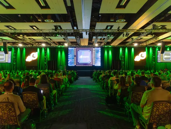
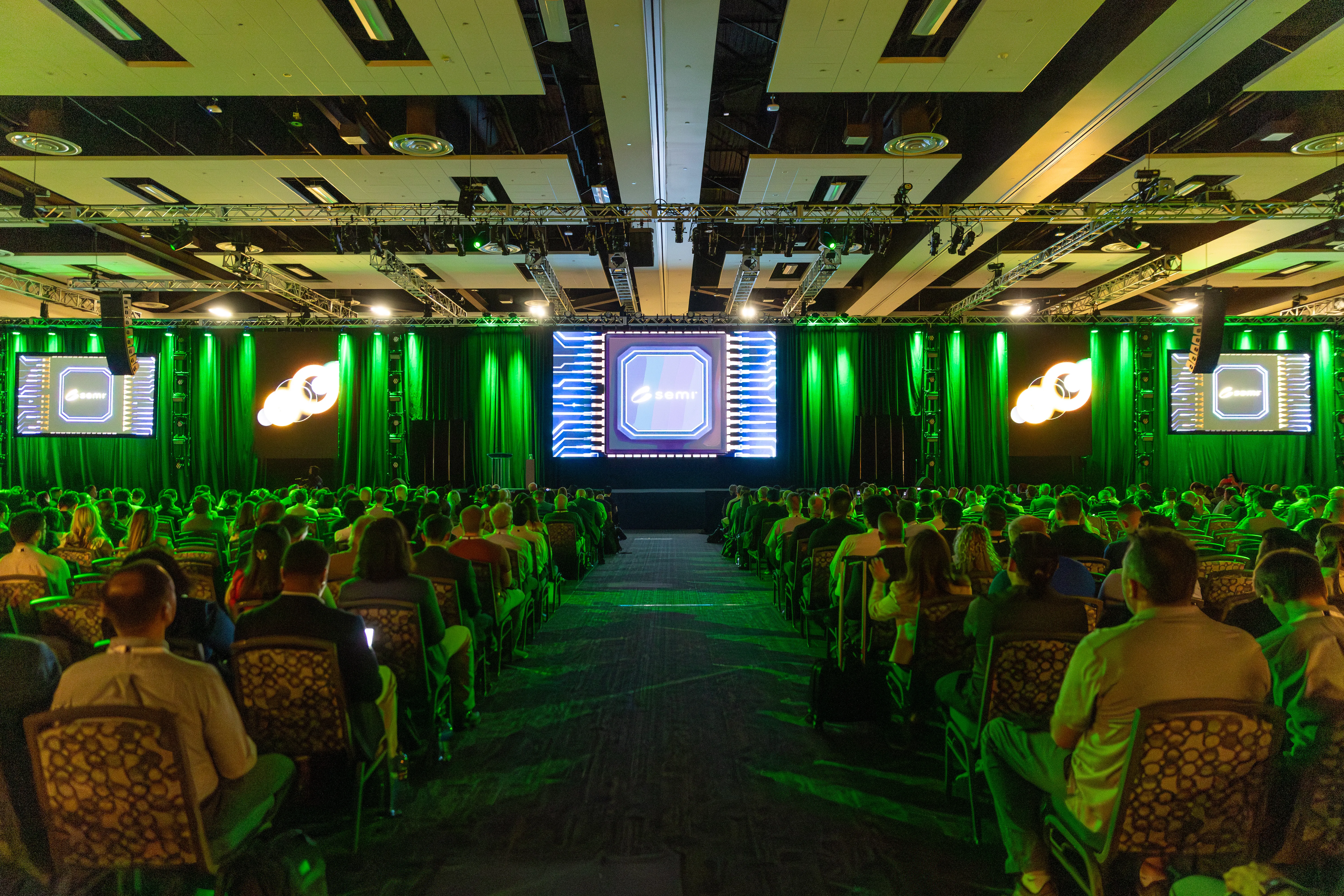
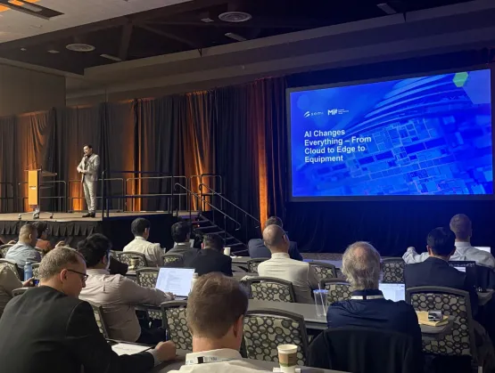
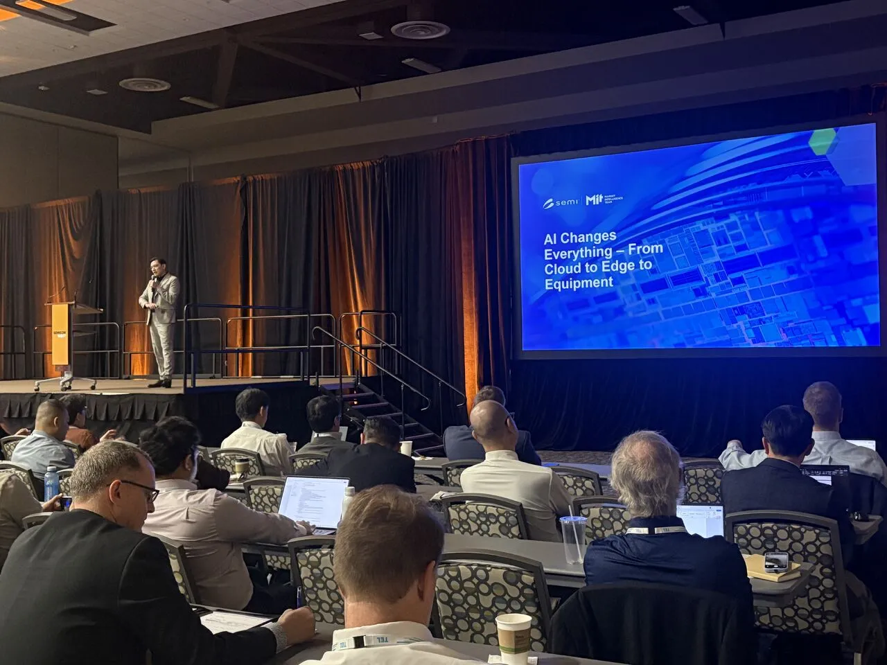
SEMICON West 2025 marked a year of many milestones. Not only was it the first SEMICON West ever to take place outside of San Francisco Bay Area, but it was also its largest exhibition in over 18 years. This year saw a 45% increase in booths, along with a 60% surge in registrations over 2024. The CEO Summit Keynote Series also returned to SEMICON West, featuring 14 unique presentations from October 7-9 at Arizona’s Phoenix Convention Center. Top leaders from both government and industry shared insights on a range of pertinent topics, from technology innovations, to emerging partnerships, sustainability and supply chain initiatives, and more. The keynote series began with opening remarks from SEMI’s President and CEO, Ajit Manocha, who urged audience members to focus on strategies that drive the industry forward and reinforced the importance of collaboration. He also outlined SEMI’s current priorities, including mitigating talent shortages, environmental disruptions, and geopolitical volatility.For those who missed the CEO Summit Keynote Series, this blog offers a summary of each presentation. The State of Arizona“In Arizona, vision becomes opportunity, and opportunity becomes action.” – Katie HobbsSEMICON West’s keynote series kicked off with Arizona Governor, Katie Hobbs, who underscored the expansive growth of Arizona’s semiconductor industry. She highlighted TSMC’s $165 billion investment in Arizona, the largest foreign direct investment in the state’s history, as well as more than 60 other semiconductor expansions that have taken place in the state. There are several reasons, Hobbs said, why Arizona has become an attractive place for semiconductor companies. The local talent base is one, with Arizona ranking among the top five states in the country in this area. Hobbs also highlighted Phoenix’s reliable energy grid, pro-business climate, and 100-year plan for water.AI in Every Layer: Future-Ready Strategies for Technology and Talent“This much disruptive innovation can’t be done by any one company. It requires a broad collaboration ecosystem.” – Sesha Varadarajan Following Hobbs, Sesha Varadarajan from Lam Research discussed AI-related challenges and budding solutions that address them. With AI setting the pace of industry innovation, Varadarajan emphasized the need for clarity for device-specific roadmaps. For example, logic is transitioning from FinFET to Gate-All-Around, DRAM is moving toward 3D architectures, and advanced packaging innovations are enabling continued scaling. Ultimately, Varadarajan concluded that device roadmaps would come down to three things: thinner materials, taller structures, and smaller features. Lastly, he noted that workforce development training often lags behind industry demand, highlighting Lam Research’s Semiverse education platform as a solution. Stronger Together - Building a Resilient Future for Semiconductors“When you’re working at an atomic level of precision, every detail matters.” – Jon KempDupont’s Jon Kemp offered insight into how the semiconductor industry can usher in a new wave of transformation. To achieve this, he highlighted three strategic priorities: supply chain, sustainability, and AI. Kemp emphasized bringing manufacturing closer to customers, designing products for energy efficiency, and creating new AI architectures that address mounting performance expectations. He also announced that Qnity, an integrated material solutions provider, will be spinning out of DuPont on November 1, 2025. Where Vision Meets Execution: Global Executive Summit (GES) Unites Industry Leaders“[There has been] lots of progress so far, and we want to build on that momentum.” – Carolin Seward. Carolin Seward from Google took the stage to discuss the upcoming Global Executive Summit (GES) from December 15-16 in Tokyo. This invitation-only meeting will convene industry executives to discuss core sustainability issues, like advancing abatement, pursuing gas substitution, driving green materials, and enabling low-carbon energy. Closer to Home: Costa Rica as a Partner for Successful Operations in the Western Hemisphere“Costa Rica is ready to become part of the solution.” – Manuel Tovar RiveraManuel Tovar Rivera discussed Costa Rica’s efforts to bolster its semiconductor industry. With its close proximity to the U.S., three decades of advanced manufacturing experience, and free trade, Rivera also explained the benefits of U.S. and Costa Rica collaborations. To meet the needs of its trade partners, Costa Rica is developing its local talent base, attracting foreign professionals, offering incentives for R D and startup investment, and streamlining its regulatory processes. Advancing 3DIC Technologies to Propel AI Innovations“Our best day is still ahead of us.” – Jun HeClosing out the Tuesday keynote series was TSMC’s Jun He, who spoke about the packaging innovations that are pushing the world closer to more advanced AI. The key benefit of advanced packaging, he said, is to enhance AI performance and efficiency–but excellent yield is a nonnegotiable requirement. He underscored the growing importance of CoWoS, or Chip-on-Wafer-on-Substrate packaging structures, as well as fluxless thermocompression bonding, to help meet demand for AI. AI Supercomputing for Next Generation Semiconductor Design and Manufacturing“AI factories transform electricity into intelligence.” – Timothy CostaNIVIDA’s Timothy Costa began the Wednesday keynote series by highlighting physical AI as “the next trillion-dollar industry,” and outlined how the company is helping the industry get closer to that benchmark. Costa noted the three NVIDIA computers being used to train physical AI models – Omniverse for simulation, DGX for training, and Jetson AGX for deployment. All of these, he said, need to work together to deliver on physical AI promises, like robotics, autonomous vehicles, and others. Executive Panel – Powering the Next Decade: AI’s Impact on Semiconductor Infrastructure and Market“We’re living in the most exciting time in the world of computing.” – Mukesh KhareFollowing Costa, the CEO Summit Keynote stage transitioned into a panel discussion with industry-leading AI experts – including Laura Matz from Merck KGaA, Darmstadt, Germany, Mukesh Khare from IBM Research, Mark Dougherty from TEL, and Angada Sachid from ASM. The panel was moderated by David Anderson, President of NY CREATES. Although there was much said during this 50-minute panel, a few key points were emphasized. First, Khare highlighted open chip design activities for AI models as a way to alleviate cost burdens. Design costs for more advanced nodes, he said, can be greater than $500 million. Matz also outlined the urgent need to develop PFAS-free materials without sacrificing yield. Currently, there are several areas where the industry doesn’t have a solution for PFAS, but AI models may be able to help.Sachid also mentioned power challenges, pointing to how one or two misplaced atoms can be the difference between a power-efficient versus a power-hungry chip. Deposition needs to be perfect at 10 trillion separate locations, and he pointed to AI as an emerging solution for this as well. However, despite the promises of AI, the panelists underscored that people are still a company’s most valuable asset. Revolutionizing Semiconductor Collaboration: The Emergence of AI-Driven Industry Platforms“You can make better decisions with more information.” – John KibarianWhile nearly every session touched on the need for industry-wide collaboration, John Kibarian from PDF Solutions focused on making this feasible. In today’s highly complex semiconductor supply chain, every point is critical, from fabless companies, to foundries, OSATs, and external vendors. To make industry-wide collaboration practical without compromising IP, he noted the importance of secure infrastructure, automated orchestration, and robust AI agents to assess and analyze the raw data that often goes unused. Kibarian highlighted PDF Solutions’ secureWISE system as a tool that’s already in place to address these needs. Shaping the Future of Semiconductors in the U.S.“The specific things that drove growth were the evolution of new applications.” – Giel RuttenAs the semiconductor industry continues its journey to $1 trillion in annual industry revenue, Amkor’s Giel Rutten provided an update on the U.S. market. Because OSATs are heavily concentrated in Asia, this poses a significant challenge for reshoring U.S. manufacturing. Most OEMs, he said, are looking to OSATs to handle several of their processes because it’s cheaper than doing it themselves. Rutten detailed the mounting complexities of backend assembly, including rising demand for multiple, high-bandwidth memory stacks that traditional SoCs can’t accommodate. This is pushing the industry toward heterogeneous integration, which further complicates the supply chain. Rutten concluded by emphasizing the importance of industry-wide collaboration, and noted that Amkor’s Arizona fab will offer a complete, turnkey supply chain in the U.S. Fireside Chat – Harnessing Digital Transformation to Empower People and Accelerate Precision“The more we double down on technology, the more we should also elevate humanity and double down on our values.” – Khadija Ben HammadaWith a strong emphasis on AI during the 2025 keynote series, the final discussion on Wednesday brought humans back into the spotlight. Khadija Ben Hammada from Merck KGaA, Darmstadt, Germany and Daniel Drellich from EMD Electronics (the electronics business of Merck KGaA, Darmstadt, Germany), joined Jon Krohn on stage for an insightful talk on empowering employees in today’s AI era. Of the many things discussed, both Hammada and Drellich underscored the need to build trust with employees, as many of them fear being left behind by the technology. While it’s true that companies have invested heavily in AI, such investments also require them to educate teams on how to use it. This can best be achieved through a culture, they said, where people feel comfortable enough to learn in the first place. The panelists also highlighted the importance of finding the right AI tools for specific purposes, instead of blindly choosing the most sophisticated solution. Partnering to Serve the Demands of the AI Era“A foundry business is a trust business.” – Kevin O’BuckleyAlthough there’s no shortage of discussion about the industry’s road to $1 trillion, Intel’s Kevin O’Buckley shared where that trillion-dollar value is being realized. Based on recent projections, the simple breakdown he presented shows that 50% is generated by fabless companies, 25% by suppliers, and 25% by foundries and OSATs. With the rise of fabless companies, he highlighted the need for foundries to provide value to customers, including better power delivery solutions and predictable execution on customer projects. He also shared Intel’s efforts, like bringing its 18A node into production, its PowerVia for backside power delivery, and new slurry formulations for delicate wafers. Bridging the Talent Gap: Accelerating Workforce Solutions for Semiconductors“We're building opportunity and innovation into the semiconductor workforce.” – Shari LissShari Liss, VP of Global Workforce Development and Initiatives at SEMI, detailed the current state of the industry’s workforce needs. More than 170,000 new workers, she said, will be needed in the U.S. in the next five years. To help close the talent gap, Liss shared a roadmap of the SEMI Foundation’s efforts, ranging from awareness programs that target children as young as seven, to apprenticeship programs for adults. So far, the SEMI Foundation has reached 1.25 million students through its apprenticeship and certification programs, 3,300 people through its expanded childcare access, and 7,000 people through its SEMI U courses. Liss also highlighted the SEMI Foundation’s operator role in the newly established National Network of Microelectronics Education (NNME) — a national program that aims to build regional centers around the U.S. for microelectronics education and training. Requests for proposals are now open, and applications are due in December. American Chip Revival and the Trusted Tech Imperative“Trust is the most important word in any language.” – Keith KrachThe 2025 keynotes series concluded with Purdue University’s Keith Krach and former undersecretary of state. During his time as undersecretary, he emphasized the importance of building trust to rebuild the U.S. semiconductor supply chain. Through his trust-first approach, Krach helped secure TSMC’s presence in Arizona, leading to better jobs and a stronger domestic chip ecosystem. In addition, he was instrumental in creating a clean 5G network that later became the xGTT, or the Global Trusted Tech Standard. SEMI would like to thank all speakers, sponsors, and attendees for the success of this year’s CEO Summit Keynote Series. Joe Stockunas is President, SEMI Americas.
Read More
Q3 2025 was packed with activity. From finalizing the Standards program for SEMICON West, to organizing the event’s corresponding Global Standards Summit (GSS), the Standards team is excited to share its most recent quarterly developments.On Tuesday, October 7, leaders from across the industry convened in Phoenix, Arizona, for the second annual GSS. This half-day summit focused on future standardization needs for supply chain traceability and environmental sustainability. In addition, the Standards team conducted two workshops at SEMICON West. The first, SEMI Liquid Chemicals Analytical Workshop, detailed recent advances in analytical methodology and instrumentation related to particle measurement, trace metals, and organics in liquid chemicals. The second, Enhancing Voltage Sag Immunity: SEMI F47 Standards Updates Insights Workshop, offered a forum for sharing improvements to SEMI Standard F47 to further enhance tool performance and reliability. Finally, Q3 saw the official introduction of SEMI Standards T26 and E195. SEMI T26-0925, Specification for Electronic Supply Chain Traceability Using Distributed Ledger Technology, will be crucial for improving security and transparency for the industry’s supply chain. Additionally, SEMI E195-0925 is now available for purchase. This standard, Test Method Using Adhesive Replacement Substrates to Assess Particulate Surface Contamination on Critical Chamber Components, offers a testing approach for measuring the ISO 14644-9 cleanliness of a critical chamber component.To participate in upcoming standard developments, learn more about becoming a member of the SEMI International Standards Program. Global Standards Summit The SEMI GSS made its North American debut at this year’s SEMICON West in Phoenix. Building on its inaugural event at SEMICON Japan 2024, GSS is a strategic forum dedicated to creating an industry-wide standardization roadmap for the next three and seven-year benchmarks. The 2025 GSS continued conversations from SEMICON Japan on environmental sustainability, while expanding its program to include supply chain traceability. As geopolitical tensions, mounting cybersecurity threats, and rising technological demands continue testing the limits of the industry’s supply chain, the need for global standardization is becoming increasingly apparent. The 2025 GSS program addressed these concerns and others across multiple sessions, offering insight on how these challenges are being addressed in the industry while highlighting critical areas still in need for standards development. Key outcomes from the GSS program include: Addressing data sharing across multiple supply chain tiers while protecting IP rights and a call for harmonization across standards. The presentation by Randy Hall from the Provenance Chain Network, offered approaches on how data owners can share information with authorized users without compromising sensitive manufacturing details. While there are standards gaps that hinder broader adoption, there is opportunity to address insufficient visibility across the industry’s supply chain amid ongoing cybersecurity threats by harmonizing across existing standards implementations. An integrated modeling framework for informing energy efficiency and carbon reduction approaches. Developed by the International Roadmap for Devices and Systems (IRDS) Environmental Sustainability for Semiconductor Facilities (ESSF) team, this effort helps address demands for maintaining rapid technological progress while still meeting the industry’s ambitious sustainability goals.Standardization opportunities for improving sustainability within manufacturing facilities. Nate Monosoff from Jacobs offered insight into the decision-making tradeoffs that balance sustainability with other facility performance areas, focusing on standard methods for calculating ESG performance. GSS concluded with a panel discussion that featured leaders from AMD, FTD Solutions, Intel, The Provenance Chain Network, Jacobs, Qualcomm, and Tokyo Electron. In this session, our thought leaders discussed the fundamental importance of standardization for our industry, standards adoption, incentivizing stakeholders, and how standards can be designed to remain flexible and adaptive as technologies and regulatory landscapes evolve. SEMI Standard T26In line with the 2025 GSS theme of supply chain traceability, the Standards team is pleased to introduce SEMI T26, Specification for Electronic Supply Chain Traceability Using Distributed Ledger Technology. This standard was published in September to define a secure and decentralized traceability system that all members of the electronics supply chain can safely share. This system is based on distributed ledger technology to improve industry-wide reliability assurance.Update on Document 7130CIn February, Document 7130C was approved during the North America Metrics Technical Committee Chapter Meeting. The document officially became SEMI E195 - Test Method Using Adhesive Replacement Substrates to Assess Particulate Surface Contamination of Critical Chamber Components in September.SEMI E195 describes a quantitative method for measuring the ISO 14644-9 surface cleanliness for particle concentration of a critical chamber component (CCC), by means of an adhesive replacement substrate. The purpose of this standard is to ensure measuring and reporting consistency across CCCs or processing equipment manufacturers. To help acquaint the industry with this standard, SEMI offered a combined, in-person course on SEMI E194 and SEMI E195 during SEMICON West. The course provided fundamental information on each standard, in addition to other process approaches for improving reliability and yield.Other SEMI Updates:SEMI Preventive Maintenance Automation White Paper SEMI Korea conducted a Global PM Automation Survey in August to better understand today’s preventive maintenance readiness issues for autonomous fabs. The results will be included in SEMI’s upcoming PM Automation Whitepaper and will ultimately guide future developments for related SEMI Standards. Standardized Semiconductor Cyber Assessment FrameworkIn Q3, the Semiconductor Manufacturing Cybersecurity Consortium (SMCC) released its Standardized Semiconductor Cyber Assessment (SSCA) framework. This document provides a detailed cybersecurity readiness plan for semiconductor companies across the supply chain. Its goals are to standardize industry-wide cybersecurity risk evaluations, establish and accelerate the adoption of best practices, and improve information sharing and collaboration. Download the SSCA framework for free.New Data Standard for Equipment Edge Governance In June, Document 6938C was approved during the Taiwan Information Control Technical Committee Chapter Meeting. The document officially became SEMI E196 - Guide for Equipment Edge Data Governance. SEMI E196 provides guidance for identifying equipment data supplied by manufacturers that can be used in equipment engineering or analysis applications.New Guide to Meet IRDS Yield Table RecommendationsAt the NA Summer Meetings, Document 6601B passed TC Chapter review with technical changes and a Ratification Ballot was issued in Cycle 7-2025. Pending final Procedural Review, Guide for Meeting IRDS Yield Table Recommendations for High Purity Polymer Materials and Components Used in Ultrapure Water, will cover areas that establish criteria for allowable contribution by critical components used for UPW treatment plant and distribution system. This document will be proactively updated to manage the risks associated with the high purity polymer materials used in the semiconductor process. The biggest challenges today are metals and particles and certain organics.Flex Standards Meeting at FLEX 2026Meet the leaders of the SEMI Standards Flexible Hybrid Electronics (FHE) Task Forces at Flex 2026, in Arizona, February 24-26, and learn about ongoing FHE standardization efforts!Standards Introduced in Q3 2025New and revised standards released in Q3. July 2025 StandardsAugust 2025 StandardsSeptember 2025 Standards Get InvolvedSEMI Standards development activities take place throughout the year in all major manufacturing regions. To participate, join the SEMI International Standards Program.SEMI Standards are available through individual download purchases or online via SEMIViews. Sign up for a 30-day SEMIViews trial.For more information, please visit the Standards website and events page. For any questions regarding SEMI Standards activities, please contact your local SEMI Standards staff. Paul Trio is Director of Standards at SEMI.
Read More
SEMICON West in Phoenix, Arizona, will bring together all of the SEMI Sustainability efforts and programs under one roof over three days. With back-to-back sessions from October 7-9, this year’s Sustainability EHS Program will offer expert insights on the most pressing sustainability topics facing the microelectronics industry. Tuesday will kick off the program and focus on the business aspects of driving to sustainability in the semiconductor sector. On Wednesday, the Pavilion hosts discussions on water risk, water management, circular economy solutions and the needs for innovation from startups. Finally, Thursday will highlight the current emissions landscape, milestones and achievements, and solutions developed by the SEMI Semiconductor Climate Consortium (SCC). The 2025 event also marks the first public discussions of the full scope, findings and status of the SCC’s direction.All three days of the Sustainability EHS Program are sponsored by Edwards, Schneider Electric, TEL, SCREEN, Sundt and the Greater Sacramento Economic Council. Here’s a sneak peek at what the 2025 program has to offer. Registration for SEMICON West is open.The Business of Sustainability – Tuesday, October 7 Sustainability Panel: Path to Success Sustainability hits the keynote stage with Tuesday afternoon with a panel discussion detailing a plan for meaningful sustainability progress. The panel, titled Sustainability Panel: Path to Success—The Semiconductor Industry Leads the Way for a Resilient Future, will take place on the CEO Summit Keynote Stage from 2:35-3:35 p.m. Experts from Applied Materials, BASF, Micron, Google, and Qualcomm will cover strategies on how collaboration, supplier engagement, and clean technology investments are reducing emissions and propelling the industry closer to its sustainability goals. Attendees will discover what’s working, what’s still to come, and how the industry will forge its way toward a more sustainable future.A Musical Performance by Ay YoungIn anticipation of the Path to Success panel discussion, Tuesday will also spotlight an exciting musical guest. AY Young is a singer, songwriter, and the founder of the longest-running clean energy concert series in the U.S. At 2:20 p.m., he’ll take to the CEO Summit Keynote Stage for a memorable performance and give a glimpse into how important sustainability has become to attract a new generation of talent. Through his musical talent and deep commitment to clean energy, Young was appointed as a United Nations (UN) Young World Leader in 2020, helping the organization further its 17 Sustainable Development Goals. His Project17 initiative is a 17-song album, with each song centering on a different goal and backed by a corporate sponsor that aligns with it. Young will also attend the Sustainability Reception from 5-6:30 p.m. at the Sustainability Pavilion Theater.EHS Regulatory OverviewThe wide range of regulatory topics will be showcased in the first session on Tuesday at the Sustainability Pavilion. Expert speakers and advocacy groups will deliver key insights on the threats and challenges, and the research and collaboration opportunities currently at play in the regulatory environment, with special focus on keeping electronics manufacturing strong. Climate Equity Social Impact Workgroup (CESI) Aligning with the theme of the UN Sustainable Development Goals, the SEMI Climate Equity Social Impact (CESI) Working Group will highlight how its members are progressing real-world outcomes for climate, education, and global cooperation. This session will run from 3-4 p.m. at the Sustainability Pavilion Stage, and it’s ideal for anyone in the industry who’s passionate about sustainable partnerships. Innovations Enabling Reduce, Reuse, Repurpose and Recover – Wednesday, October 8Resource Use and Circular EconomyWednesday’s 10:15-11:30 a.m. session, Resource Use and Circular Economy will offer tactical solutions to help fabs reach up to 80-90% circularity. The goal of this session is to lay a foundation for transforming the industry’s circularity concerns into practical opportunities, which will be achieved over two panel discussions. Discussion 1, A Circular Value Chain: Challenges and Leading-Edge Solutions, will highlight solutions for eliminating waste and reducing manufacturing costs through circular technologies. This panel will feature experts from Edwards, Syensqo, and ElectraMet and will be moderated by Subgeni’s Taimur Burki. These subject matter experts will highlight their company solutions, but also other areas they see in need of consideration from a circularity lens, as well as best known practices across fabs. Water is a precious resource, and how the industry manages it is crucial for its long-term success. Discussion 2, Tactical Maturity Scales for Water Management, will unveil two new guides developed by SEMI’s Water Management Working Group. Both products are designed to move manufacturers from both large and small fabs and manufacturing operations to assess their water needs and most efficiently improve water reuse by up to 80%. This panel will be led by speakers from Aquatech, SCREEN, Sundt, Ovivo, and C2MI. Water Resilience Starting at 11:30 a.m. at the Sustainability Pavilion Stage, attendees will hear from the SEMI Environmental Risk Mitigation and Reporting Working Group lead - Senior Sustainable Program Manager – Alua Suleimenova – as she shares her insights and findings from a recently completed study by WaterPlan on industry water risks within the semiconductor value chain. The topic and findings will then be addressed by a panel, where Suleimenova will engage leaders from ASM, Waterplan, ERM, and the Alliance for Water Stewardship, in a conversation about water, nature, and associated corporate risks. Although companies are making strides to protect water access, it’s becoming clear that a focus on internal activities will not move the needle significantly enough for achieving long-term resilience. This panel will offer solutions for adapting water-related risks to the supply chain, with a focus on North America, Asia Pacific, and Europe.Other Wednesday AttractionsSEMI S3 – Startups for Sustainable Semiconductors: SEMI S3, or Startups for Sustainable Semiconductors, is an annual program by the industry’s venture capital divisions designed to boost awareness of semiconductor industry needs by inviting promising startups to be mentored and pitch their solutions to our industry. Earlier this year, 145 candidates submitted applications. Now, it’s down to 15 finalists, who will present at SEMICON West from 2-4:40 p.m. at the Sustainability Pavilion, following a Fireside Chat from experienced innovation experts from 1-2pm.Accelerating Sustainability with Smart Manufacturing – Presentations Poster Session: Technical papers and posters focused on sustainability solutions – from water to energy – will also be presented in the Smart Manufacturing Pavilion from 2-5:15 p.m., providing an opportunity to network with industry leaders and discover the latest best practices for how machine learning and AI can reduce water and waste in fabs.Reducing Emissions – Thursday, October 9SCC – Tackling Emissions Across the IndustryExpect a full-house at Thursday’s all-day session featuring SCC – Tackling Emissions Across the Industry. From 10:15 a.m. to 3:00 p.m., the SEMI SCC leaders and experts will detail its findings and projects addressing the industry’s emissions. SCC has been focusing on ensuring consistent and measurable progress in decarbonizing from 2021 levels. Key topics include: Reporting and aligningBaseline, ambition, and roadmapAbatementLow Global Warming Potential (GWP) gases workLow Carbon Economy (LCE) access and procurementEnergy efficienciesScope 3 upstreamSEMICON West also features SEMI U courses to learn more about sustainability in our industry. For example, on Thursday, SEMI U: PFAS Compounds in Semiconductor Environment, is being offered from 8 a.m. to noon. This course is available for purchase. Support the SEMI Forest community effort to reforest our planet by funding a range of certified carbon avoidance and tree planting projects. Our goal for SEMICON West is to fund planting for 100,000 trees. Scan the QR code below to contribute and help us meet our goal.Learn more about the 2025 SEMICON West Sustainability EHS Program. Follow SEMI Sustainability on LinkedIn for regular updates on sustainability initiatives. Saifi Usmani is Vice President for Sustainability at SEMI.
Read More
AI is proliferating rapidly, fueled by ever-larger models and data sets that are expanding AI use cases and improving its accuracy. Future computing systems are now required to simultaneously deliver high performance, process large amounts of data, and use the least possible energy. The growing energy footprint of AI and the strain it places on the power grid is an increasing concern for companies and even entire countries. This could adversely impact future growth and could slow the semiconductor industry’s march towards $1 trillion in revenue, which is largely driven by AI applications.This is a formidable challenge that cannot be addressed in silos by individual companies or even industry segments. The SEMI Smart Data-AI Initiative is exploring how to overcome this challenge with collaborative and innovative system-level solutions that connect the dots across the entire AI system stack. In March 2025, we hosted a successful workshop, bringing together industry leaders across the value chain for a day of thoughtful discussions and knowledge sharing. Building on this foundation, we developed an exciting Smart Data-AI session to be held at SEMICON West in Phoenix, Arizona on October 7 from 10:30 a.m.-4:40 p.m. The “Future of Computing: Energy-Efficient Computing for AI and Beyond” forum will bring together executives and thought leaders across the entire ecosystem – including design, fabrication, interconnects, system integration, hyperscale architectures, advanced materials, and emerging technologies such as photonics and quantum. Attendees will have a unique opportunity to get strategic perspectives from these distinguished experts and learn about exciting future trends.Why Attend?Gain insights from global leaders and learn about innovative paths towards an energy-efficient computing future.Network and build cross-industry collaborations for the next wave of AI, photonics and quantum.Promote a more sustainable path for continued growth of AI to benefit humanity and the planet.Join the SEMI Smart Data-AI initiative to develop solutions and take concrete actions to reduce AI’s growing energy footprint.Support the industry in achieving its goal of reaching $1 trillion in revenue. Speaker Highlights Include:AMD • Ciena • Hewlett Packard Enterprise • IBM • Merck KGaA, Darmstadt, Germany •Microsoft • Quantum Economic Development Consortium • Rapidus • Rigetti •Siemens AG • Stanford UniversityDr. Pushkar P. Apte is the Strategic Technology Advisor and leads the Smart Data-AI Initiative at SEMI.
Read More
Digital Twins are no longer a futuristic concept in semiconductor manufacturing—they’re fast becoming the backbone of next-generation fabs. But here’s the challenge: without a robust, scalable data platform to unify, secure, and interpret the torrent of information flowing across design, manufacturing, packaging, and test, digital twins cannot deliver their transformative potential. At SEMICON West in Phoenix, Arizona on October 6, 2025 from 1–5 p.m., join us for a high-impact technical workshop that explores how advanced data platforms are fueling the next wave of innovation—enabling smarter, faster, and more precise decisions across the semiconductor lifecycle.What You’ll Learn – Gain insights on proven reference architectures for scalable data platforms, integration patterns that support digital twin ecosystems, real-world use cases from fabs and OSATs applying AI/ML at scale, best practices in managing governance and security across complex data pipelines.Modern Data Platform Architectures – Designed for speed, scale, and semiconductor precisionBreaking Down Silos – Leveraging shared ontologies and data fabrics for seamless interoperabilityAI-Enhanced Digital Twins – Real-world deployments across fabs and OSATsFederated Learning in Action – Secure, multi-party collaboration without compromising IPData Security Governance – Proven practices for high-stakes manufacturing environments Distinguished Speakers – Hear directly from leaders advancing digital twin and federated learning initiatives at the SmartUSA Institute and across the semiconductor ecosystem. Anshu Bahadur, Senior Program Manager, Technology Communities at SEMI, will open the workshop and introduce speakers who will share how they’re building these next-generation platforms and deploying them across fabs, OSATs, and the full manufacturing flow. Following individual presentations, the session will close with a panel discussion featuring these executives. Ross Kunz, Director of Technology, SmartUSA Institute (Keynote Speaker)Dr. Adam Schafer, CEO, Athinia TechnologiesDhara Vaishnaw, Head of Solution Architecture, AWSDr. Gautham Unni, Head of Solutions and Business Development, Semiconductor, AWSJonathan Holt, Senior Director, Product Management, PDF SolutionsDr. Surya Kalidindi, CEO, Multiscale TechnologiesWho Should Attend? This workshop is designed for: Data Platform Architects building the next-gen semiconductor backboneSmart Manufacturing Engineers integrating fab and test dataAI/ML Practitioners scaling models into production workflowsInnovators shaping digital twin systems for complex, high-precision manufacturing Why Attend? Because the future isn’t waiting. Digital Twins, powered by scalable data platforms, are redefining how the semiconductor industry innovates, collaborates, and competes. Don’t just keep up with the future—build it. Anshu Bahadur is Senior Program Manager, Technology Communities at SEMI
Read More
John Kibarian, CEO and co-founder of PDF Solutions and a member of the ESD Alliance (ESDA) Governing Council, will deliver a keynote during the CEO Summit at SEMICON West in October titled, “Revolutionizing Semiconductor Collaboration: The Emergence of AI-Driven Industry Platforms.” He recently shared with me a summary of what his talk will cover and his perspective on why collaboration is the key to growing the semiconductor industry to $1 trillion and how we will get there.Smith: What is the major industry evolution or dynamic that's making collaboration essential today?Kibarian: The semiconductor industry has dramatically evolved from a simple, linear process to a complex, collaborative ecosystem. Previously, everything happened at the wafer fab. Testing occurred at wafer sort, package yields were high, final testing was straightforward, and products were shipped. Collaboration was mainly between foundries and fabless customers, intensive during early qualification and test chip stages, then evolved to routine yield monitoring once production stabilized.Today's advanced packaging puts multiple chiplets into single packages, creating an explosion of test insertion points. This has driven up both test complexity and costs significantly. Front-end fabs now house the most complex machines, while test and assembly facilities, once relatively simple, now feature sophisticated system-level testers with integrated robotics. Assembly tools have become highly complex, with die-attach processes requiring increasingly tight tolerances. Success now requires collaboration across the entire chain, from system companies to equipment vendors, both for new product launches and ongoing production maintenance.Companies are adopting AI and machine learning (ML) to manage these complex production flows, whether for testing or equipment control. This demands even broader collaboration since AI requires combining data from multiple sources across foundries, fabless companies, OSATs, equipment vendors, and more, data that no single entity controls. What was once a straightforward handoff between two parties has become an intricate web of interdependent relationships requiring continuous coordination.Smith: Chiplets and chiplet-based architecture is in the news and seems to be a key solution or practical solution in response to the slowing down of Moore's Law. This demands incredible levels of collaboration and coordination across the whole value chain. Is this doable at scale where it starts to move into the mainstream?Kibarian: The semiconductor industry will need unprecedented collaboration to make chiplet manufacturing work at scale. But this can be done! Consider EUV lithography: Initially expected during the 65nm generation, it took years longer than anticipated despite being an incredibly complex technology. Extraordinary engineering was needed but it also required extensive collaboration between ASML, suppliers, customers, and the broader fabless community.If the industry achieved this level of coordination for EUV, it can do the same for chiplets. However, chiplet manufacturing will require even greater collaboration as more companies will build systems using chiplets from multiple suppliers.Today's chiplet-based systems typically source all components from one manufacturer, making standards like UCIe less critical since companies control their entire supply chain. This will change as companies increasingly use third-party components for cost-effectiveness.More and more, we will see systems using components from multiple players to get to market more cost-effectively. Consequently, future production flows will be significantly more complex, requiring coordination of substrates and base dies, third-party dies and interposers, OSAT and specialized testers with specific configurations.This orchestration must work not just for initial bring-up but for the ongoing production as well, and when reconfiguring chiplet combinations for different products, all requiring rapid, automated responses.All of that must be automated for quick reaction. Considering the complexity of the manufacturing flow, people will want to apply AI/ML to anticipate what is going on in each individual product built.Manual oversight of every chip and package during manufacturing isn't feasible at scale. Automated AI agents must handle this monitoring and quality control. Expanding this automation will require close collaboration between the manufacturing entity and engineering teams at the product companies.This will also require a different level of alignment and orchestration across all the software packages managing this complex multi-company process. The financial enterprise resource planning (ERP) systems know where material is going, what the demand is, and what the forecasts are. While separately, the manufacturing execution systems needs to know which tools are going to be available when. Most often, these manufacturing systems operate in factories the product company doesn't own. The product company’s PLM systems control the bill of materials and test flows, but these tests will be conducted at the OSAT requiring complex coordination between the software systems of multiple companies controlling different process domains. This orchestration spans organizational boundaries and must be able to take data from upstream test results and make decisions on what tests to run downstream. This is required to get the right chiplets put together into a package in an efficient manner within a short cycle time and not require a Formula 1 pit team to keep everything running.Smith: The volume of data is staggering, especially now with design data. What will it take to enable this vision, at scale, where everything's connected? Kibarian: It’s a marriage of the human establishing the bounding box within which the systems operate that employ agents to do a lot of the work on a day-to-day or hour-by-hour basis. A good example is how manufacturing execution systems (MES) connect to ERP systems to share data. When a company sets up an orchestration, it creates rules that govern how information flows between systems. These rules tell the ERP system: "To calculate costs for each process step, here's the recipe information you should use."Once these rules are in place, they work like guidelines that control daily operations. An AI agent automatically creates insights based on actual data collected from the MES and moves data between systems according to these rules. The ERP AI agent will use this data to spot when costs are rising and send alerts, to notice when production yields drop, to calculate what lower yields mean for costs, and will take action to fix problems.This same process happens between equipment suppliers and manufacturing facilities. They share data automatically based on pre-set rules, and AI helps identify issues and take corrective action. Fabs determine who can access which machines and when, what types of data can be transmitted and through which channels, and how frequently these transmissions occur. When new software or AI models are introduced to run equipment, the systems specify what virus scanning and security checks must be completed before installation.Human operators primarily configure these control systems by determining the most effective collaboration protocols. However, the day-to-day execution is handled by automated agents due to the enormous scale involved, both in terms of data volume and the sheer number of transactions that occur continuously throughout operations.A human will not go through and review that data. I'll give two examples of this. One outside of our industry and one in our industry. At our 2019 user conference, board member Marco Iansiti, a Harvard Business School professor, shared insights from his book on AI in business. He compared traditional banks with Ant Bank, Alibaba's banking arm, which was experiencing explosive growth before Chinese government intervention.Ant's AI wasn't particularly sophisticated, but its process was revolutionary. While traditional banks require customers to fill out loan applications that then go to human loan officers for review, Ant's system would automatically scrape the internet and social media to verify applicant information. Within seconds, an algorithm would approve or deny the loan.The crucial difference is that Ant could scale exponentially because its only constraint was computing power. Traditional banks need to hire more loan officers to double their business, a human bottleneck that limits growth.I invited him to speak because I believed in this principle six years ago, and I'm even more convinced now.For the semiconductor industry, to build a trillion-dollar industry with complex, integrated systems, we need to minimize human intervention in data intensive processes. Despite the trust issues between stakeholders in our sector, collaboration remains essential. The solution requires establishing systematic principles that allow AI agents to operate autonomously. This is a way forward to achieving exponential growth.The Ant Bank example perfectly illustrates what our industry needs. At PDF, we believe this approach is crucial for industry advancement. Consider this: We manage petabytes of data, yet humans only examine 5-10% of it. This shows AI's potential to handle the vast majority of operations without human oversight.The reality is that our customers build millions of chips a week, billions a year. They cannot look at every dataset. Algorithms can, AI can. We launched a product called Guided Analytics last year. An engineer spoke about it during our user group last year. Her company has a couple of thousand products. Her group could not keep track of them every day, but Guided Analytics could. When her group came in the morning, the daily report noted 90% of the chips were fine or alerts pointed to where issues are. It's a simple AI bot crawling over data and identifying where the root cause seems to be.Our industry will require more agents to scale. Those agents will span the industry, and yet we as humans need to set up the governing principles under which they can operate. That's how we're going to deal with the massive amounts of design and manufacturing data to get the velocity the industry will need, and to benefit from the AI that we create for our businesses.Notes: Kibarian’s keynote, “Revolutionizing Semiconductor Collaboration: The Emergence of AI-Driven Industry Platforms” is scheduled for Wednesday, October 8, at 10:20 a.m.SEMICON West adds design to its program with “The Convergence of Semiconductor Manufacturing and Design” to highlight the collaboration between semiconductor manufacturers and chip design teams to bring advanced systems to market. The three-hour session will be held Tuesday, October 7, from 1 p.m. until 4 p.m. Learn more about the design program in our latest blog. SEMICON West 2025 will be held in Phoenix, Arizona from October 7-at the Phoenix Convention Center. SEMICON West’s homepage has links to the full program, including more details about “The Convergence of Semiconductor Manufacturing and Design,” special features, sponsor and exhibits. Registration is open. About John KibarianJohn K. Kibarian is President, Chief Executive Officer and Co-Founder of PDF Solutions. He has served as President since 1991 and CEO since 2000. Dr. Kibarian received a Bachelor of Science degree in Electrical Engineering, a Master of Science and PhD degrees in Engineering Computer Science from Carnegie Mellon University.Robert (Bob) Smith is executive director of the ESD Alliance, a SEMI Technology Community. 
Read More
The SEMI Startups for Sustainable Semiconductors (S3) program announced 15 startups chosen as finalists for pitching to the industry at SEMICON West 2025 in Phoenix, Arizona. The finalists were chosen from a field of 35 semifinalists after a virtual pitch event over 2 days. Startups were evaluated by the organizing committee on five factors: the sustainability impact on our industry, commercial viability of product, company value proposition, the quality of the pitch and the startup team.The committee, made up of experienced Corporate Venture Capitalists (CVCs) from the global semiconductor industry, initially received 145 submissions in all three categories identified for 2025:Sustainable Semiconductor ManufacturingSustainable Data CenterGen AI for Sustainable DesignNow in its 4th year, the program features strong exposure to semiconductor industry CVCs, through the personal mentoring each startup receives. Mentoring topics are tailored to align with the needs and strategic positioning of the startup business plan, and can range from basic introduction to semiconductor manufacturing, to connections to new funding sources. A full analysis of the program over the past 3 years is available here.The SEMI Startups for Sustainability Semiconductor pitch event will take place at the Sustainability Pavilion Stage on Wednesday, October 8 starting at 1:00 p.m. Program lead John Wei of Applied Ventures will open the session and introduce a fireside chat featuring Dr. Om Nalamasu, CTO of Applied Materials and Chair of Applied Ventures and Dr. Melissa Grupen-Shemansky, CTO of SEMI, and moderated by Saifi Usmani, SEMI Vice President of Sustainability. These executives will discuss the role of startups in semiconductor sustainability, along with a variety of related topics. The finalist pitches are scheduled from 2:00 to 4:40 p.m., with each presenter given a 10-minute time slot.Investors are welcome to attend the session at SEMICON West and to register their interest here to learn more about the 2026 program.2025 S3 FinalistsActasys Inc.Brooklyn, NY, USA Actasys has developed a precision cooling solution designed for thermal bottlenecks in semiconductor-driven systems such as networking cards (NICs), DPUs, switches, and optical transceivers. Instead of cooling entire racks or server rooms ActaJet™ targets localized hotspots at the device level, delivering scalable, high-efficiency airflow through a compact, adaptive, and electronically controlled actuator system. AlixLabs ABLund, Sweden AlixLabs AB is developing a disruptive semiconductor manufacturing technology based on Atomic Layer Pitch Splitting (APS). It enables cost-effective and environmentally sustainable scaling of transistor architectures by doubling pattern density without requiring advanced lithography. The core product includes both the APS process and customized etching equipment that integrates into existing semiconductor fab workflows, reducing complexity, cost, and environmental impact.AllonniaBoston, MA, USA Allonnia delivers on-site PFAS treatment with SAFF® (Surface Active Foam Fractionation), a modular system that uses air to naturally separate long- and short-chain PFAS from water. SAFF concentrates PFAS up to 100,000x, minimizing waste and enabling cost-effective, closed-loop management alongside any destruction technology. This plug-and-play solution helps fabs meet strict regulations while advancing sustainability goals with low OPEX and seamless integration into existing operations.AlsemySeoul, South Korea Alsemy is building an AI-powered platform that bridges Manufacturing Execution Systems (MES) and EDA domains enabling fabless engineers to reflect manufacturing data characteristics in their chip designs, while process engineers can make data-driven decisions to optimize manufacturing processes for maximum chip performance. By connecting these traditionally siloed areas, a feedback loop is created to drive efficiency and innovation across the semiconductor value chain.Arieca IncPittsburgh, PA, USA Arieca's adaptable Liquid Metal Embedded Elastomer (LMEE) technology, which blends liquid metal and polymer, delivers both thermal performance and mechanical reliability. LMEEs are a cost-effective, dispensable emulsion that is compatible with existing high volume manufacturing tools and allows for low pressure spreading and excellent wetting. CuspAICambridge, UK CuspAI is building an engine that combines Gen AI models, virtual twins, and active learning pipelines for simulation to develop sustainable materials solutions that address critical environmental challenges, including, environmentally-friendly etching reagents, specialized sorbents for emissions capture, and novel catalysts for manufacturing waste remediation. The engine has already proven successful in designing metal-organic frameworks (MOFs) for carbon capture and PFAS removal from water.FlexiramicsEnshede, The Netherlands Flexiramics® is a breakthrough flexible, 100% ceramic fiber material designed as a drop-in replacement for glass fiber in PCBs. By enhancing thermal conductivity and reducing signal loss, it enables semiconductor manufacturers to build faster, cooler, and more reliable devices. This translates into higher performance, longer lifetimes, and greater efficiency for next-generation chips and advanced electronic systems.icspiKitchener, ON, Canada icspi has developed the microAFM, a scalable atomic force microscope (AFM) on a 1 mm^2 MEMS scan head, 1,000,000x smaller than conventional AFMs. MicroAFM technology enables parallel arrays of thousands of devices for sub-nanometer metrology and inspection with unprecedented throughput, accelerating time-to-yield and reducing scrap.Mixx Technologies, Inc.San Jose, CA, USA Mixx Technologies is a deep-tech startup building next-generation optical interconnect solutions to deliver non-blocking, energy-efficient data movement. The advanced 3DS platform enables petabit level end-to-end connectivity for AI workloads resulting in sustainable, efficient, and cost-effective scaling. The 3DS platform comprised of the engine, package and system, enables seamless deployment of the optical IO chiplet.Point2 TechnologySan Jose, CA, USA Point2 designs and manufactures mixed-signal interconnect SoCs for terabit data transmission, to overcome the barriers of copper and optical cabling to accelerate AI interconnect in GPU cluster scale-up. e-Tube technology uses an RF Transmitter SoC to convert data from the electrical to the RF domain for transmission over plastic waveguides, with the RF Receiver SoC converting the data from the RF domain back to the electrical domain.PROUDLausanne, Switzerland PROUD's patented diamond-layer technology with the highest heat dissipation capacity ( 1000 W/m.K) of any existing material, deposited on chips, allows a direct upgrade in heat extraction, power output and efficiency.SKYRE, Inc.East Hartford, MA, USA SKYRE, Inc. is a pioneer in hydrogen technology, developing innovative solutions to support a clean energy future. From hydrogen recycling, purification and compression, to sustainable energy systems, we deliver environmentally responsible innovations in high-efficiency, zero-waste hydrogen and carbon transformation technologies—cutting costs, boosting industrial productivity, and reducing environmental impact.SyentaSydney, Australia Syenta has developed LEM - Localized Electrochemical Modelling - a process for depositing metal patterns using a local electrochemical process. The pattern is created on a stamp, which then prints the pattern on the substrate in an additive process.Vionano Innovations IncSt. Paul, MN, USA VioNano Innovations is building a patterning platform to enable advanced feature scaling using self-assembling polymer brush materials. The system enables polymers over 193 nm DUV lithography patterns to double feature density without requiring ALD/CVD or etch steps. The result is a low-energy, high-resolution process for sub-20 nm features using existing infrastructure.XLYNX MaterialsVictoria, BC, Canada XLYNX designs and manufactures a revolutionary family of polymer crosslinkers. These reagents are uniquely able to cure virtually ANY aliphatic polymer, by harnessing high-yielding insertions to carbon-hydrogen bonds. Curing can be triggered thermally (at temperatures as low as 80°C) or photochemically (using either UV or blue light). Heidi Hoffman is Senior Director, Marketing Sustainability at SEMI. Saifi Usmani is VP, Global Industry Sustainability Programs at SEMI.
Read More