




Sigma Design Joins SEMI to Support Semiconductor and Electronics Industries
(April 1, 2025) - Camas, WA - Sigma Design, Inc., a leader in product development and engineering, is pleased to announce its membership in SEMI, the global industry association representing the semiconductor and electronics design and manufacturing supply chain.
By joining SEMI, Sigma Design gains access to an extensive network of industry leaders, market insights, and collaborative connections that enhance opportunities to deliver support services for semiconductor manufacturing, material handling and testing. This membership aligns with Sigma Design’s commitment to advancing technology and contributing to the growth of the semiconductor ecosystem.
Sigma Design is committed to driving innovation and excellence in support of the semiconductor industry. “Joining SEMI represents a significant step in that journey," said Yehudit Dagan, Director of Sales and Marketing at Sigma Design. “This membership will enable us to stay at the forefront of industry trends, enhance our support services for other SEMI members, and strengthen our ties with this community.”
As a SEMI member, Sigma Design looks forward to leveraging the organization’s resources to support the growth of the semiconductor ecosystem and reinforce its position as a trusted partner in the industry.
About Sigma Design
As product development experts, we are driven by new challenges. We design, engineer, build, and test solutions for our partners' success. Sigma Design is a full-service product development and engineering firm dedicated to solving complex challenges. With a focus on quality, efficiency, and innovation, Sigma Design provides end-to-end product development solutions that encompass design, engineering, manufacturing, testing, and staffing services. Committed to excellence, we exceed client expectations with our dedicated approach. Challenges Accepted. Solutions Delivered.
For more information, visit www.sigmadzn.com
About SEMI
SEMI® is the global industry association connecting over 3,000 member companies and 1.5 million professionals worldwide across the semiconductor and electronics design and manufacturing supply chain. We accelerate member collaboration on solutions to top industry challenges through Advocacy, Workforce Development, Sustainability, Supply Chain Management and other programs. Our SEMICON® expositions and events, technology communities, standards and market intelligence help advance our members’ business growth and innovations in design, devices, equipment, materials, services and software, enabling smarter, faster, more secure electronics. Visit www.semi.org, contact a regional office, and connect with SEMI on LinkedIn and X to learn more.






Press Release: Kurt J. Lesker Company Announces Groundbreaking Report in an ALD first!
Jefferson Hills, PA – January 8th, 2024 – Kurt J. Lesker Company is proud to announce the successful publication of our latest Atomic Layer Deposition (ALD) technology in JVSTA. This groundbreaking innovation, featuring our patented Precursor Focusing Technique (PFT) and Ultra-High Purity (UHP) process capability, marks a significant milestone in our commitment to advancing next-generation applications.
The new ALD research and development (R&D) represents the first successful demonstration of scandium nitride (ScN) deposition using plasma-enhanced atomic layer deposition (PEALD) on silicon, sapphire, and magnesium oxide substrates under UHP conditions. This innovative process utilizes a new scandium precursor, bis(ethylcyclopentadienyl)scandium-chloride [ClSc(EtCp)2], combined with N2-H2 plasma species, allowing for the deposition of conformal, high-quality ScN films at relatively low temperatures (200−300°C).
"We are thrilled by the prospects of this breakthrough, which underscores our dedication to innovation and excellence in the field of ALD," said Kurt Lesker IV. "This achievement is a testament to the hard work and expertise of our team, and we look forward to leveraging this technology to drive sustainable business growth."
The ScN films produced by this process exhibit high crystalline quality and excellent electrical properties, with high mobility and low resistivity. This makes them suitable for advanced electronic applications, including thermoelectric applications and as an interlayer for epitaxial gallium nitride (GaN) growth. The ability to conformally coat high aspect ratio (HAR) structures is particularly valuable for applications in 3D embedded memory and piezoelectric microelectromechanical systems (piezoMEMS).
The new ALD breakthrough positions Kurt J. Lesker Company as a leader in the ALD market, providing a significant competitive edge. KJLC’s unique UHP technology equips researchers to meet the challenges of next generation 3D nanotechnology.
The new ALD publication, in JVSTA, will be featured on www.lesker.com and stay tuned for more updates as we continue to push the boundaries of ALD technology.
For more information, please visit our website or contact our marketing team.
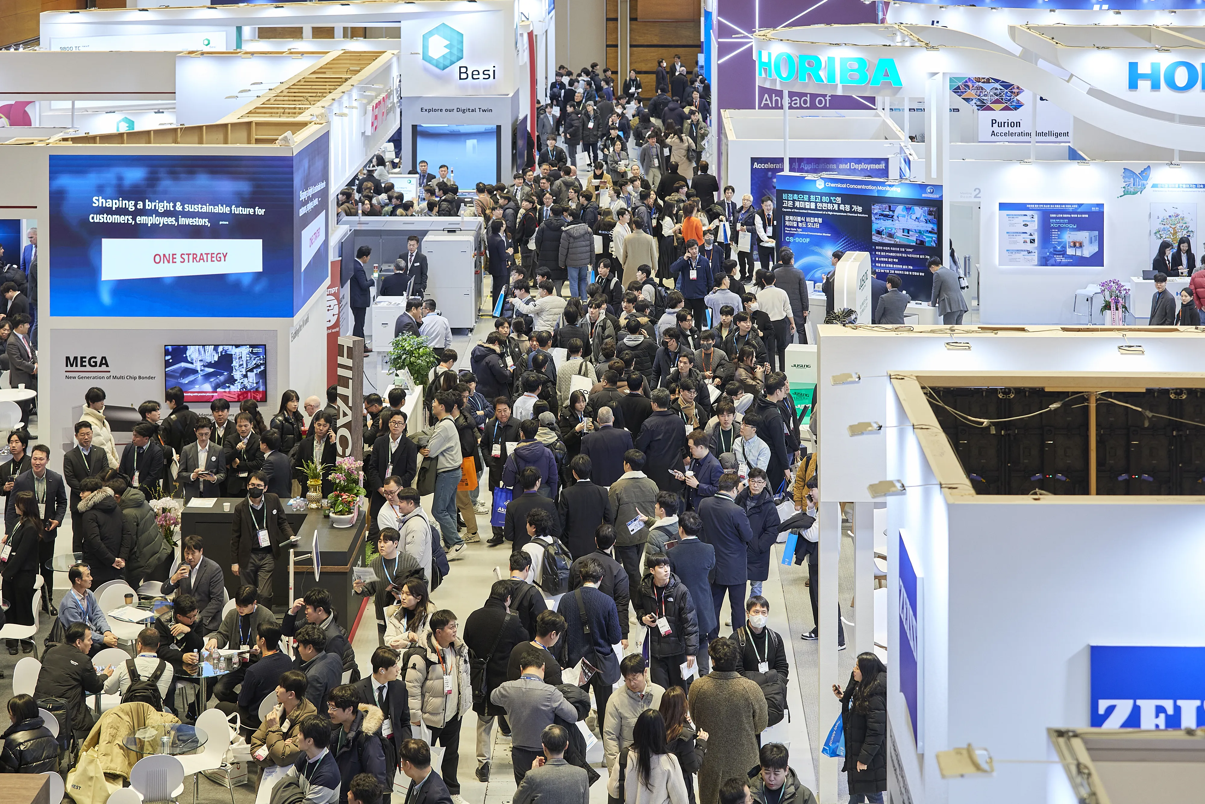
TOKYO ─ October 22, 2024 ─ SEMICON Japan 2024, the largest gathering of leaders from the microelectronics manufacturing supply chain in Japan, will assemble more than 1,000 exhibitors showcasing semiconductor solutions for smart technologiesfrom Dec. 11-13 at Tokyo Big Sight. The event will feature the inaugural Advanced Design Innovation Summit (ADIS), with exhibitions and presentations focusing on next-generation chip design and verification, current challenges, and the future of the industry. SEMICON Japan 2024 will also feature presentations and executive panels on key industry topics with thought leaders from the semiconductor industry ecosystem, academia, and government. Registration is open.
Due to increased registration, the 2024 exhibition is expanding into the Tokyo Big Sight Conference Tower and halls 1-8 of the East Exhibition Hall.
SEMICON Japan 2024 Featured Speakers
Akira Amari, Member of the House of Representatives, Japan
Makiko Eda, Managing Executive Officer, Chief Sustainability Officer, and DEI Officer of Sumitomo Corporation
Dario Gil, Senior Vice President and Director of IBM Research
Tetsuro Higashi, Chairman of the Board of Directors of Rapidus Inc.
Jim Keller, CEO of Tenstorrent
Terushi Shimizu, Representative Director, President and CEO of Sony Semiconductor Solutions
Ho-Young Son, Vice President of Advanced Packaging Development at SK Hynix
Special Exhibits
The AI Summit & Startup will provide a comprehensive overview of AI – from the big picture, down to the latest technologies.
SEMICON Stadium will allow attendees to experience AI’s evolution first-hand by interacting with state-of-the-art robots.
SEMI Technology Pavilions will include a Quantum Computing Pavilion, Power Electronics Pavilion, SEMI Smart Mobility Pavilion, Ministry of the Environment Pavilion, and Disassembly Corner.
More exhibits and details will be announced.
Additional Conference Highlights
Market and advocacy: Government officials, researchers, analysts, and industry specialists will discuss the latest semiconductor market trends. This includes The Challenges to a $1 Trillion Semiconductor Market opening session, Bulls & Bears session presented by Japan's top securities analysts, the Semiconductor Materials Forum, and the SEMI Market Forum.
Sustainability: SEMICON Japan 2024 will include a Sustainability Summit keynote session themed Semiconductors Supporting Global Environmental Conservation and World Economic Growth. In addition, the Sustainability Summit will include sessions on PFAS and greenhouse gases, as well as an additional session on combating climate change for Semiconductor Climate Consortium (SCC) member companies.
Events for future industry leaders: As Generation Z breaks into the semiconductor industry, SEMICON Japan 2024 will feature Yoichi Ochiai's Jyonetsu Lab (Passion Lab), where Ochiai, a media artist, will discuss the future of digitization with students. Additionally, artist, founder, and CEO of Cradle, Sputniko!, will share insights on the active role women play in the semiconductor industry during her presentation, Understand the Importance of DE&I-Equity.
SEMI Global Standards Summit: Innovating Tomorrow: Standards for Future Factories: Advanced packaging, cybersecurity, supply chain, and critical materials need further industry collaboration on standardization. The inaugural SEMI Global Standards Summit aims to identify critical areas and work toward an industry standardization strategy for both a three-year and seven-year timeframe.
Concurrent Events
The Advanced Packaging and Chiplet Summit (APCS) will return to Tokyo Big Sight to assemble top players in semiconductor packaging and board mounting, highlighting the packaging industry’s work to optimize power consumption, reliability, miniaturization, and cost.
FLEX Japan 2024 will create an opportunity for collaboration between product vendors and device and material manufacturers who act as their suppliers. The event will highlight the role of printed electronics for a more sustainable society.
For more details, see the complete seminar schedule or visit the SEMICON Japan 2024 event website.
About SEMI
SEMI® is the global industry association connecting over 3,000 member companies and 1.5 million professionals worldwide across the semiconductor and electronics design and manufacturing supply chain. We accelerate member collaboration on solutions to top industry challenges through Advocacy, Workforce Development, Sustainability, Supply Chain Management and other programs. Our SEMICON® expositions and events, technology communities, standards and market intelligence help advance our members’ business growth and innovations in design, devices, equipment, materials, services and software, enabling smarter, faster, more secure electronics. Visit www.semi.org, contact a regional office, and connect with SEMI on LinkedIn and X to learn more.
Association Contacts
Shuichi Sato/SEMI Japan
Phone: 81.3.3222.5757
Email: [email protected]
Samer Bahou/SEMI Corporate
Phone: 1.408.943.7870
Email: [email protected]
MILPITAS, Calif. – September 3, 2024 – Seeking to bolster global semiconductor value chain efforts to lower greenhouse gas (GHG) emissions, the industry association SEMI released today an analysis by its Energy Collaborative (EC) of current and forecasted low-carbon energy (LCE) markets for Japan, the second in a series of market-specific reports. Developed by the SEMI EC and its sponsors, incorporating insights from the Japanese government and partner organizations, the report outlines policy changes and investments required to increase LCE supply.
 Japan is cited as one of the two most challenging markets for clean energy procurement in the latest annual disclosure report from RE100, a consortium of more than 400 companies committed to using 100% renewable energy. In 2022, LCE made up only 27% of Japan’s electricity generation mix with the remaining 73% covered by fossil fuels. The EC projects the total LCE demand in Japan in 2030 to be 390 to 450 TWh, with the best-case-scenario being that supply falls 20-80 TWh short of demand, providing for only 20%-50% of total voluntary corporate demand.
“The Japan government has goals to revitalize the semiconductor industry and triple global production from JPY 5 trillion now to JPY 15 trillion in 2030,” said Mousumi Bhat, PhD, Vice President, Global Sustainability Programs. “To do so, the industry will need access to LCE to meet its customers’ decarbonization expectations.”
The EC report recommends accelerating the installation of LCE in Japan by:
- Updating land usage policies that enable greater access for LCE development
- Alleviating current policy impediments to facilitate expanding and accelerating offshore wind development
- Overcoming transmission grid bottlenecks with greater clarity on long term grid development plan and implementation / project delivery
- Fostering community collaboration that accelerates designation of LCE promotion zones across the country
- Facilitating collaboration among industries to propagate knowledge of corporate LCE procurement mechanisms.
“The analysis and findings of this substantial body of research provides a strong basis for collaboration with the semiconductor industry, facilitated by the Energy Collaborative’s meetings with government, infrastructure, and other industry leaders,” said Bhat. We provide detailed scenarios of our industry’s needs, energy technology analysis, and the voice of a critical energy customer as the local government plans policies that impact future supply of LCE.”
Each recommendation is supported by detailed analysis of current and historical market conditions in Japan and draws from concrete examples of how other regions have successfully implemented similar measures to drive LCE adoption.
The Energy Collaborative report Key Challenges and Potential Solutions for Expansion and Procurement of Low-Carbon Electricity on Japan is the second of five, joining the report on South Korea. The EC will also analyze Taiwan, Malaysia and Singapore. Organizations sponsoring the EC will get access to more detailed analysis of each region. More information on the benefits of membership and sponsoring the Energy Collaborative initiative is available by contacting Jamie Belliveau at [email protected].
About the Energy Collaborative
The SEMI Energy Collaborative is dedicated to engaging a leadership network of corporations and domain experts to accelerate the pace of adoption of renewable energy solutions together with regional governments and regulators in key markets. Through collaboration with the semiconductor value chain, the EC aspires to improve the currently untenable trajectory of semiconductor manufacturing emissions. Companies sharing this vision from across the semiconductor and energy ecosystems sponsor the EC, along with partners from civil society and non-profit organizations.
About SEMI
SEMI ® is the global industry association connecting over 3,000 member companies and 1.5 million professionals worldwide across the semiconductor and electronics design and manufacturing supply chain. We accelerate member collaboration on solutions to top industry challenges through Advocacy, Workforce Development, Sustainability, Supply Chain Management and other programs. Our SEMICON® expositions and events, technology communities, standards and market intelligence help advance our members’ business growth and innovations in design, devices, equipment, materials, services and software, enabling smarter, faster, more secure electronics. Visit www.semi.org , contact a regional office, and connect with SEMI on LinkedIn and X to learn more.
Association Contact
Samer Bahou
Phone: 1.408.943.7870
Email: [email protected]