downloadGroupGroupnoun_press release_995423_000000 copyGroupnoun_Feed_96767_000000Group 19noun_pictures_1817522_000000Member company iconResource item iconStore item iconGroup 19Group 19noun_Photo_2085192_000000 Copynoun_presentation_2096081_000000Group 19Group Copy 7noun_webinar_692730_000000Path
Skip to main content
Default Banner Image

SEMI News

MILPITAS, Calif. – December 4, 2020 – SEMI, the industry association serving the global electronics design and manufacturing supply chain, today released the following statement from president and CEO Ajit Manocha on the Fiscal Year 2021 National Defense Authorization Act.

semi logo

“SEMI supports the provisions included in the conference report on the Fiscal Year 2021 National Defense Authorization Act for programs to provide incentives for microelectronics manufacturing and research in the U.S. They are helpful steps to support microelectronics innovation and manufacturing. SEMI thanks Sens. Cornyn, Warner, Cotton and Schumer, Reps. Matsui and McCaul, and other congressional and administration leaders for their support and hard work to enact these provisions. We look forward to working with Congress and the administration to provide the funding needed to implement these programs and to enact the CHIPS Act investment tax credit which will provide the certainty needed to attract many more new, large-scale microelectronics manufacturing investments in the U.S.”

About SEMI

SEMI® connects more than 2,400 member companies and 1.3 million professionals worldwide to advance the technology and business of electronics design and manufacturing. SEMI members are responsible for the innovations in materials, design, equipment, software, devices, and services that enable smarter, faster, more powerful, and more affordable electronic products. Electronic System Design Alliance (ESD Alliance), FlexTech, the Fab Owners Alliance (FOA) and the MEMS & Sensors Industry Group (MSIG) are SEMI Strategic Association Partners, defined communities within SEMI focused on specific technologies. Visit www.semi.org to learn more, contact one of our worldwide offices, and connect with SEMI on LinkedIn and Twitter.

Association Contact
Samer Bahou/SEMI
Phone: 1.408.943.7870
Email: [email protected]  

MILPITAS, Calif. – December 2, 2020 – Global semiconductor equipment billings surged 30% year-over-year and rose 16% to US$19.4 billion from the prior quarter, SEMI announced today in its Worldwide Semiconductor Equipment Market Statistics (WWSEMS) Report.

semi logo

SEMI and the Semiconductor Equipment Association of Japan (SEAJ) gather the data from more 80 global equipment companies that provide monthly reports. Following are quarterly billings data in billions of U.S. dollars quarter-over-quarter and year-over-year change by region:


Region

Q32020

Q22020

Q32019

3Q2020/2Q2020

3Q2020/3Q2019

China

5.62

4.59

 3.44

23%

63%

Taiwan

4.75

3.51

 3.90

36%

22%

Korea

4.22

4.48

 2.20

-6%

92%

Japan

2.24

1.72

 1.67

30%

34%

North America

1.37

1.64

 2.49

-17%

-45%

Rest of the World

0.60

0.37

 0.76

64%

-21%

Europe

0.58

0.46

 0.39

25%

47%

Total

 19.38

 16.77

 14.86

16%

30%

Source: SEMI (www.semi.org) and  SEAJ (www.seaj.or.jp), December 2020


The SEMI Equipment Market Data Subscription (EMDS) provides comprehensive market data for the global semiconductor equipment market. A subscription includes three reports:

  • Monthly SEMI Billings Report, a perspective on equipment market trends
  • Monthly Worldwide Semiconductor Equipment Market Statistics (WWSEMS), a detailed report of semiconductor equipment billings for seven regions and 24 market segments
  • SEMI Semiconductor Equipment Forecast, an outlook for the semiconductor equipment market.

For more information or to subscribe, please contact the SEMI Industry Research and Statistics Group at [email protected]. More information is also available online.

About SEMI
SEMI® connects more than 2,400 member companies and 1.3 million professionals worldwide to advance  the technology and business of electronics design and manufacturing. SEMI members are responsible for the innovations in materials, design, equipment, software, devices, and services that enable smarter, faster, more powerful, and more affordable electronic products. Electronic System Design Alliance (ESD Alliance), FlexTech, the Fab Owners Alliance (FOA) and the MEMS & Sensors Industry Group (MSIG) are SEMI Strategic Technology Communities, defined communities within SEMI focused on specific technologies. Visit www.semi.org to learn more, contact one of our worldwide offices, and connect with SEMI on LinkedIn and Twitter.

Association Contact
Michael Hall/SEMI
Phone: 1.408.943.7988
Email: [email protected]


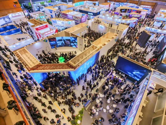
As the global semiconductor industry enters a decisive new phase shaped by artificial intelligence, SEMICON Korea 2026 convened the ecosystem from February 11–13 in Seoul, bringing together the companies, technologies, and talent required to sustain momentum on both sides of the AI equation: using AI to transform semiconductor operations, and advancing semiconductor innovation to enable the next generation of AI systems.At the SEMICON Korea press conference, Hyun Cha, President, SEMI Korea stated that with nearly 550 exhibiting companies and over 2,400 booths, the event underscored how progress now depends on a virtuous cycle of collaboration across the entire value chain—from materials and equipment to design, manufacturing, packaging, and systems integration.Opening Perspectives: Collaboration as the Catalyst In the opening ceremony, Ajit Manocha, President and CEO of SEMI, framed the opportunity and challenge ahead: AI is accelerating the industry’s trajectory toward a trillion-dollar market, but sustaining that growth will require deeper collaboration across an increasingly complex ecosystem.That message was reinforced by YH Lee, Chairman of Wonik, who emphasized the need for alignment across the value chain, “looking side to side, not only forward,” as scaling semiconductor technologies grows more difficult. From a policy perspective, Shinhak Moon, Vice Minister of Korea’s Ministry of Trade, Industry Resources (MOTIR), highlighted the importance of the full ecosystem, including parts, materials, and equipment, while cautioning that resilience will be critical amid economic cycles. Together, these perspectives set the stage for a keynote program focused on how AI and semiconductors are now co-evolving.Opening Keynote: Samsung Electronics on Architecting the Future of AI SystemsThe keynote program opened with Jaihyuk Song, Corporate President and CTO of Samsung Electronics, who examined what comes next for AI systems as compute and memory demands rise exponentially. He described a widening gap between compute performance and memory bandwidth, positioning advanced packaging and architectural innovation as central to closing that gap.Song outlined Samsung’s focus on next-generation memory technologies, including high-bandwidth memory and compute-in-memory approaches, as well as the transition beyond traditional Moore’s Law scaling toward planar, vertical, and stacked architectures. His message was clear: sustaining AI performance gains will depend on tight integration across design, process technology, packaging, and system architecture, reinforcing the need for ecosystem-wide coordination. ASE: From Chip Integration to System OptimizationTien Wu, CEO of ASE, expanded the discussion from devices to systems, arguing that advanced packaging has become a primary driver of system-level performance and efficiency. As AI workloads push power, thermal, and bandwidth limits, Wu described a shift from single-chip packages toward heterogeneous integration, 2.5D and 3D architectures, and co-packaged optics.Wu emphasized that productivity, yield, and throughput will increasingly determine competitiveness as packages grow larger and more complex. His perspective reinforced a central theme of SEMICON Korea 2026: AI-driven demand is forcing tighter coupling between design, manufacturing, and packaging, making collaboration not optional, but essential.Cadence: AI-Enabled Design Across the Value ChainBoyd Phelps, Senior Vice President and General Manager of Silicon Solutions at Cadence Design Systems, highlighted how AI is already reshaping semiconductor design and development. As process scaling slows and cost per transistor rises, Phelps described disaggregation and chiplets as a new abstraction layer that enables continued innovation through customization and configurability.He also pointed to the growing role of AI-driven design automation, noting that a significant portion of recent designs leveraged AI-enabled tools. Cadence’s end-to-end portfolio—from IP and tools to packaging and test—illustrated how AI is becoming both a design accelerant and a necessary response to rising system complexity, reinforcing the industry’s virtuous cycle.Lam Research: Velocity Through AI and AutomationThe theme of operational transformation took center stage with Tim Archer, President and CEO of Lam Research, who introduced “velocity” as the defining imperative of the AI era. As AI-driven demand accelerates product cycles and increases complexity, Archer argued that speed must be matched with direction—enabled by AI, automation, and digital twins.Archer detailed Lam’s progress toward autonomous fabs, equipment intelligence, and collaborative virtual development environments that reduce variability and accelerate process development. These capabilities, he explained, allow the industry to respond faster while preserving quality and resilience—another example of AI improving semiconductor operations even as semiconductor innovation enables AI growth.SK hynix: AI as a Tool for Memory InnovationLooking further into the future, Sunghoon Lee, Senior Vice President and Head of R D Process at SK hynix, addressed the mounting difficulty of sustaining memory technology cadence. As stacking, bonding, and material challenges intensify, Lee described a shift toward AI-based R D models that dramatically accelerate material discovery and optimization.By integrating AI into material exploration and process development, SK hynix is shortening development cycles and enabling new memory architectures. Lee emphasized that realizing the full potential of AI-driven R D will require greater data sharing and collaboration across partners—reinforcing the ecosystem-wide virtuous cycle.NVIDIA: From Chips to AI InfrastructureThe final keynote, delivered by Soyoung Jeong, Head of Korea Business at NVIDIA, framed the transformation of NVIDIA from a GPU company into an AI infrastructure provider. He described how accelerated computing and AI factories are reshaping chip design, manufacturing, packaging, and system integration.From AI-assisted design and simulation to system-level optimization and physical AI, NVIDIA’s approach illustrated how semiconductors and AI are now inseparable, each advancing through the other. Partnerships across memory, equipment, and software ecosystems were highlighted as critical to sustaining this momentum.A Program Aligned Around the Same ThemeBeyond the keynotes, SEMICON Korea 2026 reinforced these messages through technology symposia, AI and smart manufacturing forums, cybersecurity discussions, and workforce development initiatives—all focused on enabling AI-powered innovation across the semiconductor lifecycle.Additional Program Highlights: Extending the Virtuous Cycle Across the EcosystemBeyond the keynote stage, SEMICON Korea 2026 reinforced the same virtuous cycle of AI and semiconductor innovation through a wide range of technical, business, and workforce programs designed to engage every layer of the value chain.AI Summit: Translating Strategy into Industrial ImpactThe AI Summit, co‑hosted by SEMI and KAIST, served as a focal point for aligning academic research, device manufacturers, and equipment leaders around AI-powered industrial innovation. Featuring faculty from KAIST alongside representatives from Samsung Electronics, SK hynix, and global equipment companies, the summit explored technology strategies and future roadmaps aimed at accelerating AI adoption across semiconductor manufacturing and design.The discussions reinforced a central theme of SEMICON Korea 2026: AI is no longer an isolated software layer, but a system-level capability that must be embedded across processes, tools, and infrastructure to unlock its full value.Smart Manufacturing Forum: Advancing the Autonomous FabThe Smart Manufacturing Forum highlighted how AI, digital twins, and real-time data are transforming semiconductor fabs toward more autonomous, resilient operations. Speakers shared trends and success cases demonstrating how advanced analytics and AI-driven decision-making are improving yield, productivity, and operational agility.This forum echoed themes raised by equipment and manufacturing leaders in the keynote program, underscoring how AI-driven manufacturing excellence is becoming a prerequisite for meeting the speed, scale, and quality demands of next-generation AI chips.Startup Summit: Fueling Innovation from the Ground UpThe Startup Summit showcased emerging semiconductor and display startups focused on applying AI to improve chip performance, energy efficiency, and manufacturing processes. By connecting startups with industry leaders and venture capital firms—including Applied Ventures, Intel Capital, Samsung Ventures, and SK hynix—the summit emphasized the importance of nurturing innovation across the ecosystem.These early-stage technologies represent the next wave of ideas feeding into the virtuous cycle, where AI-enabled innovation at the startup level can scale rapidly through collaboration with established players.Cybersecurity Forum: Securing the AI-Driven Semiconductor FutureAs AI becomes deeply embedded in semiconductor operations and data flows, the Cybersecurity Forum addressed the growing need for digital trust across the ecosystem. Global experts examined cybersecurity challenges related to compliance, fab security, and AI data governance, highlighting the importance of collaboration to protect sensitive data and intellectual property.The forum reinforced that secure, trusted infrastructure is a foundational requirement for the AI-driven transformation discussed throughout SEMICON Korea 2026.Conclusion: Advancing TogetherSEMICON Korea 2026 made clear that the next phase of industry growth will not be driven by isolated breakthroughs, but by a virtuous cycle of alignment across the full semiconductor value chain. By integrating AI into design, manufacturing, and operations—and by advancing semiconductor technologies that power AI—the industry is building a foundation for sustained innovation. As the event demonstrated, progress will be fastest when the ecosystem moves forward together.Samer Bahou is Director, Corporate Communications at SEMI. Jaegwan Shim is Senior Specialist, Marketing at SEMI Korea.
Read More

Date: November 13, 2025 Location: San Jose, California

yieldWerx, a leading provider of end-to-end semiconductor test data and yield analytics, today announced a strategic collaboration with iTest, a premier independent IC testing laboratory based in Silicon Valley. This partnership integrates yieldWerx’s enterprise-grade analytics platform directly into iTest’s production environment, enabling customers to access advanced data visualization, AI-powered analytics, and automated workflows—right from within the test lab, eliminating the need for complex integrations or data transfers.

The collaboration bridges a long-standing gap between test execution and data intelligence. By combining iTest’s high-performance testing capabilities with yieldWerx’s unified analytics engine, semiconductor customers will benefit from:

  • Real-Time Insights at the Source: Access dashboards, correlation analytics, and SPC control directly within iTest’s secure lab environment.
  • Accelerated Engineering Feedback: Automated lot dispositioning and outlier detection speed up yield learning and process optimization.
  • Remote Data Access & Collaboration: Engineers can securely access test data from their offices to support product engineering and test program development.
  • Faster Time-to-Market: Enterprise-grade analytics that once took months to implement are now available within days.
  • Enhanced Collaboration & Transparency: OEMs, fabless companies, and foundries gain shared visibility across data silos, improving decision-making and accountability.
  • Upskilling Opportunities: iTest customers can leverage industry-standard tools and methodologies, reducing the need to reinvent analytics processes.

    About yieldWerx

    yieldWerx’s platform unifies heterogeneous data across wafer sort, final test, and assembly into a centralized repository, offering AI-driven pattern analysis, adaptive limit setting, and root-cause correlation across product lines and sites. More importantly, it allows iTest customers to perform correlation, characterization, and Gage R&R Analysis.

    About iTest

    iTest operates one of North America’s most advanced semiconductor test facilities, equipped with ultra– high-density configurations and cutting-edge automated test systems for digital, high pin-count, and HPC/AI devices.

    Statements from Leadership

    “This collaboration marks a new era in operationalizing advanced test data analytics within leading test labs,” said Aftkhar Aslam, CEO of yieldWerx. “By embedding our platform into iTest’s environment, customers gain immediate, secure access to analytics that previously took months to deploy—reducing decision latency, lowering risk, and accelerating time-to-market.”

    “Partnering with yieldWerx enhances iTest’s service offering by delivering actionable intelligence alongside world-class testing,” said Rabbi Islam, CEO of iTest. “Together, we’re giving customers a faster path from data to decisions.”

    For further information, please visit https://www.yieldWerx.com or https://www.iTestinc.com/.

The Challenge

Ayar Labs’ engineering teams faced challenges ingesting and analyzing non-standard test data across electro-optical and final test flows while scaling to meet aggressive go-to-market timelines. They sought a test analytics partner capable of loading, validating, and extracting insights from diverse datasets while supporting real-time alerting, yield recovery, and deep engineering analytics.

The Implementation

Week 1–2: Connecting the Pipes

Within the first two weeks, a secure cloud instance of yieldWerx was deployed, and raw data files were streaming in. The platform’s flexible pipelines ingested test data without custom code. The yieldWerx team went further, helping refine business rules, improve data quality, and enrich the information for greater downstream impact.

Week 3: First Insights

By week three, live dashboards were operational. Engineers could view wafer maps, outlier signatures, and correlations that previously required manual effort and scripting. Instead of working across multiple spreadsheets, they now had traceable, drill-down analytics at their fingertips.

Week 4: Real Results

In less than a month, the system was already supporting real yield decisions. Lots that previously required lengthy reviews were dispositioned in hours. Engineers trusted the analytics, and leadership recognized the tangible impact on quality and time-to-market. Ayar Labs is now preparing to onboard additional data formats, including qualification, reliability, and characterization.

The Outcome

The 30-Day Challenge demonstrated that yieldWerx is not just another analytics solution. In weeks, not months, yieldWerx moved from fragmented data to a unified platform that drives yield improvement, accelerates ramps, and reduces risk.

About yieldWerx

yieldWerx, an industry leader in semiconductor yield management, provides a platform that enables manufacturers to collect, validate, and act on production data across the entire semiconductor manufacturing lifecycle.

About Ayar Labs

Ayar Labs, a leader in optical engines for co-packaged optics, is transforming AI infrastructure by accelerating data movement in scale-up networks. Its industry-first optical I/O solution enables customers to maximize compute efficiency and performance while reducing costs, latency, and power consumption. Based on open standards and optimized for AI training and inference, Ayar Labs’ optical interconnect solutions are backed by a robust ecosystem to easily integrate into AI systems at scale. Ayar Labs was founded in 2015 and is funded by domestic and international venture capital firms, as well as strategic investors including AMD, Applied Ventures, GlobalFoundries, Hewlett Packard Pathfinder, Intel Capital, and NVIDIA.

Statements from Leadership

“Our collaboration with yieldWerx gave us measurable results in just 30 days. Their platform ingested
our complex photonics data, and the insights have accelerated how we make yield and quality decisions.”

— Garth Thompson, CIO, Ayar Labs

“Partnering with Ayar Labs has been both inspiring and validating. Photonics test data is some of the most complex in the industry, spanning electrical, optical, and multi-dimensional signatures that traditionally take months to integrate. Delivering measurable results in just 30 days shows the power of a unified, modern analytics platform. We’re proud that yieldWerx is helping Ayar Labs accelerate their roadmap, improve yields, and bring truly groundbreaking optical I/O technology to market faster and with higher confidence. “

— Aftkhar Aslam, CEO, yieldWerx
For further information, please visit https://www.yieldWerx.com or https://ayarlabs.com/.

As Europe’s microelectronics industry enters a new era of growth, one question stands out: do we have the talent pipeline to match our ambitions? The European Chips Skills Academy (ECSA), coordinated by SEMI Europe, is addressing this challenge through coordinated action, insightful research, and strong collaboration between industry and academia. Why Talent and Skills Matter The semiconductor sector in Europe is undergoing rapid transformation, driven by the European Chips Act and large-scale investments in design, manufacturing, and packaging. This momentum creates significant demand for engineers, technicians, and specialists across the electronics value chain.However, Europe faces a growing structural challenge. An ageing workforce, modest growth in technical graduates, and limited public awareness of semiconductor careers are widening the talent gap.The ECSA Skills Strategy 2024, published in November 2024, provides a detailed overview of this situation. The updated Skills Strategy 2025, released in November 2025, reinforces the urgency with new data and recommendations.According to the latest report, around 30% of Europe’s current semiconductor workforce will retire by 2030, while the inflow of graduates is increasing by less than 1% per year. This creates an annual shortfall of approximately 10,800 skilled professionals across the European value chain. Read the full report, available to download on the ECSA website.Without decisive action, this shortfall could limit Europe’s ability to meet its strategic goals in semiconductors, electronics, and digital technologies.What is European Chips Skills Academy (ECSA)?ECSA connects industry, academia, training providers, and policymakers to create a sustainable and inclusive skills ecosystem for the electronic components and systems (ECS) sector.Its core objectives are:To attract new talent into semiconductor and ECS careers.To upskill and reskill professionals for emerging roles.To build a long-term, future-ready talent pipeline across Europe.Through this initiative, SEMI Europe is leading the conversation on talent and skills, turning awareness into action and strategy into measurable results.Key ECSA Initiatives:1. ECS Summer School The annual ECS Summer School invites STEM students from across Europe to explore careers in microelectronics through lectures, workshops, and hands-on learning.The 2024 edition took place in Bertinoro, Italy, while the 2025 edition was hosted by the Budapest University of Technology and Economics in August 2025, under the theme “Fascinating Electronics for a Cool World.”The 2026 edition will return to Bertinoro, Italy on August 23-26. These events give students a first-hand look at the semiconductor ecosystem, helping them connect with experts and understand how their studies translate into real-world careers.Read more about the 2025 Summer School.2. “Day in a Fab” WebinarsThe “Day in a Fab” series offers students and young professionals the opportunity to interact directly with experts from semiconductor fabs, design houses, and equipment manufacturers.These webinars provide practical insights into various career paths within the ECS industry, helping participants better understand the range of opportunities beyond traditional engineering roles.By bridging the gap between academia and industry, these sessions help students envision a future within the European semiconductor ecosystem.See upcoming events on the ECSA website.3. Skills Strategy ReportsECSA’s Skills Strategy Reports (2024 and 2025) form the backbone of Europe’s talent development roadmap.They provide:Quantitative forecasts of job demand, workforce needs, and potential skill shortages.Insights from over 130 industry and academic experts.Recommendations for training, mobility, and reskilling programmes.The 2024 Skills Strategy Report can be accessed here, while the 2025 update is available here.These reports help policymakers, companies, and educators align their efforts to strengthen Europe’s competitiveness and ensure a resilient talent ecosystem.SEMI Europe’s Leadership in Talent and SkillsAs the global industry association for electronics manufacturing and design, SEMI Europe plays a central role in addressing the talent challenge.Through ECSA, SEMI Europe:Validates industry needs to ensure training and education are aligned with real-world demand.Connects universities and training providers with semiconductor companies to co-develop curricula.Promotes visibility and inclusion across the ECS community.Supports mobility and collaboration to create a Europe-wide approach to skills development.This leadership transforms the skills agenda from a background issue into a strategic pillar of Europe’s semiconductor ecosystem.Looking AheadThe European semiconductor industry is entering a decisive decade. The technology and investment potential are enormous, but they depend on a skilled and motivated workforce.ECSA’s work from the Skills Strategy reports to the Summer School and student engagement activities is creating a structured, evidence-based approach to developing that workforce.The path forward is clear: attract, train, and empower the next generation of engineers and innovators. With SEMI Europe’s guidance, the European Chips Skills Academy is ensuring that Europe’s ambitions in chips and microelectronics are matched by the people who will make them possible.The European Chips Skills Academy (ECSA) is a pan-European initiative coordinated by SEMI Europe and co-funded by the European Education and Culture Executive Agency (EACEA) under project number 101110124.Learn more about ECSA’s mission.SEMI ContactJatin Mendiratta, Communication CoordinatorEmail: [email protected]
Read More
This year’s SEMICON West brought together industry experts from around the world to share insights on three of today’s most pressing topics: geopolitics, sustainability, and the semiconductor supply chain. From October 7-8, leaders from each field offered updates during SEMICON West’s Executive Panel Series, with each topic explored in its own hour-long session.Strategic Silicon: Geopolitics Shaping the Future of Semiconductors SEMICON West’s Executive Panel Series began on Tuesday, October 7, with a discussion on today’s geopolitical ecosystem and its impact on the semiconductor industry. Speakers compared the U.S. semiconductor landscape with China’s, highlighted supply chain strategies to mitigate disruption, and defined what it means to “win” the AI race. Mackenzie Hawkins from Bloomberg News moderated the panel, which featured Vince Jesaitis from Arm, Frank Heemskerk from ASML, Olivier Blachier from Entegris, Sarah Kemp from Intel, and Rich Ashooh from Lam Research.First, the panelists mentioned the U.S. CHIPS Act and the legislation’s attempt to diversify the semiconductor supply chain. Jesaitis added that countries are prioritizing supply chain resiliency, to which Kemp pointed to rising customer willingness to pay premiums for stronger supply chains. But what does it take to strengthen a supply chain? According to the panelists, a prevailing approach has been to regionalize operations. More regionalized supply chains can better withstand policy changes overall, but Ashooh noted that government regulations often can’t keep pace with innovation demands. China, in particular, may have key advantages in this respect. “The U.S. remains the most innovative environment in the world,” said Ashooh. “But if the Chinese government declared something a priority, the support will be there for it.” He also mentioned this arrangement allows China to advance in spurts.Kemp also stated that even with U.S. innovation and government incentives, the country faces longer construction times and greater policy complexity. Meanwhile, China is doubling down on its industry with resources and clear intent. Ashooh also added that China has more leverage in 2025 than it did during the first Trump administration. To address this, the panel recommended policy refinement to make U.S. trade relations more seamless. Furthermore, Heemskerk stated that the best government policies are often boring, advising governments to be predictable and reliable.The discussion concluded with mention of the AI race. Amidst discussion about what it means to “win,” Ashooh offered a simple explanation. Winning, he said, is seeing only customers in front of you instead of competitors. Sustainability Panel: Path to Success—The Semiconductor Industry Leads the WayAfter the Geopolitics panel, the stage swiftly transitioned to a new discussion centered on sustainability. Speakers included Elena Kocherovsky from Applied Materials, Beth Elroy from Micron, Joshua Kang from Qualcomm, and Sanchali Bhattacharjee from Google. SEMI’s Mousumi Bhat moderated this session.It may come as no surprise to learn that sustainability is reaching a critical juncture. According to the Climate Clock, the world has just under four years to address climate change before it becomes irreversible. Bhat pointed to this figure, emphasizing the mounting importance of industry-wide collaboration to make a tangible difference. With such a tight window for change, the panelists explained what’s being done to address these issues. Using AI to strengthen climate data, for example, came up several times. For instance, Sanchali mentioned that AI can bring in new data parameters to solve issues much faster. “We’re sitting at an inflection point where we have to harness the power of data,” she said.Elroy also shared opportunities to replace aging infrastructure with more sustainable equipment, as well as creating products that consume less energy from the start. However, distraction from climate goals is still a significant risk. Kocherovsky highlighted the industry’s limited resources, underscoring the importance of allocating them to efforts that move the needle. She cited clean energy adoption, noting that 80% of the industry’s emissions come from electricity. Fortunately, mitigation efforts are underway. Kang pointed to Qualcomm’s sponsorship of AI-powered air quality monitoring devices in Thailand, while Kocherovsky also touched on Applied Materials’ new sustainability projects. These efforts, while substantial, are nowhere near exhaustive. Tangible work is being done across the entire semiconductor ecosystem to make its solutions more sustainable, but it’s only the beginning. Charting the Course: Futureproofing Your Supply ChainsAs supply chain security has risen in priority, Wednesday’s panel detailed the industry’s efforts to strengthen it. Although COVID-19 exposed the urgent need for more resilient semiconductor supply chains, core issues have existed long before then. To explore this topic, I engaged speakers from across the value chain, including EMD’s Steven Johnston, AltaScient’s Rekha Menon-Varma, GlobalFoundries’ Roger Kao, Polar Semiconductor’s Surya Iyer, and Cisco’s Aman Aflaki. Today’s supply chain risks are enormous. From geopolitical tensions to natural disasters and cybersecurity threats, the semiconductor supply chain must withstand several intense and ongoing conditions. Because of this, the panel stressed the importance of early warning awareness and building buffers to counter setbacks. Creating buffers, Aflaki said, leads to necessary redundancies like using digital twins when feasible or engaging with second-and third-tier suppliers. Today’s customers, he said, also tend to be more focused on resilience and risk management rather than cost. Another emerging risk management solution is to use AI to build scenario models before incidents happen. As AI technology advances, companies that adopt it sooner rather than later could gain a competitive advantage. Johnston also added that AI could lead to more efficient R D and material sourcing. In addition, the panel pointed to the growing worldwide shift to regionalize supply chains. Menon-Varma highlighted that each country is approaching this in its own way, with many new global partnerships arising due to U.S. tariffs and export controls. Kao also reinforced today’s “local-for-local” supply chain trend.Finally, the panel ended with a discussion on collaboration. Although most leaders cite collaboration as crucial for the industry’s future, Johnston noted that working together is often halted by IP concerns. To address this, Iyer pointed to organizations like SEMI that unite key players to solve industry-wide problems.SEMI would like to thank all speakers, sponsors, and attendees for the success of this year’s Executive Panel Series. Bettina Weiss is Chief of Staff Corporate Strategy at SEMI.
Read More
The Rising Stars: 20 Under 30 blog series celebrates the brightest young leaders shaping the future of the semiconductor industry. These exceptional individuals have earned the SEMI Europe 20 Under 30 Award for making a remarkable impact across the supply chain—whether in engineering, sales, marketing, or R D. Nominations for the 2025 20 Under 30 Award are now open, providing the opportunity to recognize and honor the next wave of industry trailblazers.The series spotlights these rising stars for their career achievements, commitment to innovation, leadership skills, and dedication to driving both business success and community growth.Follow their inspiring journeys and discover how they are thriving and paving the way for future generations in the semiconductor world.Meet Anne-Mary Yeboah, Technology Manager at SoitecWith a background in materials science and a strong interest in technology, Anne-Mary Yeboah has built a career that connects the worlds of engineering and management. After earning her degree in engineering, she deepened her understanding of business through a Specialized Master’s in Management—an experience that broadened her perspective and prepared her for the challenges of a global, fast-moving industry.Today, as Technology Manager at Soitec, Yeboah leads projects that contribute to the next generation of semiconductor innovations. Her journey reflects a balance of technical curiosity, leadership growth, and a belief in the power of inclusion. In this interview, she shares her thoughts on career development, the importance of diversity, and how young professionals can find their voice in a rapidly evolving industry.SEMI: What inspired you to join the semiconductor industry? Yeboah: I’ve always been fascinated by technology, and semiconductors are at the core of innovation today. They are everywhere, from smartphones to electric vehicles, and being part of this field means contributing directly to the technologies shaping our lives and future.SEMI: How did your early experiences and education shape your career path?Yeboah: My engineering studies led me to specialize in materials science, which naturally included semiconductors. Later, I decided to expand my knowledge by pursuing a Specialized Master’s in Management. This combination of technical and business perspectives shaped my career path and ultimately brought me to Soitec, where I now connect both worlds as a Technology Manager.SEMI: Can you share a professional accomplishment you’re most proud of, and explain why it’s significant to you?Yeboah: I’m especially proud of starting my career directly as a Technology Manager. This role has allowed me to contribute to complex, strategic projects and collaborate with teams across functions. Working on products that will drive future innovations is deeply fulfilling and gives meaning to my work every day.SEMI: As a young professional in the industry, what is your greatest challenge? Yeboah: One of the biggest challenges has been finding my voice in a highly experienced environment. It can be intimidating at first, but I’ve learned to turn it into an opportunity to ask questions, learn quickly, and build confidence in my contributions. It has pushed me to develop a broad skill set and become an effective collaborator across teams.SEMI: What advice would you give to younger generations aspiring to make an impact in this industry?Yeboah: Dare to step forward and don’t create your own limits. Ask questions, even when you’re surrounded by experts, curiosity is a strength. Also, be patient. Building credibility and seeing your impact takes time, but each experience helps you grow and move closer to your goals.SEMI: How do you envision future work environments?Yeboah: I see the workplaces of the future as more innovative, inclusive, and collaborative. Diversity should be central, everyone should feel that their voice and perspective matter. At Soitec, initiatives like Women@Soitec are great examples of how gender equality and inclusion can empower people to thrive. I also believe technology and flexibility will continue to reshape how we work, helping us achieve both high performance and balance.SEMI: What impact has the 20 Under 30 Award had on your career? Yeboah: Receiving the 20 Under 30 Award has been a true honor and a wonderful source of motivation. It gave me a moment to reflect on how far I’ve come and to feel proud of my journey. The recognition has boosted my confidence, increased my visibility, and encouraged me to continue pushing forward in my career.Following 20 Under 30 JourneysAnne-Mary Yeboah’s story highlights the determination and adaptability driving today’s new generation of semiconductor professionals. Her ability to bridge science and management reflects the diverse skill sets shaping the industry’s future.The Rising Stars: 20 Under 30 blog series celebrates the exceptional talent and leadership driving the future of the semiconductor industry. Each of the young innovators honored is excelling in their respective fields while shaping the landscape of technology and business with their visionary approaches and dedication. Their stories exemplify the remarkable achievements and unwavering commitment that define the next generation of industry leaders. The series is intended to inspire and motivate future professionals to pursue their passions and embrace the opportunities within this dynamic industry. Stay tuned for more stories of rising stars who are paving the way for continued growth and innovation in the semiconductor world.Learn more about the SEMI Europe 20 Under 30 Award and the recipients honored at SEMICON Europa. SEMI ContactJames Lam, Business Development ManagerEmail: [email protected]
Read More
Every November, the U.S. pauses to honor those who have served our nation—the men and women whose dedication, discipline, and teamwork have safeguarded our freedom. The best way to thank veterans is not just with words. It’s with action.In the semiconductor industry, that action means creating pathways for veterans to build meaningful civilian careers where their skills, experience, and values are not only recognized, but celebrated. Through SEMI Foundation’s VetWorks initiative, companies across the industry are doing just that, working together to raise awareness, share best practices, and open doors for the military community.Through VetWorks, SEMI is proud to help veterans find new purpose in powering the technologies of tomorrow. And as more employers recognize the unmatched value of veteran talent, the industry will continue to grow stronger technically, strategically, and culturally.Why Veterans and Semiconductors Are a Natural MatchVeterans bring the kind of precision, accountability, and technical excellence that drive the semiconductor industry forward. From operating complex systems to leading diverse teams under pressure, veterans possess the same qualities that make this industry thrive.Kathy Garner, Director of Talent Acquisition at TEL (Tokyo Electron), notes:“Veterans are well-versed in cutting-edge technology. Today’s military is high-tech, state-of-the-art, and computer-based. Veterans are uniquely matched to our industry as their jobs are highly technical and safety-conscious; they appreciate guidelines, follow directions, and possess a strong sense of team.”This alignment of skills and culture makes veterans not just excellent employees, but invaluable contributors to the semiconductor industry’s mission of powering innovation and national competitiveness.Turning Appreciation into OpportunityAcross the VetWorks Employer Group, companies are transforming gratitude into action by recruiting, training, and supporting veterans and reservists as they transition to civilian careers.“I participate in VetWorks because I believe the brave men and women of our military deserve support and opportunities if they choose to enter the civilian workforce,” said Katie Maloney, Business Line Manager at Edwards Vacuum. “They have sacrificed for our country, and we can help connect them to a rewarding career in the semiconductor industry. This transition is often stressful for military members and their families, despite the fact that veterans are ideally suited for the many roles our industry needs to fill. As a Navy veteran, participation is a small way for me to pay it forward.”“The semiconductor industry is full of veterans,” said Curtis Geroy, Manager of Military Talent Acquisition at Applied Materials and a U.S. Navy Reserve Officer. “Serving as a reservist and having leaders who understand my commitment to duty gives me the extra support needed to meet my reserve obligations.”These stories reflect what’s possible when companies don’t just honor veterans but invest in helping them translate their service into purposeful, future-ready careers.An Industry-Wide EffortMany leading employers are already stepping up and partnering through SEMI VetWorks, including Applied Materials, ASM, ASML, Edwards Vacuum, EMD Electronics, Entegris, KLA, Lam Research, Micron, Polar Semiconductor, TEL, TSMC, and Western Digital, among others.Together, they form a growing network of organizations committed to building awareness within the military community, connecting veterans to open roles, and ensuring every company in the semiconductor ecosystem is ready to support them.Through joint events, outreach to bases, storytelling, and shared best practices, the VetWorks Employer Group is showing that this isn’t just a workforce initiative, it’s a movement to strengthen the entire industry while honoring those who have served.Join the EffortThis Veterans Day, let’s remember: saying “thank you” is important, but hiring, supporting, and championing veterans is even more meaningful.If your company is looking to start or grow its veteran hiring and support programs, SEMI VetWorks can help you connect with partners, share resources, and build sustainable pathways for veterans into your workforce. Download the Employer’s Guide to Military Hiring, learn more and get involved in the SEMI VetWorks initiative. Melinda Gomez is Manager of Military Initiatives at the SEMI Foundation.
Read More

Singapore, September 17, 2025 – EUV Tech, the global leader in extreme ultraviolet (EUV) metrology equipment, today announced the opening of its first international office: EUV Tech Singapore Pte. Ltd., located at 163 Kallang Way, Mapletree Hi-Tech Park, Singapore.

This expansion marks a significant milestone in EUV Tech’s global growth strategy and reinforces its commitment to strengthening customer support across Asia’s rapidly expanding semiconductor market.

Strategic Rationale

Singapore was selected as EUV Tech’s first international office due to its robust infrastructure, business-friendly environment, and central location within Asia’s semiconductor ecosystem. While tool development will remain anchored in Martinez, California, the Singapore office will house EUV Tech’s international Customer Success Team, focused on field service engineering. It will also serve as a regional hub, enabling faster response times, enhanced service capabilities, and closer alignment with customers’ business hours.

“Customer service is at the heart of everything we do,” said Chami Perera, EUV Tech Chief Operating Officer. “By establishing a presence in Singapore, we are not just providing metrology tools. We are standing shoulder to shoulder with our customers to ensure their success in an evolving industry.”

The semiconductor industry in Asia is projected to continue its rapid growth over the next decade, with Singapore serving as a major regional hub. EUV Tech’s expansion positions the company to:

  • Strengthen existing relationships with leading semiconductor fabs
  • Support uptime with field service engineers on the ground
  • Leverage Singapore’s ecosystem of world-class universities, government initiatives, and industry networks

With tools already installed in every major semiconductor fab worldwide, EUV Tech’s Singapore office further cements its reputation as a trusted partner driving innovation and reliability in EUV metrology. 

EUV Tech’s Singapore office is a clear signal of the company’s ambition and growth in the global semiconductor sector. “We are growing and thriving,” said Perera. As the semiconductor industry continues to expand, we will be right there with our customers, innovating, adapting, and ensuring their success.”

About EUV Tech
EUV Tech enables technology advancement in the frontiers of semiconductor manufacturing and material science through the development of world-leading EUV and soft-x-ray instrumentation and techniques.

Media Contact:

Natalie Hill, Associate Director Marketing & Communications

[email protected]