downloadGroupGroupnoun_press release_995423_000000 copyGroupnoun_Feed_96767_000000Group 19noun_pictures_1817522_000000Member company iconResource item iconStore item iconGroup 19Group 19noun_Photo_2085192_000000 Copynoun_presentation_2096081_000000Group 19Group Copy 7noun_webinar_692730_000000Path
Skip to main content
Default Banner Image

sustainability

The SEMI Energy Collaborative (EC) is proud to have earned a 2026 Renewable Energy Markets (REM™) Asia Award, one of the region’s most respected honours for organisations driving meaningful clean energy adoption. We received the Outstanding Initiative recognition during the REM Asia 2026 conference on April 21 in Singapore, where we also presented on South Korea’s evolving renewable energy market and policy landscape. This recognition reflects the collective effort of the entire SEMI EC community, member companies, and partners who have supported our mission to achieve 100% low-carbon electricity by 2040. The Story Behind the AwardThe SEMI EC was founded on a straightforward premise: no single company can solve the energy challenges of our industry alone. Decarbonising the semiconductor value chain, one of the most energy-intensive sectors in the world, requires collective action, aligned policy, and large enough demand signals to prompt market response. Since its launch, the SEMI EC has brought together a growing community of semiconductor manufacturers, suppliers, customers, and sustainability leaders to promote renewable energy procurement, policy reform, and clean energy access. Our work has spanned four key fronts:Developing concrete policy recommendations for affordable, low-carbon energy procurement by hosting regular roundtables with government and industry leaders across South Korea, Japan, Taiwan, Singapore, and Malaysia.Building a clear roadmap that gives industry and government a shared understanding of our plan for achieving a low-carbon electricity supply by 2040. Advancing aggregated and group-buy procurement models that make renewable energy economically accessible, and deploying utility green tariffs to deliver more cost-effective and diversified procurement options.Providing the semiconductor supply chain with practical guidance on procurement vehicles, including power purchase agreements, virtual power purchase agreements, and energy attribute certificates, to accelerate informed adoption.One of our biggest milestones to date was SEMI’s November 2025 Memorandum of Understanding (MoU) with the Gyeonggi Provincial Government in South Korea to expand the semiconductor industry’s access to renewable energy. This MoU was created in partnership with Samsung, SK hynix, and the Korea Semiconductor Industry Association (KSIA). As a critical hub for the semiconductor value chain, expanding visible renewable energy supply in Gyeonggi Province will directly accelerate industry decarbonisation.Looking AheadThe SEMI EC is also working closely with the Semiconductor Climate Consortium (SCC) to help reach its Scope 2 goal of 100% low-carbon electricity for Asia-Pacific by 2040. To achieve this, we’re engaging with regulators and governments across Asia to shape policy and expand low-carbon energy supplies. Meanwhile, the SCC Scope 2 Working Group Renewable Energy Initiative is equipping supply chain companies with knowledge, tools, and renewable energy procurement pathways to help them act on their decarbonisation commitments. Asia stands at a critical inflection point in the global energy transition. Electricity demand is rising sharply, decarbonisation timelines are compressing, and the semiconductor industry’s role as a major energy consumer and technology enabler has never been more consequential.These considerations motivate us to go further. The pathway to scalable and affordable renewable energy requires sustained coordination between government and industry, but policy frameworks must catch up with industry needs. In addition, procurement costs remain a barrier for many in the microelectronics supply chain. To turn industry influence into policy traction, SEMI EC is helping to bridge these gaps. Thank YouOn behalf of the SEMI EC, we dedicate this award to every member company, partner, and government that has contributed to this journey. When industry comes together with a shared purpose, it can be a powerful force for a cleaner and more sustainable future. We’re grateful to the REM™ Asia community for recognising what this industry can accomplish when we work as one. We look forward to making continued progress with all of you.To learn more, download SEMI’s latest sustainability reports or visit the SEMI Energy Collaborative website.SoYoung Jang is Senior Manager, Energy Collaborative Consortium at SEMI.
Read More
The semiconductor industry is the bedrock of modern technology, enabling everything from AI and cloud computing to electric vehicles. Yet, this critical sector is also one of the most resource-intensive globally, with a substantial dependency on water. A single fabrication plant can demand up to 10 million gallons of water daily, comparable to the consumption of a city with 300,000 residents. Much of this water is, of course, reused and recycled through sophisticated systems. This immense water usage, particularly the requirement for ultrapure water for processes like cleaning and etching, makes consistent access to high-quality water a non-negotiable for operational reliability and business continuity. The new insights report "Ripple Effects: Water Risk and Resilience Across the Semiconductor Value Chain" provides the first global baseline of water risk hotspots for the semiconductor sector, assessing water risks across 140 facilities across 89 water basins to inform future risk mitigation strategies.The analysis discusses how water risk can manifest itself as a financially material impact on business continuity by triggering idle time, recovery costs, and cascading delivery delays across global supply chains. S P Global projects that by 2050, water-related risks could cost the world's largest IT companies up to $24 billion annually. Crucially, the study identified flooding and reputational risks—such as strained relationships with local communities over water allocation—as the most significant immediate threats to the semiconductor value chain. These concerns are most acute in major hubs like Taiwan, South Korea, and parts of the U.S.While the industry is frequently criticized for its water usage, only 16% of the analyzed sites are currently affected by water scarcity. However, this metric offers a false sense of security. As climate change intensifies, the frequency and severity of water-related disruptions are set to exceed the scope of existing contingency plans. The long-term projections show that over 40% of semiconductor facilities announced since 2021 are located in watersheds projected to face high or extremely high water stress between 2030 and 2040. This underscores the urgent need to integrate forward-looking risk modeling into new site planning to ensure long-term operational resilience.Effective risk management is significantly hindered by the limited transparency surrounding supplier-level water data. While many companies perform water assessments for their direct operations, a comprehensive, industry-wide approach to supplier data and risk management is lacking. CDP data shows that 1 in 5 companies reported $77 billion under threat from supply chain water risks, yet only half of those companies engage with their suppliers on these issues. For semiconductor end users, these risks are often deep within multi-tiered networks, requiring engagement that goes well beyond Tier 1 suppliers.To manage these complex risks, the report stresses the necessity of moving toward a contextual approach that includes localized assessments. Contextual water risks are inherently location-specific, dependent on local availability, quality, and infrastructure, as well as broader catchment-level dynamics, regulatory pressures, and community expectations. Several structured methodologies support this necessary shift from basic operational management to corporate water stewardship, including the Alliance for Water Stewardship (AWS) Standard, the TNFD's LEAP framework, and the Science Based Targets for Nature (SBTN). This approach encourages companies to look beyond their own operations to safeguard regional water security.Because water is a shared resource, collective action is essential to deliver the scale and urgency needed to tackle common challenges within catchments. The semiconductor value chain is deeply interconnected, with companies often sharing suppliers within the same water basins, creating a strategic opportunity for collaborative stewardship. The report encourages companies to scale their impact by moving beyond isolated efforts to form sector-wide and cross-sector partnerships—especially at the catchment level—through public-private engagement. This collaboration, which includes proactive engagement with policymakers and local utilities, is key to aligning on water management and stewardship practices to address shared water challenges and build collective trust.Innovation and technology must play a central role in advancing water stewardship across the value chain. A major hurdle is the general undervaluation and mispricing of water, which perpetuates systemic underinvestment in water-focused technology. Despite this, leading semiconductor companies are deploying advanced solutions such as onsite recycling systems, real-time water monitoring, and utilizing alternative sources like municipal wastewater. Embracing AI-driven systems for scenario modeling and catchment-level risk forecasting further enhances adaptive capacity and resilience.The "Ripple Effects" report makes it clear that water challenges affect every segment, demanding tailored response tactics and strategies. Foundries, with their large operational footprints, must prioritize sourcing reclaimed water and expanding onsite reuse, while chemical and materials suppliers must proactively manage rising regulatory risks around water quality contaminants. The insights report also provides a practical roadmap for advancing corporate water stewardship, outlining progression from water risk assessment (Stage 1) to site-level action and collective engagement (Stage 2), and culminating in transparent validation and reporting (Stage 3). By following a structured water stewardship pathway, the semiconductor industry can build operational resilience and ensure a responsible future for the entire value chain.To learn more, download the report or watch the webinar recording. Alua Suleimenova is Senior Program and Staff Manager | Global Sustainability at Marvell Technology and leader of SEMI's ERMR Working Group.The Environmental Risk Mitigation and Reporting (ERMR) Working Group was established under SEMI's Sustainability Initiatives in January 2023, and it aims to develop a baseline and roadmap of best practices for identifying, managing, governing and reporting climate, water, and biodiversity risks across the semiconductor value chain. This insights report is a publication in SEMI’s ERMR Working Group thought‑leadership series on global environmental risks and resilience.
Read More
At SEMICON Europa 2025, the Executive Forum programs brought together experts from across the semiconductor value chain to address two critical challenges shaping the industry’s future in Europe: the transformation of the automotive sector and the pursuit of smarter, more competitive manufacturing.Smart Mobility in a Changing MarketKnut Krümmel, Senior Partner Automotive at Porsche Consulting, set the tone with a stark question, “Are we facing a Detroit scenario in Europe, especially in Germany?” – a reference to the decline since the 1990s of the famous “Motor City.” He pointed out that all three of Germany’s giant OEMs, Volkswagen, Mercedes-Benz and BMW, are rapidly losing market share in China in the face of a destructive price war, and have suffered large declines in reported earnings. Krümmel outlined four strategic imperatives for Europe’s auto industry: reduce complexity and increase standardization, become software-defined, design regulation that supports innovation, and build stronger partnerships across the ecosystem. He emphasized, “A new mindset is needed—people need to be hungry to win and prepared to suffer in pursuit of victory.”Knut Krümmel, Senior Partner Automotive, Porsche Consulting GmbHAndreas Aal, Head of Semiconductor Strategy at Volkswagen AG and Chair of Europe at SEMI Smart Mobility Global Automotive Advisory Council (GAAC), introduced a proactive approach to redefine the market. He shared Volkswagen’s vision for mobility-as-a-service, exemplified by its roboshuttle pilot in Hamburg. “It is very difficult for a traditional OEM to go into the full digital services world. But this is what we want to do,” said Aal.Andreas Aal, Semiconductor Strategy Volkswagen AG and Chair of Europe GAAC, VolkswagenJan-Philipp Gerhmann, Vice President of Marketing and Strategy for Automotive at NXP Semiconductors, added that the traditional value chain is being upended. The industry is shifting from a hierarchical supply chain to vertical integration, with companies like Tesla designing their own chips. Gehrmann introduced NXP’s CoreRide platform, a modular “skateboard” architecture enabling plug-and-play Advanced Driver Assistance Systems (ADAS) and infotainment features for future vehicles.Jan-Philipp Gehrmann, Vice President of Marketing Strategy, NXPA perspective on the future of semiconductors in autonomous vehicles was provided by Dieter Hoffend, Business Director for Automotive at imec: “For autonomous vehicles, you need a higher-end compute capability, which needs a transition to smaller nodes – and that is very costly. In fact, semiconductor companies will not want to commit volume to automotive customers for their most expensive leading-edge ICs. This means that a chiplet architecture will be the most cost-effective approach for vehicles, and will provide the greatest supply chain resilience. To support this, imec’s vision is of an open chiplet marketplace of heterogeneous chiplets which are interoperable.”Dieter Hoffend, Business Director Automotive Sector, imecAchieving End-to-end Manufacturing ExcellenceThe Executive Forum then shifted to a discussion of smart semiconductor manufacturing. Giovanni Notarnicola, Partner at Porsche Consulting, highlighted the untapped potential of AI in fabs. “AI requires massive amounts of data—but fabs often don’t own or control their data. And second, AI talent doesn’t typically reside in semiconductor companies,” said Notarnicola. His recommendation: “AI is not an IT issue—it’s a cross-functional technology. Isolating AI in the IT department is an old-fashioned view which will deter AI talent from joining the industry.”And Notarnicola encouraged the industry to leverage the new white paper produced by SEMI End-to-End Smart Manufacturing Group, which provides an in-depth report on the application of AI in semiconductor fabrication. Giovanni Notarnicola, Partner, Porsche ConsultingOliver Aubel, Corporate Lead for Automotive Solutions at GlobalFoundries, echoed the opportunity. “We have 1 billion sensors in a fab, but 30% of the signals are statistical noise. AI could help us make better sense of the data.”Oliver Aubel, Corporate Lead for Automotive Solutions at GlobalFoundriesA session on smart manufacturing brought to light other proven methods for improving the performance of fabs. Dr. Holland Smith, Director of Data Science at INFICON, described fab control technology that INFICON had helped STMicroelectronics to deploy. As Thomas Gimmig, Director for Industry 4.0 at STMicroelectronics, said, “Our model was a highway control room – a place where a single person controls 220km of road monitored by 400 cameras, and handles one alert every three minutes on average. This is only possible with a huge amount of automation.”Left: Thomas Gimmig, Director for Industry 4.0 at STMicroelectronics; Right: Dr. Holland Smith, Director of Data Science at INFICONAt STMicroelectronics, the new fab control room mimics this model, automating anomaly detection and problem solving. Smith described how the system will not be limited to detecting and handling anomalies which have already occurred. “There is a plan to look ahead at problems which could emerge in future, and to configure it to make proactive suggestions which will prevent anomalies from occurring in the first place,” said Smith. Jamie Potter, co-founder and CEO of Flexciton, showcased how intelligent scheduling tools based on real-time fab capacity are transforming operations. “In the modern fab decisions must be made more frequently, with more intelligence and with fewer people. And that is why fabs need to be made more autonomous,” said Potter.Jamie Potter, CEO Cofounder, Flexciton Ltd“Our tool is based on a dynamic capacity model of the fab, so WIP optimization is based on knowledge of what the fab can actually do now, rather than – as is normally the case in fabs today – on an abstract algorithm which is derived from operational results observed in the past.” Potter said. Robert Wallace, Solutions Architect at Seagate, which has deployed the Flexciton technology, confirmed the impact: “We increased throughput without increasing cycle times, and saw a 30% drop in deviations from forecast completion times.” Robert Wallace, Solutions Architect at SeagateAntoine Amade, President (EMEA) of Entegris, emphasized the importance of benchmarking to guide performance improvements: “We have a robust library of fab case studies. These benchmarks can become the foundation for best practices.” Antoine Amade, President (EMEA) of EntegrisRegulatory Burdens and Regional Challenges In a panel session, the discussion turned to the issues that European semiconductor manufacturing faces in particular. Herbert Blaschitz, Executive Vice President of Advanced Technology Facilities at Exyte, put a strong emphasis on the drag that European regulation imposes on the construction of new fabrication plants: “There is three times more paperwork to complete in Europe than in Asia.” Blaschitz made the contrast with Taiwan, “where they have standard codes of regulation specifically for a wafer fab. In Europe, we have regulations for skyscrapers, we have regulations for building family homes. But we have nothing for wafer fabs.”It could be worse for companies building all new fabs. According to Stephen Rothrock, President and CEO of ATREG, “We are affected by permits and politics most of all when trying to push through the repurposing of fabs.”From Left to Right: Mark Puttock, Sr. Director - Technology and Innovation, Entegris; Giovanni Notarnicola, Partner, Porsche Consulting; Stephen Rothrock, President/CEO, ATREG; Jean-René Lèquepeys, Deputy Director and Chief Technology Officer, CEA-Leti; Herbert Blaschitz, Executive VP of Advanced Technology Facilities, Exyte; Oliver Aubel, Corporate Lead Automotive Solutions, GlobalFoundriesSustainable Manufacturing Practices: A Source of Competitive Advantage?The forum ended with a debate on the value of and problems with Europe’s commitment to sustainability. As Mark Puttock, Senior Director for Technology and Innovation at Entegris, acknowledged concerns that sustainability practices could raise costs and reduce process efficiency. But Jean-René Lèquepeys, Deputy Director and Chief Technology Officer at CEA-Leti, countered: “sustainability can be a competitive advantage. For instance, the industry is under pressure to eliminate PFAS from its processes. CEA-Leti is working on this problem, and the whole world is looking for a solution.”The event concluded with a moment of celebration: Ilya Zabelinsky, Co-founder of the International Subfab Research Labs (ISRL), won a diamond prize sponsored by Nanores Lab,Left: Jakub GawczyńskiJakub Gawczyński, Head of Nanores Lab; Right: Ilya Zabelinsky, Co-founder of the International Subfab Research Labs (ISRL)On behalf of SEMI, we extend our sincere gratitude to the speakers, sponsors, and participants who contributed their expertise and vision to the programs at SEMICON Europa 2025.SEMI ContactAna Bernardo, Senior Manager of Technology Programs SalesEmail: [email protected]
Read More
The GENESIS EU project is reshaping how Europe thinks about semiconductor manufacturing. Its goal is simple but ambitious: reduce usage of harmful chemicals from chip production, cut emissions and waste, and make the industry more circular and resilient.Launched on 1 May 2025, GENESIS – GENerate in Europe a Sustainable Industry for Semiconductor – is a research and innovation project co-funded by the European Union through Chips JU and its participating member states. In addition, Swiss partners are supported by the Swiss State Secretariat for Education, Research and Innovation (SERI).Coordinated by CEA-Leti in Grenoble, GENESIS brings together 58 partners from across the semiconductor value chain: materials and chemistry suppliers, equipment manufacturers, semiconductor fabs, research and technology organisations (RTOs), universities, small and medium-sized enterprises (SMEs), recycling specialists and communication experts. Together, they are working to build a resilient, circular and environmentally responsible microelectronics sector aligned with the European Green Deal and the European Chips Act.Mission and VisionGENESIS exists to future-proof the European semiconductor industry. The project focuses on:Eliminating or replacing per- and polyfluoroalkyl substances (PFAS) and other hazardous substances used in manufacturing processes;Reducing waste and greenhouse gas emissions throughout the production chain;Securing access to critical materials through smarter use, reuse and circular strategies;Deploying advanced monitoring and sensing solutions for gas and liquid environments in fabs.Six Work Packages, One Integrated ApproachTo reach its objectives, GENESIS is structured into six work packages.Work Package 1 – Management, Specifications, and MethodsLead: CEA-LetiWP1 keeps the project on track. It manages the technical, administrative and financial coordination of GENESIS and defines common specifications and methodologies. This includes setting technical recommendations and carrying out environmental impact assessments so that shared targets and consistent methods guide all subsequent work.Work Package 2 – Process, Monitoring Sensing Hardware and SolutionLead: CSEMWP2 develops real-time monitoring technologies capable of detecting and quantifying emissions from process gases such as NF₃, CF₄ or SF₆. By improving transparency and enabling process feedback, GENESIS contributes to the transition toward low-emission semiconductor fabs aligned with EU climate goals.Work Package 3 – Environmentally Friendly Materials AlternativesLead: imecWith global PFAS restrictions tightening, the semiconductor sector urgently needs high-performance, safe alternatives. GENESIS in WP3, is designing and qualifying materials for key manufacturing steps including lithography, etching, cleaning, deposition, and packaging, that reduce industry dependence on PFAS and higher GWP gases while ensuring compatibility with industry performance requirements.Work Package 4 – Minimisation of Waste and EmissionsLead: FraunhoferWP4 addresses the complexity of semiconductor waste streams and explores innovations to enhance abatement efficiency. GENESIS develops recycling, recovery, and closed-loop solutions for gases, slurries, and solvents, with the aim of significantly reducing waste across fabs.Work Package 5 – Materials Scarcity Impact MitigationLead: Università degli Studi di Roma Tor VergataEurope’s dependence on critical raw materials—including gallium, indium, and rare earth elements—represents both an environmental and strategic challenge. GENESIS in WP5 focuses on reducing CRM usage through process innovation and strengthening circularity to enhance supply chain resilience.Work Package 6 – Regulations, Dissemination, Communication and ExploitationLead: SEMI EuropeWP 6 is dedicated to ensuring that GENESIS creates meaningful and lasting impact beyond its technical achievements. It integrates regulatory monitoring, dissemination, communication, and exploitation activities to connect the project’s innovations with industry needs, European policy developments, and wider society. WP6 is coordinated by SEMI Europe, supported by expert partners across the consortium, and serves as the bridge between GENESIS’s scientific work and its real-world influence.Long-term strategyGENESIS is built with one goal in mind: making sure the work happening inside the project translates into real change across Europe’s semiconductor ecosystem. To support this, the project focuses on four key impact areas that help move ideas from research into industry, policy and long-term community engagement.Helping Industry Put Results to WorkA core part of GENESIS is understanding how each partner can use the project’s results in their own environment. Whether it’s new materials, smarter monitoring solutions or better waste-reduction approaches, partners define clear pathways for adoption so GENESIS innovations can move naturally into real industrial use.Staying Connected to Europe’s Policy AgendaSustainability and chemical regulations in Europe are evolving fast, and GENESIS stays close to these developments. The project brings technical insights to discussions around the Green Deal, PFAS regulation, and critical raw materials. This makes sure GENESIS is not only aligned with policy trends, but also contributes to shaping them.Making Knowledge Accessible and Future-FocusedOpen access is an essential part of GENESIS. The project shares its research outputs publicly and supports the creation of educational material for universities and training programmes. This helps the next generation of engineers and specialists build on GENESIS knowledge and carry it forward.Keeping GENESIS Visible and RelevantGENESIS maintains a strong presence across events, conferences, publications and expert discussions. This ongoing engagement ensures that project results remain visible, understood and connected to wider conversations on sustainable semiconductor manufacturing—helping extend the project’s influence well beyond its duration.Towards a Sustainable Semiconductor FutureGENESIS shows that high-performance chips and environmental responsibility can coexist. By uniting materials science, process engineering, monitoring technologies, environmental assessment and policy insight, GENESIS is helping define what responsible, future-ready semiconductor manufacturing will look like tomorrow.Jatin Mendiratta, Communications CoordinatorSEMI Europe Phone: +49 160 402 8899Email: [email protected]
Read More
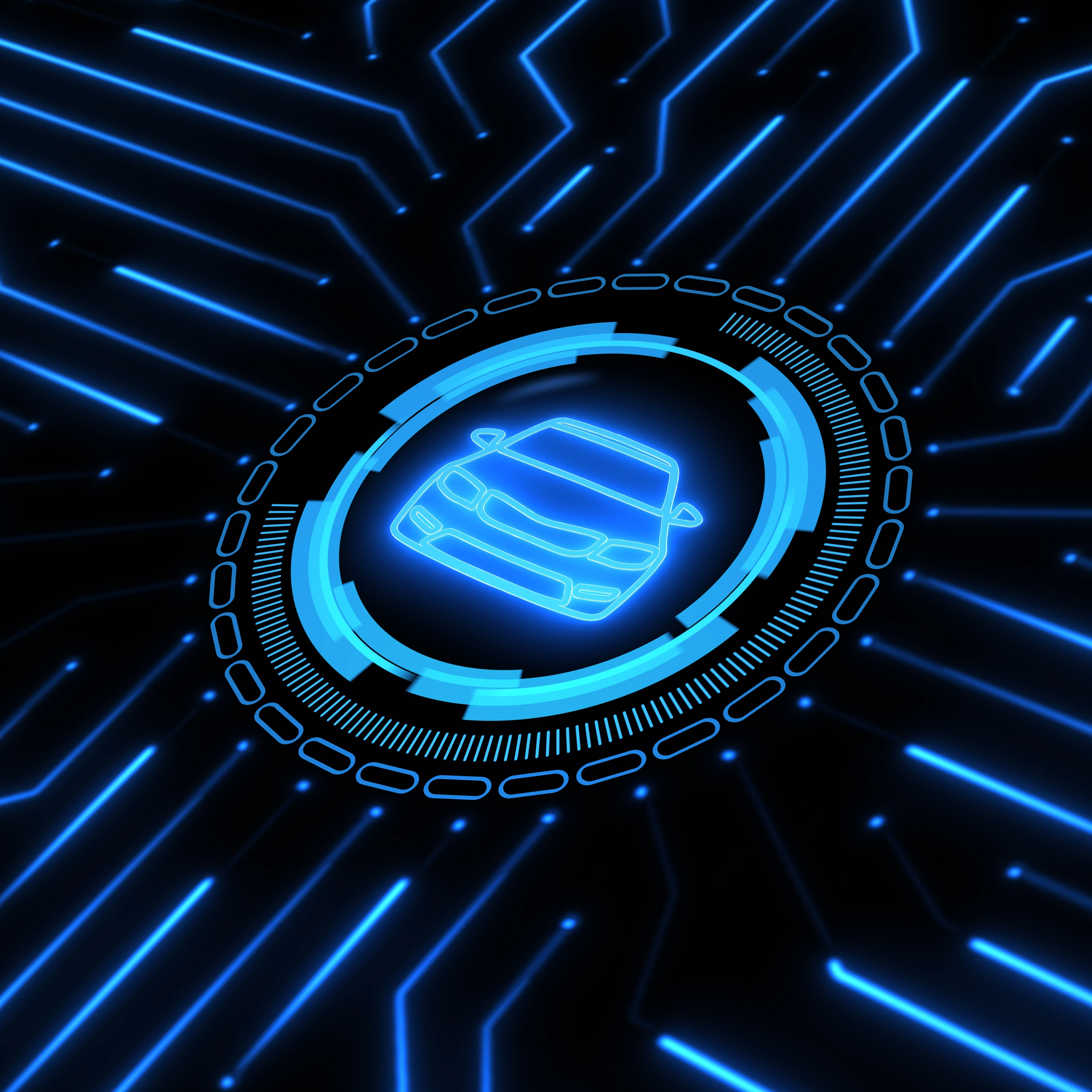
The CxO Summit at SEMICON Europa 2025 spotlighted Europe’s ongoing efforts to build a resilient and globally competitive semiconductor industry, while calling for greater ambition, speed, and unity in execution. Following global disruptions with the automotive supply chain crisis, the European Union launched a continent-wide strategy through the EU Chips Act. While the Act has already spurred significant developments, including construction of the new ESMC fab in Dresden, Europe remains far from its goal of achieving a 20% share of global semiconductor production by 2030. The CxO Summit, part of the SEMICON Europa event in Munich, provided an opportunity for industry leaders to share ideas about how to catalyze the next phase of the European industry’s growth.Ajit Manocha, President and CEO of SEMI opened the summit by describing today’s industry landscape with one word: “unprecedented.” Manocha said, “The global growth of the industry is unprecedented, with 107 new fabs set to come online by 2028, but the uncertainties are unprecedented, from geopolitics to the talent shortage to environmental concerns. So we need unprecedented solutions.” Ajit Manocha, President and CEO, SEMILaith Altimime, President of SEMI Europe echoed the mood of uncertainty, describing Europe as caught “in a perfect storm.” Altimime said, “As we face a combination of internal challenges and intensifying external competition, collaboration is not optional — it is mission critical.” Laith Altimime, President, SEMI EuropePierre Chastenet, Head of the Unit for Microelectronics and Photonics, European Commission, highlighted the tangible progress made under the EU Chips Act. “We now have a proper toolbox to handle a future crisis in the supply chain. The Chips for Europe initiative has led to the creation of five pilot lines for advanced technologies such as FD-SOI and wide bandgap semiconductors.” Chastenet added, “Europe must now capitalize on its strengths, from materials and equipment to design tools and cutting-edge research emerging from our RTOs.”Pierre Chastanet, Head of the Unit for Microelectronics and Photonics, European CommissionEchoing the call for action, Oliver Schenk, Member of the European Parliament, urged stronger regional unity. “Europe must act together, act faster, and act with much bigger ambition,” Schenk said, reinforcing the need for cross-border commitment to strengthen the continent’s semiconductor position.Oliver Schenk, Member of the European Parliament, European ParliamentHighlighting Europe’s most critical technology gap, Luc Van den hove, President and CEO of imec, unveiled plans for a new advanced fab backed by €2.5 billion in investment from the EU, the Flemish government, and ASML. Van den hove urged Europe to commit wholeheartedly to advanced technologies: “We must be more ambitious, and focus on disruptive breakthroughs rather than incremental change if we want to ensure a prosperous future.”Luc Van den hove, President CEO, imecAt the CxO Summit, CEA-Leti and ASML signed a memorandum of understanding (MoU) to deepen their collaboration and accelerate innovation in mainstream semiconductor technologies. Building on promising results in hybrid bonding, the partnership will now target 'More-than-Moore' innovations, including heterogeneous integration and novel substrates like SiC and GaN. “We aim to combine ASML’s world-class lithography expertise with CEA-Leti’s system-level innovation,” said Sébastien Dauvé, CEO of CEA-Leti. The collaboration is set to strengthen Europe’s ecosystem by shortening the path from early research to industrial impact.Left: Anne Hidma, Senior Vice President EUR US, ASML; Right: Sébastien Dauvé, CEO, CEA-LetiTurning to Europe’s industrial base, Christian Senger, CEO of Volkswagen Autonomous Mobility, emphasized the need to shift from risk-aversion to opportunity. While the region’s automotive sector faces intense global competition, particularly from China, Senger highlighted that Europe has the potential to lead in new mobility markets. “The market for autonomous roboshuttles for people transport in large cities is forecast to be worth €400 billion in the US and Europe alone,” he said. With American firms like Waymo and Uber leading the robotaxi space, Senger stressed that Europe must “act swiftly to create an environment that supports an autonomous mobility industry here.”Christian Senger, Member of the Board for Fully Autonomous Mobility and Transport CEO of ADMT GmbH, VolkswagenEurope’s Potential to Create Advanced TechnologyOne of these RTOs, CEA-Leti, is responsible for the FAMES pilot line for FD-SOI technology. Sébastien Dauvé, CEO of CEA-Leti, agreed with Pierre Chastenet that the pilot lines show great promise. He said, “FD-SOI is a big trend in semiconductors, because it enables very low power consumption in embedded devices. We think that adoption of the technology will grow in the coming years, and that is good, because most of the technology is produced in Europe.”Sébastien Dauvé, CEO, CEA-LetiEurope is also widely recognized to be the leading global voice on sustainability – a huge issue of concern to the semiconductor industry. Henri Berthe, President of the Semiconductor and Battery Segment at Scheider Electric, told the summit that 500 million tonnes of CO2 emissions per year are attributable to the semiconductor industry – “more than the whole of Mexico emits!” he said. “We need to make fabs more efficient, and that is why Schneider Electric has launched a new playbook with Applied Materials for sustainable energy abundance for the industry.”Henri Berthe, President of the Semiconductor Segment, Schneider ElectricAnother aspect of Europe’s playbook is support for new fabs. The flagship is ESMC, the joint venture between TSMC, NXP Semiconductors, Bosch, and Infineon. Christian Koitzsch, president and managing director of ESMC, reported to the summit that the project to build in Dresden a 12nm FinFET foundry and a 28nm CMOS line, requiring a total investment of €10bn, is on schedule. “We are now developing local supply chains, hosting a series of ESMC Supplier Days which are open not only to German but generally to European suppliers,” said Koitzsch.Christian Koitzsch, President and Managing Director, European Semiconductor Manufacturing Company (ESMC)As Manfred Horstmann, General Manager and Senior Vice President of Global Foundries, pointed out, the building of the ESMC fab means that Dresden is established as the center of a cluster of semiconductor industry companies. “Global Foundries has its Fab 1 and a mask center in Dresden. In fact, one-third of the chips produced throughout the whole of Europe now comes from Dresden.”Manfred Horstmann, General Manager and Senior Vice President, GlobalFoundriesAn example of ambition was given by Terence Gan, Executive Director of the Institute of Microelectronics of Singapore. Gan told the summit how Singapore has used pilot lines to stimulate research and development in new technologies. He said: “We started research into advanced packaging as long ago as 2011. Most people thought we were mad! But today, there is strong demand for our advanced packaging capabilities because of the rise of AI and its need for high-performance computing.”Terence Gan, Executive Director, Institute of MicroelectronicsBreaking Barriers to ProgressDespite momentum, bureaucratic inefficiencies continue to hamper progress. Narjiss Haddaoui, Managing Director of European Economics called for faster decision-making: “In global competition, speed is a decisive factor. To act fast enough, the EU must change its ‘software’ - the processes by which it considers and makes decisions.” Narjiss Haddaoui, Managing Director, European economicsThe stifling character of European bureaucracy is reflected in the region’s approach to building fabs. Herbert Blaschitz, Executive Vice President of Advanced Technology Facilities at Exyte, compared fab construction timelines: 20 months in Taiwan, 34 in Europe, and 38 in the U.S., attributing delays in Europe to paperwork bottlenecks.Herbert Blaschitz, Executive VP of Advanced Technology Facilities, ExyteFabio Gualandris, President for Quality, Manufacturing and Technology at STMicroelectronics raised another concern — 100% of raw materials used in European fabs come from outside the region. Christophe Frey, Vice-President for EU Engagements at Arm France, added that geopolitical tensions are clouding the path forward: “We are a bit lost in the smoke from the big fire in the world’s semiconductor industry.” Fabio Gualandris, President Quality, Manufacturing Technology, STMicroelectronics Christophe Frey, Vice-President of EU Engagements, Arm FrancePlaybooks For Future SuccessSo amid the uncertainty and global tension, what lessons can the industry learn from successful regional examples? Tuomas Korpela, Business Development Senior Manager at Nokia, credited Finland’s strategic procurement and policy tools with enabling a vibrant semiconductor ecosystem: “Finland creates demand for advanced chips using industrial policy tools, alongside strategic procurement in sectors such as defense and aerospace, and connectivity.” Tuomas Korpela, Business Development Senior Manager - Corporate Development Organization, NokiaAt a regional level, Joerg Schulze, Director of the Bavarian Chips Alliance, said that his organization was supported by the Bavarian State Ministry of Economic Affairs, as well as by companies and universities. “We help semiconductor companies to establish themselves and grow here through help with site searches, networking and contacts, funding and support, and talent acquisition,” said Schulze.Joerg Schulze, Spokesperson for the Bavarian Chips Alliance, Director of the Fraunhofer IISB, Bayern Innovativ GmbHCompanies in the European semiconductor supply chain also provided the summit with their insights into the roots of global success. André Grede, Chief Technology Officer of Comet, described how his company’s strategy is not to wait for customers to tell it what they need, but to be “ahead of the curve.” Grede said: “Is staying in sync with the customer enough? Not for us - we are deeply embedded with our customers, and constantly looking to broaden our relevance to them.”André Grede, CTO, CometChristophe Maleville, Chief Technology Officer of Soitec, provided a real-world example of how this is done. He said: “Our engineered substrates using RF-SOI technology reduce the drain on a mobile phone’s battery power, and cut our customers’ board footprint thanks to RF front end integration. As a result, our products are now in 100% of 5G smartphones.”Christophe Maleville, CTO, SoitecAnne Hidma, Senior Vice-President for Europe and the US at ASML, shared the company’s success formula: “The reasons for ASML’s success include customer focus – decide which markets you are going to be in, and which you are not. We are also all-in on innovation. We nurture an ecosystem, which for us includes imec and CEA-Leti, as well as partnerships with academia. And lastly, we have a strong supply base, which is a core strength of Europe.” In a time marked by both uncertainty and opportunity, the example of ASML shows how the European semiconductor supply chain can survive and thrive.Anne Hidma, Senior Vice President EUR US, ASMLEurope’s Path ForwardThe CxO Summit made one thing clear: Europe has world-class innovation, policy momentum, and industrial commitment. What’s needed now is faster execution, deeper collaboration, and the courage to invest in the technologies of tomorrow. As the industry heads toward the $1 trillion milestone, the decisions made today will shape Europe’s place in the semiconductor world for decades to come.On behalf of SEMI, the SEMI Europe team would like to express appreciation to the industry leaders for sharing their visions and readiness to collaborate during the CxO Summit.SEMI ContactLaith Altimime, President SEMI [email protected]
Read More
Q3 2025 was packed with activity. From finalizing the Standards program for SEMICON West, to organizing the event’s corresponding Global Standards Summit (GSS), the Standards team is excited to share its most recent quarterly developments.On Tuesday, October 7, leaders from across the industry convened in Phoenix, Arizona, for the second annual GSS. This half-day summit focused on future standardization needs for supply chain traceability and environmental sustainability. In addition, the Standards team conducted two workshops at SEMICON West. The first, SEMI Liquid Chemicals Analytical Workshop, detailed recent advances in analytical methodology and instrumentation related to particle measurement, trace metals, and organics in liquid chemicals. The second, Enhancing Voltage Sag Immunity: SEMI F47 Standards Updates Insights Workshop, offered a forum for sharing improvements to SEMI Standard F47 to further enhance tool performance and reliability. Finally, Q3 saw the official introduction of SEMI Standards T26 and E195. SEMI T26-0925, Specification for Electronic Supply Chain Traceability Using Distributed Ledger Technology, will be crucial for improving security and transparency for the industry’s supply chain. Additionally, SEMI E195-0925 is now available for purchase. This standard, Test Method Using Adhesive Replacement Substrates to Assess Particulate Surface Contamination on Critical Chamber Components, offers a testing approach for measuring the ISO 14644-9 cleanliness of a critical chamber component.To participate in upcoming standard developments, learn more about becoming a member of the SEMI International Standards Program. Global Standards Summit The SEMI GSS made its North American debut at this year’s SEMICON West in Phoenix. Building on its inaugural event at SEMICON Japan 2024, GSS is a strategic forum dedicated to creating an industry-wide standardization roadmap for the next three and seven-year benchmarks. The 2025 GSS continued conversations from SEMICON Japan on environmental sustainability, while expanding its program to include supply chain traceability. As geopolitical tensions, mounting cybersecurity threats, and rising technological demands continue testing the limits of the industry’s supply chain, the need for global standardization is becoming increasingly apparent. The 2025 GSS program addressed these concerns and others across multiple sessions, offering insight on how these challenges are being addressed in the industry while highlighting critical areas still in need for standards development. Key outcomes from the GSS program include: Addressing data sharing across multiple supply chain tiers while protecting IP rights and a call for harmonization across standards. The presentation by Randy Hall from the Provenance Chain Network, offered approaches on how data owners can share information with authorized users without compromising sensitive manufacturing details. While there are standards gaps that hinder broader adoption, there is opportunity to address insufficient visibility across the industry’s supply chain amid ongoing cybersecurity threats by harmonizing across existing standards implementations. An integrated modeling framework for informing energy efficiency and carbon reduction approaches. Developed by the International Roadmap for Devices and Systems (IRDS) Environmental Sustainability for Semiconductor Facilities (ESSF) team, this effort helps address demands for maintaining rapid technological progress while still meeting the industry’s ambitious sustainability goals.Standardization opportunities for improving sustainability within manufacturing facilities. Nate Monosoff from Jacobs offered insight into the decision-making tradeoffs that balance sustainability with other facility performance areas, focusing on standard methods for calculating ESG performance. GSS concluded with a panel discussion that featured leaders from AMD, FTD Solutions, Intel, The Provenance Chain Network, Jacobs, Qualcomm, and Tokyo Electron. In this session, our thought leaders discussed the fundamental importance of standardization for our industry, standards adoption, incentivizing stakeholders, and how standards can be designed to remain flexible and adaptive as technologies and regulatory landscapes evolve. SEMI Standard T26In line with the 2025 GSS theme of supply chain traceability, the Standards team is pleased to introduce SEMI T26, Specification for Electronic Supply Chain Traceability Using Distributed Ledger Technology. This standard was published in September to define a secure and decentralized traceability system that all members of the electronics supply chain can safely share. This system is based on distributed ledger technology to improve industry-wide reliability assurance.Update on Document 7130CIn February, Document 7130C was approved during the North America Metrics Technical Committee Chapter Meeting. The document officially became SEMI E195 - Test Method Using Adhesive Replacement Substrates to Assess Particulate Surface Contamination of Critical Chamber Components in September.SEMI E195 describes a quantitative method for measuring the ISO 14644-9 surface cleanliness for particle concentration of a critical chamber component (CCC), by means of an adhesive replacement substrate. The purpose of this standard is to ensure measuring and reporting consistency across CCCs or processing equipment manufacturers. To help acquaint the industry with this standard, SEMI offered a combined, in-person course on SEMI E194 and SEMI E195 during SEMICON West. The course provided fundamental information on each standard, in addition to other process approaches for improving reliability and yield.Other SEMI Updates:SEMI Preventive Maintenance Automation White Paper SEMI Korea conducted a Global PM Automation Survey in August to better understand today’s preventive maintenance readiness issues for autonomous fabs. The results will be included in SEMI’s upcoming PM Automation Whitepaper and will ultimately guide future developments for related SEMI Standards. Standardized Semiconductor Cyber Assessment FrameworkIn Q3, the Semiconductor Manufacturing Cybersecurity Consortium (SMCC) released its Standardized Semiconductor Cyber Assessment (SSCA) framework. This document provides a detailed cybersecurity readiness plan for semiconductor companies across the supply chain. Its goals are to standardize industry-wide cybersecurity risk evaluations, establish and accelerate the adoption of best practices, and improve information sharing and collaboration. Download the SSCA framework for free.New Data Standard for Equipment Edge Governance In June, Document 6938C was approved during the Taiwan Information Control Technical Committee Chapter Meeting. The document officially became SEMI E196 - Guide for Equipment Edge Data Governance. SEMI E196 provides guidance for identifying equipment data supplied by manufacturers that can be used in equipment engineering or analysis applications.New Guide to Meet IRDS Yield Table RecommendationsAt the NA Summer Meetings, Document 6601B passed TC Chapter review with technical changes and a Ratification Ballot was issued in Cycle 7-2025. Pending final Procedural Review, Guide for Meeting IRDS Yield Table Recommendations for High Purity Polymer Materials and Components Used in Ultrapure Water, will cover areas that establish criteria for allowable contribution by critical components used for UPW treatment plant and distribution system. This document will be proactively updated to manage the risks associated with the high purity polymer materials used in the semiconductor process. The biggest challenges today are metals and particles and certain organics.Flex Standards Meeting at FLEX 2026Meet the leaders of the SEMI Standards Flexible Hybrid Electronics (FHE) Task Forces at Flex 2026, in Arizona, February 24-26, and learn about ongoing FHE standardization efforts!Standards Introduced in Q3 2025New and revised standards released in Q3. July 2025 StandardsAugust 2025 StandardsSeptember 2025 Standards Get InvolvedSEMI Standards development activities take place throughout the year in all major manufacturing regions. To participate, join the SEMI International Standards Program.SEMI Standards are available through individual download purchases or online via SEMIViews. Sign up for a 30-day SEMIViews trial.For more information, please visit the Standards website and events page. For any questions regarding SEMI Standards activities, please contact your local SEMI Standards staff. Paul Trio is Director of Standards at SEMI.
Read More
As the global economy increasingly prioritizes sustainability and climate action, corporate renewable energy procurement has emerged as a critical tool worldwide. To achieve their corporate sustainability goals, businesses have sought to secure renewable energy through Corporate Power Purchase Agreements (CPPA) with renewable energy developers. Overview of System Charges: Their Role and Impact on Corporate Renewable Energy ProcurementCPPAs are one of the common approaches for businesses to procure renewable energy directly from renewable energy developers. Physical CPPAs involve two major cost components – energy costs and system charges. In this blog, we focus on system charges which are fees collected by utilities that include transmission and balancing components. Transmission charges cover the use of grid infrastructure to deliver electricity, while balancing charges cover the cost of maintaining real-time supply-demand stability.Although system charges are a key cost component in physical CPPAs, they are typically not the primary cost drivers. Based on Wood Mackenzie’s cost estimate analysis for a 50-100MW solar CPPA across the various regulated and liberalized APAC markets of Malaysia, Thailand, Australia, Philippines, South Korea, Singapore, Japan and Taiwan, system charges typically make up less than 20% of the total CPPA price. However, this share of system charges in the total CPPA price varies considerably between APAC markets. Australia, the Philippines and South Korea maintain system charges at between 10% - 20% of their solar CPPA prices. Singapore, Japan and Taiwan see the lowest proportion of system charges of solar CPPA prices at 7%, 6% and 5% respectively.Malaysia's Moment: Optimizing SAC for CRESS SuccessAnnounced in July 2024, CRESS allows for physical CPPAs from renewable energy projects of 30 MW and above. While CRESS opens new avenues for businesses to access renewable energy, the implementation of the System Access Charge (SAC), a surcharge imposed on renewable developers for using the Malaysian Grid under CRESS, has raised cost concerns within the industry.Based on Wood Mackenzie’s analysis, Malaysia's SAC account for about 60% of the estimated total CPPA price in Peninsular Malaysia, assuming a solar production cost at USD57/MWh (based on the average of the large scale solar LLS3 LLS4 - bid price range of MYR 0.19-0.28/MWh. The SAC significantly impacts the overall cost structure of renewable energy procurement. Malaysia’s SAC for solar “non-firm supply” under CRESS is currently set at 40sen/kWh or about USD/MWh making them the highest system charges applicable to CPPAs in the region.Another concern relates to cost-transparency and ease of long-term cost forecast for buyers. Most APAC markets demonstrate high transparency in their methodologies for determining system charges. Countries like Australia and Japan provide clear breakdowns of cost components, including grid capital expenditure, operation expenditure, power losses, ancillary services, and market operation costs. Even after analyzing other regulated markets like Thailand (where wheeling and balancing charges are based on UGT 2 tariff rates), Taiwan and South Korea, Malaysia’s SAC lacks transparency in its the system charges determination methodology, compared to three other vertically integrated Single Buyer markets like Peninsular Malaysia. Such cost transparency, including detailed cost components and calculation methodology, is crucial for corporate energy buyers looking to increase predictability of electricity costs by entering long-term CPPAs. The high SAC charge poses a significant barrier to the adoption of renewable energy by industrial end-users like semiconductor manufacturers and makes it challenging for prospective CRESS buyers to understand how these charges may evolve over a 21-year contract period. The SAC under CRESS would be reviewed every 3 years and is subjected to a maximum variation of 15% from the prevailing charge.RecommendationsThe lack of transparency of the SAC could jeopardize Malaysia’s critical development objectives, such as attracting MYR500 billion (USD $110 billion) in semiconductor investments by 2030 under its National Semiconductor Strategy (NSS), or its 40% renewable installed capacity target by 2035 (or about 18 GW by 2035). To address these challenges and create a more favourable environment for both semiconductor investments and renewable energy adoption, SEMI and Wood Mackenzie propose the following recommendations:Benchmarking SAC against transparent and established system charge components: Additional transparency would allow Malaysia to align with practices in both regulated and liberalized markets across the APAC region and allow more players to make long-term investments in Malaysia. Similar cost methodologies to the regulated tariff could be adopted. As an initial step, SAC should reflect Network Charges defined under the regulated tariff, and as a best practice, any differences between the SAC and the Network Charges in the regulated tariff should be clearly explained and justified (e.g. additional balancing costs induced by solar procured under the CRESS may be audited with the Single Buyer).Improving CRESS SAC stability and predictability: Ensuring transparency on the calculation methods behind SAC and its components, and predictable SAC levels, will allow businesses to proactively anticipate and plan for renewable energy procurement expenses, enabling informed decisions and on long-term corporate solar PPAs spanning 20 years’ time horizon under the CRESS framework. In particular, the maximum change in SAC charges can be narrowed down from 15% every three years.4Alignment of national sustainable energy policies: Strengthening policy support and ensuring accessible financing are essential to driving the widespread adoption of renewable energy. CRESS can only succeed if the scheme enables fair, transparent, and competitive access to clean energy. New renewable energy coming online via CRESS should not be put at an economic disadvantage through differentiated system charges from those applicable to other clean energy schemes. For example, no SACs are applied to solar under Large Scale Solar (LSS) projects, despite their system impacts being the same as under CRESS. Sustained efforts to improve affordability within CRESS are crucial for attracting investment, reducing the cost of SAC for buyers, and accelerating Malaysia’s transition to a sustainable, low-carbon future.The Path Forward and ConclusionImproving transparency and stability of SAC is crucial for facilitating Malaysia's development goals in semiconductor investments and renewable energy targets. By implementing these recommendations, Malaysia can enhance its competitiveness in attracting sustainable investments and accelerate its transition to clean energy.As the voice of the global electronics manufacturing and design supply chain, SEMI is committed to working with policymakers, industry leaders, and stakeholders to address these challenges. SEMI and Wood Mackenzie believe that by fostering a more transparent and competitive environment for renewable energy procurement, Malaysia can unlock the full potential of the country’s semiconductor industry while contributing to a more sustainable future.SoYoung Jang manages the SEMI Energy Collaborative programs at SEMI.Antoine Gaudin and Chun Kang Eu are from Wood Mackenzie.
Read More
SEMICON West in Phoenix, Arizona, will bring together all of the SEMI Sustainability efforts and programs under one roof over three days. With back-to-back sessions from October 7-9, this year’s Sustainability EHS Program will offer expert insights on the most pressing sustainability topics facing the microelectronics industry. Tuesday will kick off the program and focus on the business aspects of driving to sustainability in the semiconductor sector. On Wednesday, the Pavilion hosts discussions on water risk, water management, circular economy solutions and the needs for innovation from startups. Finally, Thursday will highlight the current emissions landscape, milestones and achievements, and solutions developed by the SEMI Semiconductor Climate Consortium (SCC). The 2025 event also marks the first public discussions of the full scope, findings and status of the SCC’s direction.All three days of the Sustainability EHS Program are sponsored by Edwards, Schneider Electric, TEL, SCREEN, Sundt and the Greater Sacramento Economic Council. Here’s a sneak peek at what the 2025 program has to offer. Registration for SEMICON West is open.The Business of Sustainability – Tuesday, October 7 Sustainability Panel: Path to Success Sustainability hits the keynote stage with Tuesday afternoon with a panel discussion detailing a plan for meaningful sustainability progress. The panel, titled Sustainability Panel: Path to Success—The Semiconductor Industry Leads the Way for a Resilient Future, will take place on the CEO Summit Keynote Stage from 2:35-3:35 p.m. Experts from Applied Materials, BASF, Micron, Google, and Qualcomm will cover strategies on how collaboration, supplier engagement, and clean technology investments are reducing emissions and propelling the industry closer to its sustainability goals. Attendees will discover what’s working, what’s still to come, and how the industry will forge its way toward a more sustainable future.A Musical Performance by Ay YoungIn anticipation of the Path to Success panel discussion, Tuesday will also spotlight an exciting musical guest. AY Young is a singer, songwriter, and the founder of the longest-running clean energy concert series in the U.S. At 2:20 p.m., he’ll take to the CEO Summit Keynote Stage for a memorable performance and give a glimpse into how important sustainability has become to attract a new generation of talent. Through his musical talent and deep commitment to clean energy, Young was appointed as a United Nations (UN) Young World Leader in 2020, helping the organization further its 17 Sustainable Development Goals. His Project17 initiative is a 17-song album, with each song centering on a different goal and backed by a corporate sponsor that aligns with it. Young will also attend the Sustainability Reception from 5-6:30 p.m. at the Sustainability Pavilion Theater.EHS Regulatory OverviewThe wide range of regulatory topics will be showcased in the first session on Tuesday at the Sustainability Pavilion. Expert speakers and advocacy groups will deliver key insights on the threats and challenges, and the research and collaboration opportunities currently at play in the regulatory environment, with special focus on keeping electronics manufacturing strong. Climate Equity Social Impact Workgroup (CESI) Aligning with the theme of the UN Sustainable Development Goals, the SEMI Climate Equity Social Impact (CESI) Working Group will highlight how its members are progressing real-world outcomes for climate, education, and global cooperation. This session will run from 3-4 p.m. at the Sustainability Pavilion Stage, and it’s ideal for anyone in the industry who’s passionate about sustainable partnerships. Innovations Enabling Reduce, Reuse, Repurpose and Recover – Wednesday, October 8Resource Use and Circular EconomyWednesday’s 10:15-11:30 a.m. session, Resource Use and Circular Economy will offer tactical solutions to help fabs reach up to 80-90% circularity. The goal of this session is to lay a foundation for transforming the industry’s circularity concerns into practical opportunities, which will be achieved over two panel discussions. Discussion 1, A Circular Value Chain: Challenges and Leading-Edge Solutions, will highlight solutions for eliminating waste and reducing manufacturing costs through circular technologies. This panel will feature experts from Edwards, Syensqo, and ElectraMet and will be moderated by Subgeni’s Taimur Burki. These subject matter experts will highlight their company solutions, but also other areas they see in need of consideration from a circularity lens, as well as best known practices across fabs. Water is a precious resource, and how the industry manages it is crucial for its long-term success. Discussion 2, Tactical Maturity Scales for Water Management, will unveil two new guides developed by SEMI’s Water Management Working Group. Both products are designed to move manufacturers from both large and small fabs and manufacturing operations to assess their water needs and most efficiently improve water reuse by up to 80%. This panel will be led by speakers from Aquatech, SCREEN, Sundt, Ovivo, and C2MI. Water Resilience Starting at 11:30 a.m. at the Sustainability Pavilion Stage, attendees will hear from the SEMI Environmental Risk Mitigation and Reporting Working Group lead - Senior Sustainable Program Manager – Alua Suleimenova – as she shares her insights and findings from a recently completed study by WaterPlan on industry water risks within the semiconductor value chain. The topic and findings will then be addressed by a panel, where Suleimenova will engage leaders from ASM, Waterplan, ERM, and the Alliance for Water Stewardship, in a conversation about water, nature, and associated corporate risks. Although companies are making strides to protect water access, it’s becoming clear that a focus on internal activities will not move the needle significantly enough for achieving long-term resilience. This panel will offer solutions for adapting water-related risks to the supply chain, with a focus on North America, Asia Pacific, and Europe.Other Wednesday AttractionsSEMI S3 – Startups for Sustainable Semiconductors: SEMI S3, or Startups for Sustainable Semiconductors, is an annual program by the industry’s venture capital divisions designed to boost awareness of semiconductor industry needs by inviting promising startups to be mentored and pitch their solutions to our industry. Earlier this year, 145 candidates submitted applications. Now, it’s down to 15 finalists, who will present at SEMICON West from 2-4:40 p.m. at the Sustainability Pavilion, following a Fireside Chat from experienced innovation experts from 1-2pm.Accelerating Sustainability with Smart Manufacturing – Presentations Poster Session: Technical papers and posters focused on sustainability solutions – from water to energy – will also be presented in the Smart Manufacturing Pavilion from 2-5:15 p.m., providing an opportunity to network with industry leaders and discover the latest best practices for how machine learning and AI can reduce water and waste in fabs.Reducing Emissions – Thursday, October 9SCC – Tackling Emissions Across the IndustryExpect a full-house at Thursday’s all-day session featuring SCC – Tackling Emissions Across the Industry. From 10:15 a.m. to 3:00 p.m., the SEMI SCC leaders and experts will detail its findings and projects addressing the industry’s emissions. SCC has been focusing on ensuring consistent and measurable progress in decarbonizing from 2021 levels. Key topics include: Reporting and aligningBaseline, ambition, and roadmapAbatementLow Global Warming Potential (GWP) gases workLow Carbon Economy (LCE) access and procurementEnergy efficienciesScope 3 upstreamSEMICON West also features SEMI U courses to learn more about sustainability in our industry. For example, on Thursday, SEMI U: PFAS Compounds in Semiconductor Environment, is being offered from 8 a.m. to noon. This course is available for purchase. Support the SEMI Forest community effort to reforest our planet by funding a range of certified carbon avoidance and tree planting projects. Our goal for SEMICON West is to fund planting for 100,000 trees. Scan the QR code below to contribute and help us meet our goal.Learn more about the 2025 SEMICON West Sustainability EHS Program. Follow SEMI Sustainability on LinkedIn for regular updates on sustainability initiatives. Saifi Usmani is Vice President for Sustainability at SEMI.
Read More
AI is proliferating rapidly, fueled by ever-larger models and data sets that are expanding AI use cases and improving its accuracy. Future computing systems are now required to simultaneously deliver high performance, process large amounts of data, and use the least possible energy. The growing energy footprint of AI and the strain it places on the power grid is an increasing concern for companies and even entire countries. This could adversely impact future growth and could slow the semiconductor industry’s march towards $1 trillion in revenue, which is largely driven by AI applications.This is a formidable challenge that cannot be addressed in silos by individual companies or even industry segments. The SEMI Smart Data-AI Initiative is exploring how to overcome this challenge with collaborative and innovative system-level solutions that connect the dots across the entire AI system stack. In March 2025, we hosted a successful workshop, bringing together industry leaders across the value chain for a day of thoughtful discussions and knowledge sharing. Building on this foundation, we developed an exciting Smart Data-AI session to be held at SEMICON West in Phoenix, Arizona on October 7 from 10:30 a.m.-4:40 p.m. The “Future of Computing: Energy-Efficient Computing for AI and Beyond” forum will bring together executives and thought leaders across the entire ecosystem – including design, fabrication, interconnects, system integration, hyperscale architectures, advanced materials, and emerging technologies such as photonics and quantum. Attendees will have a unique opportunity to get strategic perspectives from these distinguished experts and learn about exciting future trends.Why Attend?Gain insights from global leaders and learn about innovative paths towards an energy-efficient computing future.Network and build cross-industry collaborations for the next wave of AI, photonics and quantum.Promote a more sustainable path for continued growth of AI to benefit humanity and the planet.Join the SEMI Smart Data-AI initiative to develop solutions and take concrete actions to reduce AI’s growing energy footprint.Support the industry in achieving its goal of reaching $1 trillion in revenue. Speaker Highlights Include:AMD • Ciena • Hewlett Packard Enterprise • IBM • Merck KGaA, Darmstadt, Germany •Microsoft • Quantum Economic Development Consortium • Rapidus • Rigetti •Siemens AG • Stanford UniversityDr. Pushkar P. Apte is the Strategic Technology Advisor and leads the Smart Data-AI Initiative at SEMI.
Read More
As the volume of regulations grows across all levels of government, both in the U.S. and abroad, the semiconductor industry is increasingly struggling to keep up with its reporting obligations. Potential consequences include shipments delayed by customs, existing stocks of materials, parts, and components unexpectedly being made obsolete, and disruptions to multiple tiers of the supply chain that persist over time.To minimize the burden of numerous, varied reporting expectations, the SEMI PFAS Transparency Working Group, led by Intel and Tokyo Electron, is working to:Enable standardized communication on the presence of Per- and polyfluoroalkyl substances (PFAS) in chemical formulations, materials, tools, parts, and fab infrastructure to minimize the burden of varied reporting expectations;Enable traceability; andProtect confidential business information. While the initial focus of the effort is on PFAS, the intent of the group is for the methodology to be applicable to other substance reporting requirements.The group will be holding a working session at SEMICON West in Phoenix, Arizona on Wednesday, October 8 from 10:30 a.m.-12:00 noon at the North Building, 200 Level, Room 229A of the Phoenix Convention Center. All segments of the semiconductor manufacturing supply chain are invited to join the meeting and contribute to this critical effort. This session is intended for individuals involved in: Data management and reportingSupply chain managementMajor business continuity planning and crisis managementRisk assessment and mitigationEHS/regulatory complianceSub-supply chain visibility challengesThe PFAS transparency effort will also be introduced during the SEMI EHS Summit and SEMI Global Standards Summit, both scheduled on Tuesday, October 7.For additional resources, download the PFAS Explainer or SEMI PFAS Position Paper. Contact [email protected] for questions or more information about the working group session.James Amano is Senior Director of EHS at SEMI.
Read More