downloadGroupGroupnoun_press release_995423_000000 copyGroupnoun_Feed_96767_000000Group 19noun_pictures_1817522_000000Member company iconResource item iconStore item iconGroup 19Group 19noun_Photo_2085192_000000 Copynoun_presentation_2096081_000000Group 19Group Copy 7noun_webinar_692730_000000Path
Skip to main content
Default Banner Image

United States

Yesterday, President Trump extended the deadline for List 3, which would have raised U.S. tariffs on $200 billion worth of goods from China. SEMI welcomes the deadline extension.Over the past three months, the United States and China have engaged in bilateral discussions to address structural issues like intellectual property protection and requirements for the use of joint ventures as well as trade balance concerns. President Trump announced that these talks have yielded significant and substantial progress in all areas. That said, it’s been reported that discussions on structural issues, such as forced technology transfer, have seen limited progress.Certainly, questions remain on the specifics of liberalization, the structure of the agreement and, most notably, enforcement. Any new commitment will be toothless without a firm and binding enforcement mechanism. While the date of the new deadline hasn’t been clarified, we believe that the tariffs won’t be increased before Presidents Trump and Xi meet, which could happen in late March at Mar-a-Lago.List 3 covers a range of items, including a number of consumer goods, but also directly impacts items critical to the semiconductor manufacturing process, including materials and machines. SEMI estimates that all U.S. and Chinese retaliatory tariffs – which hit machines and tools central to the semiconductor industry, including equipment used to manufacture wafers, boules, and chips as well as test, inspection and sensing equipment – will cost members more than $700 million in annual duties.While SEMI strongly supports stronger protections for valuable intellectual property (IP), tariffs will not help address Chinese trade practices and will ultimately have significant and unintended consequences. SEMI asserts that these tariffs will harm companies in the semiconductor supply chain by increasing business costs, introducing uncertainty, and stifling innovation. The tariffs seem to target U.S. firms for simply operating in China.Given that chips, tools, and materials are extremely complex, precise, and difficult to manufacture, it is not reasonable to believe that any component can easily be replaced with a part from another source. Further, this U.S. government approach does not take into account that many items subject to these tariffs are not available, at sufficient quality and cost, from domestic sources, or even non-Chinese sources. We stand steadfast in our belief that this trade action will raise prices, put thousands of high-paying and high skill jobs at risk, and curb growth.SEMI will continue monitoring new developments in this area. Any SEMI members with questions should contact Jay Chittooran, Global Public Policy Manager at SEMI, at [email protected].
Read More
The more than 53,000 people who flocked to SEMICON Korea last month were treated to a motherlode of insight into the future of the semiconductor industry as 470 companies exhibited innovative technologies in more than 2,000 booths. But the annual event’s most arresting numbers came in keynotes and other presentations pointing to the extraordinary industry growth that lies ahead.“It is no exaggeration to say that 90 percent of the world’s data has been generated in the last few years,” said Jim Feldhan, president of Semico Research. “This explosive growth of data is expected to continue. That's why server shipments will grow by 20.3 percent, or 30 million units, this year alone.”Feldhan said that the Internet of Things (IoT) will be a chief driver of semiconductor industry growth, with IoT expected to be applied in areas as varied as automotive, smart cities, edge computers, finance, architecture, agriculture and healthcare. For its part, artificial intelligence (AI) will start to exercise human-like judgment. Feldhan noted that in many instances in these fields, “it is more accurate to apply AI and vision systems than to rely on traditional decision-making.”Yoon Jong Lee, senior vice president of DB HiTek, predicted that the Internet, AI and 5G will drive market growth. “Looking back over the past 30 years, semiconductor market growth was powered by PCs, the Internet and cell phones, yet last year memory accounted for 35 percent of total semiconductor sales, more than double the figure in 2016,” he said. He predicted that, in 2019, the foundry sector will outstrip the semiconductor market in growth, noting that the average growth rate of the semiconductor industry is expected to be 4.1 percent, compared to 7.1 percent for the foundry market. Clark Tseng, director of SEMI, reported that the strong semiconductor growth in 2018 is unlikely to continue in 2019 due to the decline in memory pricing, as well as mobile and PC demand. “Demand for semiconductors is likely to decline in the first half as the industry is still digesting inventory and rebound in the second,” Tseng said. Semiconductor industry growth headwinds include decreases in high-end smartphone purchases, PC demand and demand for DRAMs for servers in data centers, Tseng said. Declines in economic growth and consumption in China and the U.S.-China trade war will also contribute to a slowdown. However, Tseng noted that, over the long term, technology innovation will continue and that the semiconductor industry’s prospects remain bright.One key innovation will be the elimination of AI’s reliance on Internet connections in the future. In his opening day keynote, Eunsoo Shim, senior vice president at Samsung Electronics, emphasized that AI technology that operates without the Internet in the future is essential. “We are developing 'on-device AI' technology that incorporates AI algorithms in products such as smartphones and autonomous vehicles,” he said. "When on-device AI technology is implemented, it reduces reliance on the Internet, battery consumption, and data latency.” Reducing latency will significantly improve device response time.Walden C. Rhines, CEO Emeritus of Mentor, a Siemens business, predicted that AI will fuel rapid memory growth. The memory semiconductor (DRAM, NAND flash) market is expected to see a temporary slowdown this year, with the market expected to rebound in 2020. Rhines said that memory could be seen as an early market with rapid future growth, citing memory market super-booms in 1995 and 2000.“Memory production has not decreased since 1995 or 2000,” he said. “Although memory prices will temporarily fall this year after significant market growth in 2017 to 2018, the market will continue to grow as memory production increases,” he said. Rhines added that “although memory prices will drop by about 10 percent this year, he believes prices will increase 6 percent next year.” He also predicted the steady growth of the non-memory semiconductor market as AI technology matures and China’s investment in fabless companies continues.Indeed, SEMICON Korea speakers made it clear that concerns about the growth of the semiconductor industry are expected to be short-lived. While overall growth is likely to slow in 2019, the industry is expected to rebound steadily – powered by the semiconductor industry paradigm shift led by AI, IOT, and autonomous driving – and reach a new high of nearly $541 billion in 2020.Jaegwan Shim is a marketing specialist at SEMI Korea.
Read More
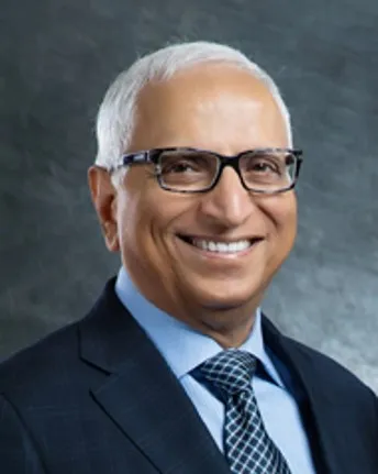
Last year the industry posted another remarkable double-digit revenue growth year. IC shipments eclipsed one trillion units for the first time and continued to enable an ever-expanding array of silicon intensive-applications.2018 was also a pivotal year of transformation at SEMI. Setting our sights firmly on building more value for SEMI members, we doubled down on priorities I established this time last year. We advocated intensively on global trade policies, industry talent needs, and critical environment, health and safety (EHS) concerns. To underpin our efforts around talent, we took the bold step to reinvigorate the industry’s identity with a dynamic image campaign. Above all, we targeted critical industry-wide issues to help us realize the ambition of becoming a trillion-dollar industry in the next decade. Workforce DevelopmentRedefining our approach to talent development in 2018 was and remains a top priority. A diverse, highly skilled workforce is crucial to the industry’s ability to innovate. Last year we ramped up a number of SEMI High Tech U (HTU) programs to inspire young people and attract them to careers in high-tech manufacturing. To date, more than 130,000 students have been touched by HTU – through student or teacher programs.Over the past year, we designed a new university outreach program and established partnerships with 100 institutions. We established Workforce Pavilions at SEMICON events in Southeast Asia, the U.S., Taiwan, Europe and Japan for students to explore career opportunities and meet with recruiters. We thrilled at seeing sponsors hire young talent at SEMI events. This year, all SEMICONs worldwide will feature Workforce Pavilions.SEMI also formalized its commitment to Diversity and Inclusion (D I) with the establishment of a D I council to shape new programs including the recently launched Spotlight on SEMI Women. To localize and fully optimize our D I programs, we established regional workforce councils in every region we serve. We unveiled the SEMI Mentoring Program to support students and young professionals on this journey by facilitating one-on-one mentoring relationships with industry professionals. Hundreds of mentees have enrolled. But we still need more mentors. I urge you to join the program. During the year, SEMI also expanded its workforce staff and developed a comprehensive workforce strategy with programs that engage students as early as elementary school and inspires them through high school and college. The program provides pathways to professional careers, building a pipeline to fill the short-term and long-term talent needs of the industry. Industry Image CampaignAs we developed the comprehensive workforce development program, we knew we had to refresh the industry’s image and appeal to the next generation through contemporary media and communications channels. So we recently launched a bold, innovative campaign to raise industry awareness and attract students and recent graduates to careers in semiconductor manufacturing.Our You’re Welcome campaign is a novel, creative approach that blends entertainment, media and storytelling to excite students about the industry. The campaign went viral immediately and within weeks had more than 5.5 million social media impressions and 2.3 million video views.Trade Policy AdvocacyRising trade tensions between the U.S. and China catapulted global trade policy to the forefront of industry concerns in 2018. Since the tariffs have taken force, semiconductor companies have faced higher costs, greater uncertainty, and difficulty selling products abroad. The tariffs have forced many SEMI member companies to pause or rethink their investment strategies.SEMI quickly engaged U.S. policymakers and provided resources for SEMI members. We formed a member trade task force, staged trade compliance seminars in China, and convened meetings with over 110 U.S. congressional, agency and administration officials, and provided testimony on the importance of the free trade to the industry.SEMI continues to educate policymakers about the critical importance of free and fair trade, open markets, and respect and enforcement of IP for all players in the global electronics manufacturing supply chain. As part of this initiative, we distributed “10 Principles for the Global Semiconductor Supply Chain in Modern Trade Agreements” and encouraged their adoption in various trade negotiations. These principles outline the primary considerations for balanced trade rules that benefit SEMI members around the world, strengthen innovation and perpetuate the societal benefits of affordable microelectronics.Environment, Health and SafetyEnvironmental regulations are proliferating globally even as advanced semiconductor manufacturing technology relies increasingly on a host of new materials. With dozens of new fabs and fab line upgrades, our industry must align on best practices, sensibly respond to materials restrictions, and renew efforts toward sustainable manufacturing.That’s why the revitalization of SEMI EHS efforts became another priority in 2018. Two months ago, we hosted the inaugural EHS Summit at SEMI Headquarters. Fully, 70 EHS professionals and company executives met to form the basis for the future SEMI EHS program.The Year AheadDespite a softening in the market, compounded by Apple’s first-ever announcement of a revenue decline in 16 years, a geopolitical whirlwind on trade and an extended shutdown of much of the U.S. government, the future is bright.At SEMI’s annual Industry Strategy Symposium (ISS 2019) in Half Moon Bay, Calif. in early January, the sense of optimism was palpable. In her keynote address, Dr. Ann Kelleher, Sr. VP and General Manager, Technology and Manufacturing Group, at Intel, observed that data is powering the fourth industry revolution and the expansion of compute. With customers expecting continual improvements in applications, Kelleher highlighted the tremendous opportunity for the chip industry to meet these expectations.At ISS 2019, we announced a Memorandum of Understand between SEMI and imec. The MOU will enable us to accelerate our members’ engagement in SEMI’s Smart vertical market platforms, in particular Smart MedTech and Smart Transportation. Our partnership with imec will also allow us to boost SEMI Standards activities in non-CMOS technologies, deepen technology roadmap efforts and augment our SEMI Think Tank initiative in thought leadership at a global level.Over the course of this coming year, will we begin our global rollout of key building blocks of our comprehensive workforce development program to engage schoolchildren as young as 10 and learners all the way to veterans who return to the workforce. We are now able, with the invaluable help of our Workforce Development Council and the passionate engagement of many SEMI member companies, to offer a solution to the talent crisis in our industry.We will continue to be the leading voice for our members and the end-to-end semiconductor supply chain across Talent, Trade, Tax and Technology as we work to ensure free, fair trade that protects IP while preserving vital access to markets to grow the supply chain. Vertical Market PlatformsOur vertical market platforms are an important part of this growth. For example, in Smart MedTech, SEMI looks forward to working with the Nano-Bio Materials Consortium to advance human monitoring technology for telemedicine and digital health after winning $7 million to fund the renewed program. In Smart Transportation, we will leverage the Global Automotive Advisory Council (GAAC) we formed last year to represent the full automotive supply chain and the Smart Transportation and Smart Automotive forums featured at all our SEMICON events to enable the industry to identify and seize opportunities in autonomous driving. At ISS 2019, Sujeet Chand of Rockwell Automation noted that “digitization will grow faster in the next 10 years than it did in the past 50,” a trend calling for semiconductor fab architectures that transform data into business value. We will continue to bring the industry together at our Smart Manufacturing venues to help uncover ways to deploy deep learning, edge computing and other Smart technologies to deliver this value and meet the challenges of automation as artificial intelligence’s (AI) sprawling influence reshapes industries including manufacturing.I am filled with optimism and thrilled about the opportunities I see on the horizon for our members as we build on our 2018 accomplishments to enable your prosperity in 2019 and beyond. My heartfelt thanks to all of you for your participation in our programs and events.I look forward to another successful year as we connect, collaborate and innovate together!Ajit Manocha is president and CEO of SEMI.
Read More
This year, SEMI ISS covered it all – from a high-level semiconductor market and global geopolitical overview down to the neuro morphic and quantum level. Here are key takeaways from the Day 1 keynote and Economic Trends and Market Perspectives presentations.In the opening keynote, Anne Kelleher from Intel pointed to the huge growth of data, with fabs collecting more than 5 billion sensor data points each day. The challenge, Kelleher noted, is to turn massive amounts of data into valuable information. Moore’s law is not dead. New models of computing benefit still from Moore’s law and advances in Si/CMOS technologies for conventional, deep learning, neuro morphic and quantum computing.With customers expecting continual improvements in applications, the question is whether the chip industry is moving fast enough to meet these expectations, Kelleher said. A broad supply chain, equipment and materials innovations, and attracting the “best of the best” college graduates to fuel innovation is key, she said.In the economic trends session, Nicholas Burns (ambassador ret.) from Harvard University pointed out that we will see a major shift in power. The U.S. will remain the major world power over the next 10 years, but we will see a major shift in power in the next coming decades as the gap with countries like China, Russia and India continues to narrow.Duncan Meldrum from Hilltop Economics said that we are passing the peak growth of economic cycle. He warns that a more likely outlook is that a global growth recession is developing. Although semiconductor MSI growth will see a noticeable slowdown in 2019 and 2020, the semiconductor industry is still healthy over the longer term.Bob Johnson from Gartner sees demand shifting from consumer to commercial applications with higher ROIs and budgets. AI, IoT and 5D are the major enablers. He sees structural changes in the semiconductor industry especially for memory but also for Moore’s law with increasing costs and fewer players.The DRAM markets shows volatility and NAND market may be negative in 2019 but non-memory are expected to accelerate mainly because of increasing content and some price hikes.Overall Gartner expects good long-term growth with a CAGR (2017 to 2022) of 5.1%, outpacing 2011 to 2016 CAGR of 2.6%. After a strong 2018 with 13.4% revenue, he forecasts a slower 2019 with 2.6% growth followed by a 8% growth in 2020 and negative growth rate in 2021.Andrea Lati of VLSI went “Back to fundamentals” in his presentation about the industry. VLSI sees a downside bias due to slowing global economy, tariffs, and trade wars. Future drivers are data economy, cloud, AI and automotive.As memory leads the 2019 slowdown, analog, power, logic and other sectors remain in positive territory. VLSI lowered its semiconductor equipment forecast for 2018 from 20% (Jan. 2018) to 14% (Dec. 2018) but increased its sales outlook from 8% to 15% in 2018. VLSI expects revenue to slow into the first half of 2019 but increase to over 4% in the second half of the year, resulting in total 2019 drop of 2.7%. Semiconductor equipment sales are expected to drop from 14% in 2018 to -10% in 2019.Michael Corbett of Linz Consulting, covering wafer fab materials in the years of 3D scaling, sees these as good times for the industry. His outlook for wafer fab materials is bullish based on strong MSI and because wafer fab materials suppliers are getting bigger because of M As.In the Market Perspective session, Sujeet Chand of Rockwell Automation pointed out that as more and more data is generated, the problem is how to get value of all the data collected. There is a need to create the right architecture for machine learning and AI and big data is increasingly being replaced by contextual/structured data. He expects Industry 4.0 to drive foundries to become smaller, more flexible and more productive.In the Technology and Manufacturing session, Aki Sekiguchi of TEL addressed process challenges in the age of co-optimization. The semiconductor industry continues to expand, driven by massive growth of interconnected devices, with heavy demand for processing power and storage. He expects an exponential increase of data from about 40ZB in 2018 to 50ZB in 2020 to 163 ZB in 2026.Major technologies such as DRAM, 3D NAND and logic are dealing with scaling challenges. The density of DRAM (Mb/chip) is plateauing according to 2015 to 2020 trend data, with DRAM is in need of EUV. Memory capacity demand is leading to increasing layers and higher aspect ratios that is concern for 3D NAND and mainly for plasma etch. With Logic already implementing 3D structures, it appears to be in a solid position. Buddy Nicoson of Micron talked about his 50 years in the industry and looked ahead to the next 50. The anchors – quality, cost, scale and speed – won’t change. It has been a great journey so far with unprecedented opportunities and challenges ahead of us. We are getting into a convergence (specialization, integration) and solution-based phase. We will see some inflection points in the coming years, with the best yet to come.Christian G. Dieseldorff is senior principal analyst in the Industry Research and Analysis group at SEMI in Milpitas, California.
Read More
With (most of) the election results in from the U.S. midterms, the expected Democratic takeover of the House and the Republican’s maintaining control of the Senate is now a reality. The day of the election, DC insiders expected that the House would go to the Democrats by a margin of +/- 20, with the Republicans gaining 2-3 seats in the Senate. Not a bad prediction, which is a far cry from what the same insiders called in advance of the 2016 Presidential election.What does that mean for our members and the tech sector in general? Will there be an ease of trade tensions or less of a chance of tighter export controls? Some believe that with the midterm elections over, President Trump will have some room to take a less aggressive stance against China, setting up a “win” that he can carry into 2020. With the recent more aggressive stance by North Korea against the U.S. regarding its nuclear program, China may well have some leverage at the trade table … and the U.S. may want to make a deal that provides a path for a “win” on both fronts. Indeed, there are the makings of a potential win-win leading into the G20 meeting in Argentina when President Xi Jinping and President Trump are scheduled to meet on Dec. 1.One can see a scenario where there is a meeting of the minds and some degree of lessening tariffs; that does not mean that the effort to enhance export controls will go away. The need for tighter restrictions on export controls is driven to a great degree by the U.S. Department of Defense (DoD) and is a follow on from the previous FIRRMA legislation and attempts to curb the loss of U.S. technology critical to global competitiveness and national security. This issue will not go away anytime soon, and cases like the recent one involving Jinhua only add fuel to the fire. In addition, given how these cases can be leveraged at the negotiating table, they will continue to surface.SEMI’s approach has been to educate governments, lawmakers and administration officials on the strategic importance of the globally connected and highly complex semiconductor supply chain, and how some of the approaches will not achieve the attended goals. This approach helps to ensure that when and if it comes time to make decisions based on merit, the principals are informed. It also helps SEMI and its members develop and maintain important relationships and positions SEMI as an industry leader and spokesperson, making it a more effective advocate. As an example, on Nov 8th SEMI released its Global Trade Principles with the intention of providing a framework to all governments to guide various trade talks. It also helps to inform member companies and others from the broader tech sector of our industry position(s) so we are able to speak with one voice. These principles are aligned with our fundamental advocacy pillars of promoting free trade and market access, respect for IP, cybersecurity and national security.Will the fact that power is now split between the two chambers of Congress help or hurt? Will the House focus on investigations limit the ability to move productive legislation? Besides taking time, it may well put them at increasingly worse odds with the Senate and the President (if that is possible), creating deadlock. Some argue that if nothing moves, no harm can be done. Some also say that it may drive the President to take independent and more aggressive actions in order to demonstrate (his) effectiveness to his base. There is another view: that with the Democrats, the President may be able to lead in the advancement of legislation that will show he can get things done when others couldn’t in areas that benefit the greater good…some of which may impact our industry…such as investments in education and infrastructure development. This would be a way that he could pull in some of the votes from the middle that he has lost in his first two years in office. They say “politics makes for strange bedfellows”; one never knows what might happen in this case.Regardless of what happens, some things will not change: the global nature of our business and the needs of our members to have access to markets…and to be able to safely and efficiently leverage their technologies in the way they see fit in order to grow their business. SEMI will continue to advance the interests in what is an extremely challenging and dynamic global policy environment today. As ruling parties and representatives change around the globe, we will continue to build new relationships and educate lawmakers so they are able to make informed decisions that benefit our members. Mike Russo is VP of Public Policy and Talent Advocacy at SEMI.
Read More
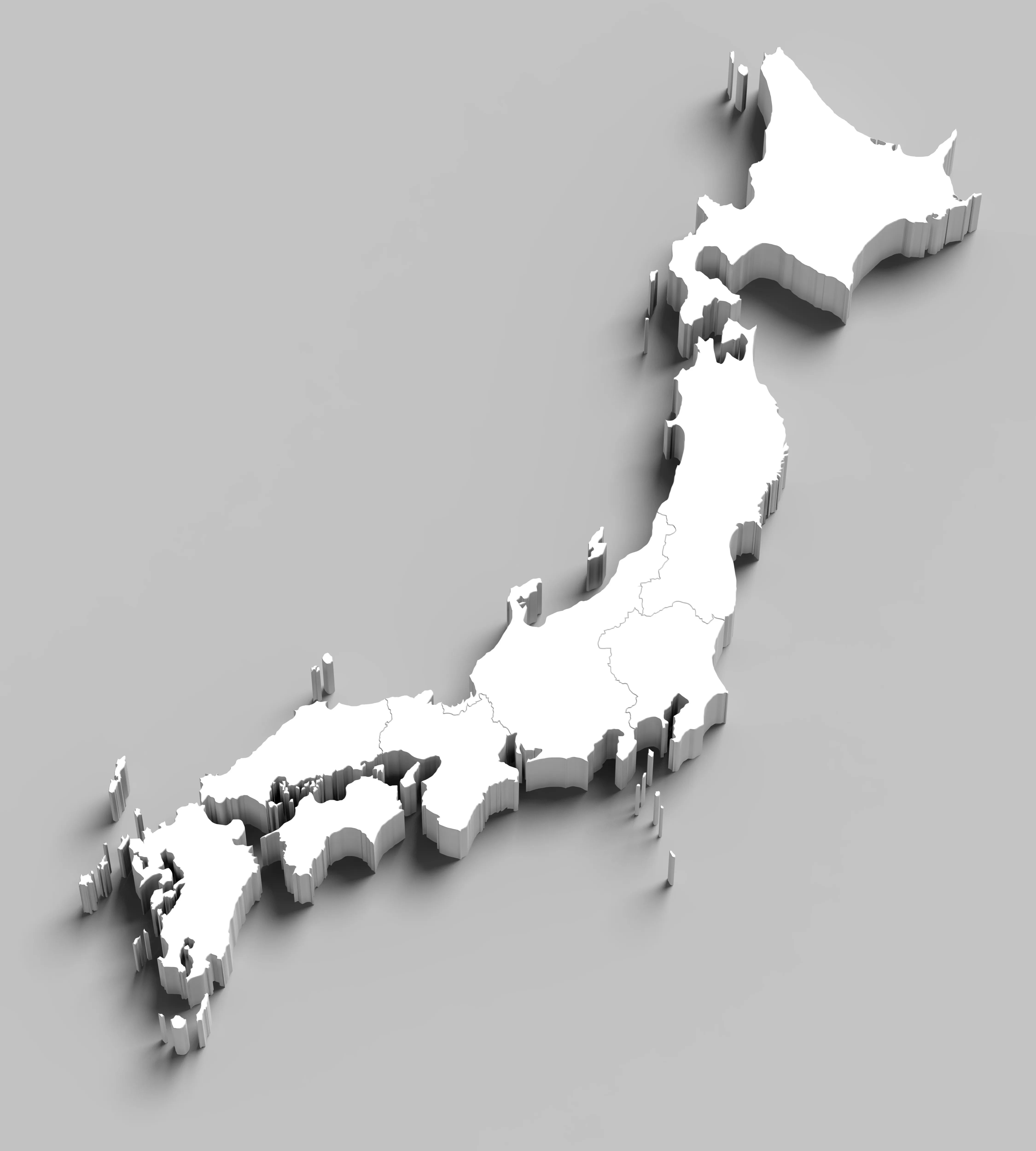
Kyushu, the third largest island in Japan, is home to the semiconductor production bases of integrated device manufacturers (IDMs) with world-class cutting-edge technology. SONY, Toshiba, Hitachi, Mitsubishi, Fujitsu and Nissan are among the sector’s shining stars, though a host of other IDMs tied to the supply chains of other major enterprises have also set root in Kyushu. Collectively, the companies earned Kyushu the name Silicon Island of Japan.Kyushu’s flourishing IDM industry sprouted from favorable tax and other government policies that reduced semiconductor production costs to levels lower than elsewhere in Japan. Once the IC producers had established bases, equipment and materials companies naturally followed, leading to the influx of many parts manufacturers. Together, they came to Kyushu, one after another, to make the island a magnet for manufacturing. And so it was to Kyushu that a SEMI China delegation travelled for a meeting at TEL’s factory in Kumamoto to learn more about the secrets to the rapid growth of the island’s semiconductor industry and promote cooperation between Chinese and Japanese enterprises. Underscoring the rise of the Silicon Island of Japan, China will soon become TEL’s largest market, said Masami Akimoto, Chairman of Tokyo Electron Kyushu Limited, speaking at the event. Masami Akimoto hopes for support from SEMI China.The island of 12 million people contributes to the growth of the global semiconductor industry, expected to reach USD 500 billion in size in 2019 as China’s semiconductor sector, fueled in part by government-backed investment funds, continues its rapid expansion. Despite the gains, China still lags other regions in advanced manufacturing, said Lung Chu, president of SEMI China, which is doing its part to draw more advanced manufacturing to the region through its SIIP platform. The initiative encourages pan-regional cooperation with China’s semiconductor industry to promote free trade, open markets, technology innovation and IP protection – all to help China better integrate with the global semiconductor industry. SEMI China President Lung Chu(L) issues visit memorial to Masami Akimoto(R), Chairman of Tokyo Electron Kyushu Limited. Chicken shall be led by the HenUnlike other regions with comprehensive semiconductor industries, Kyushu’s is primarily focused on production and assembly, with more than 200 manufacturers of semiconductor equipment and parts.SEMI China Delegation at Tokyo Electron Kyushu LimitedTEL built its first factory in Kumamoto, a city covered by volcanic ash in the center of Kyushu, 34 years ago. Today, TEL every month produces 80 to 90 sets of equipment, each consisting of, on average, over 400 thousand parts that must be certified and authorized by TEL before delivery to its module manufacturers and assembly into complete machines. Having blossomed over the past few decades, the island’s supply chain now supplies TEL with all its equipment parts. SEMI China Delegation at Fajita WorksTEL supplier Fajita Works, a high-precision plate metal manufacturer founded in 1945, is emblematic of other companies in the Kyushu supply chain. It keeps a low public profile as it serves several longtime customers and earns ardent loyalty from its workers, an ethos reflected in the change next January of its slog from “Only One” to “Great company, Great life.”Quality is the life of the enterpriseLong before the rise of its legendary automobile and consumer electronics companies, Japan was known for inferior, counterfeited products, labeled “Made In USA” and shipped to the United States by more than 100 factories. The net effect was to shrink and commoditize American markets. The tide in Japan’s product quality and stained reputation began to turn in the 1980s, when Japan’s semiconductor industry began to produce memory with an error rate 27 times lower than its U.S. competitors, giving Japan an upper hand in quality that it would never relinquish. SEMI China Delegation at HORIBAKyushu-based flowmeter supplier HORIBA, among the many Japanese companies famous for their product quality, ships 38 percent of its products into the automotive market and 27 percent into the semiconductor sector. Cleanliness is as vital a part of the company’s culture as quality. Each depends on the other, with fine detail held to the highest importance. On its visit to HORIBA, the SEMI China delegation, passing by an office area before entering the factory, sighed at the sight of the spotless, neatly kept furniture and workspace: They had never seen an office so sparkling clean. HORIBA’s success is rooted in immaculate offices, factories and the company’s motto “Enjoy innovation and pay close attention to product quality.”After Kumamoto sustained heavy damage during a 2016 earthquake, HORIBA workers returned rocks scattered by temblor to their original position, knowing that order is critical to lean, efficient manufacturing and that, indeed, “the devil is in the details.” SEMI China Delegation in Kumamoto City Full confidence in the exploration of Chinese marketConsumer electronics stalwarts Sony and Panasonic feature semiconductor factories in Kagoshima, the southernmost city in Kyushu and Japan, though rumor had it two years ago that Panasonic planned to pull out. The Panasonic plant, which provides batteries for Tesla, remains. The Sony facility produces image sensors for the iPhone.Semiconductor equipment maker ULVAC, SEMI China’s most important strategic partner, is also based in Kagoshima. During the delegation’s visit to the company, Lung Chu noted that while China is the world’s largest semiconductor market, the region meets just 13 percent of domestic chip demand. Stressing that ULVAC can play a crucial role in helping China become a bigger player, he expressed admiration for ULVAC’s professionalism along with hope that it will maintain its rapid growth and leverage SEMI resources to catalyze rapid development of Internet of Things (IoT), artificial intelligence (AI), and 5G technologies in China and rise into the top 10 of global equipment manufacturers. SEMI China President Lung Chu (L) issues visit memorial to ULVAC Kyushu President and CEO Kenji Yamaguchi ULVAC Kyushu president and CEO Kenji Yamaguchi made clear the company’s interest in Lung Chu’s insights into Chinese semiconductor industry while underscoring its core competency of producing semiconductors for flat panel displays. The Kyushu Factory of ULVAC is full of vitality and market competitiveness. SEMI China Delegation at ULVAC EBARA, a precision machinery company located in Kumamoto, has manufactured chemical-mechanical planarization (CMP) equipment for over 20 years and delivered nearly 2,400 mechanical polishing machines worldwide. While the company expects to ship 50 sets per year to China starting next year, it has the capacity to deliver 20 sets per month, enough to meet demand of Chinese semiconductor makers. SEMI China Delegation at EBARAThe most telling takeaway from the SEMI China delegation’s visit to the Kyushu: Japan ranks number one worldwide in research and development (R D) investment as a proportion of GDP and is also at the top in the percentage of R D funds controlled by private enterprises. The outsize investment strategy has enabled Japan to maintain its hold as one of the world’s top technology innovators.Like Sakurajima, the famed Kyushu volcano, the SEMI China delegation will continue to harness its forces to build relationships with the island’s semiconductor supply chain as it works to develop win-win pan-regional relationships and foster the growth of China’s semiconductor industry. Best view of Sakurai volcano Gang Yao is a marketing director at SEMI China.
Read More
Last week, the Office of the U.S. Trade Representative (USTR), on instruction from President Trump, notified Congress that the administration intends to begin bilateral trade negotiations with Japan, the European Union (EU), and the United Kingdom.SEMI stands strong for free trade and open markets, and roundly supports efforts to increase market access and tap into more foreign economies, especially economies like Japan and the EU, both of which are central to the semiconductor industry. The semiconductor industry, which enables the $2 trillion electronics market, is built on global commerce. SEMI members rely on a vast network of supply chains that span the globe, bringing together components and tools made all around the world and assembled into a single sub-system that is then integrated into a larger tool used in the chipmaking process.These free trade agreements will reduce tariffs, which will result in cost savings and productivity gains, and allow SEMI members to expand and grow. But the benefits of modern free trade agreements extend well beyond tariff reduction. Indeed, these trade deals will establish and enhance global trade rules that enable companies to innovate and compete fairly on a level playing field. Trade agreements strengthen certainty and further business continuity.While the exact nature and negotiation timelines for the talks remain unclear, SEMI will engage the administration, urging it to maintain high standards in these agreements, such as: Maintain strong respect for intellectual property and trade secrets through robust safeguards and significant penalties for violators Remove tariffs and non-tariff barriers on semiconductor products as well as products that depend on semiconductors Simplify and harmonize the customs and trade facilitation processes Combat any attempts of forced technology transfer Prevent use of data localization measures and enable the free flow of cross-border data flows End discriminatory and/or burdensome regulatory practices Ensure standards in all forms are market-oriented Create rules for state-owned enterprises to ensure fair and non-discriminatory treatment of all companies According to Trade Promotion Authority (TPA), the U.S. law that guides trade votes in Congress, negotiations with each country can only begin 90 days after last week’s notification. During that period, there will be intensive consultation with Congress and stakeholders. This means, at the earliest, talks can start on January 14, 2019. (Bear in mind that discussions with the UK can only begin in earnest once the UK has formally left the European Union on March 29, 2019.)The Trump administration’s announcement comes after the U.S. imposed or threatened tariffs on imports on all trading partners, including the EU and China. All told, the U.S. has imposed tariffs on more than $300 billion worth of goods. SEMI has weighed in on the detrimental nature of tariffs, arguing that tariffs on China will ultimately do nothing to address the concerns with China’s trade practices. This sledgehammer approach will introduce significant uncertainty, impose greater costs, and potentially lead to a trade war, ultimately undercutting the ability of semiconductor companies to sell overseas, stifling innovation and curbing U.S. technological leadership.Elsewhere, the Comprehensive and Progressive Agreement for Trans-Pacific Partnership, the multilateral trade deal that links 11 Asia-Pacific economies, is well on its way to taking force. Canada will be taking its final steps to ratify the deal, joining Mexico, Japan and Singapore. The deal, formerly known as the Trans-Pacific Partnership, should take effect by the first half of 2019.SEMI will continue tracking ongoing trade developments. Any SEMI members with questions should contact Jay Chittooran, Public Policy Manager at SEMI, at [email protected].
Read More
Last week, more than a dozen senior semiconductor executives traveled to Washington, DC for the first-ever Fall Washington Forum. The SEMI Washington Forum, a venue for SEMI members to educate lawmakers about the industry, focused on action against China, both in the form of tariffs and export controls.Our industry is global, and companies rely heavily on trade. In 2017, more than 90 percent of equipment made in the United States was exported. Because of this dynamic, the United States holds a nearly $9 billion trade surplus in this industry. SEMI supports trade policies that open foreign markets. In the meetings, the executives expressed deep concern that the tariffs would inflict deep damage to the U.S. economy, including to SEMI members. Estimates suggest that the Sec. 301 tariffs (and the Chinese retaliatory tariffs) will cost semiconductor companies more than $700 million annually, dramatically increasing the cost of doing business. These tariffs also threaten U.S. technological leadership. The United States has led innovation for decades. However, by pursuing policies that limit market access opportunities, company-led R D and innovation will slow, which, in turn, will curb further export potential. SEMI companies also stressed that because of the blunt application of these tariffs, this action will actually hurt U.S. companies as much as it hurts their Chinese competitors. Indeed, about 40 percent of imports in our sector from China are from U.S. or other non-Chinese companies. Further, the semiconductor industry relies on a vast network of supply chains, which have been built and qualified over the course of years. A fundamental revamp of supply chains is simply not feasible. This would be expensive, time-consuming, and resource-intensive. With a growing number of policy issues that are central to and could have significant impact for semiconductor companies, SEMI hosted its first ever Fall Washington Forum for members of its North American Advisory Board (NAAB). SEMI also invited several other industry executives. In total, 14 senior industry executives, including representatives from equipment manufacturers, component suppliers, and materials providers, attended the Fall ForumDuring the two days of meetings, SEMI met with several senior Administration officials to better the policies being enacted and considered as well as encourage all parties to not impose barriers to commerce, which would severely impact the semiconductor industry. SEMI also met with Members of Congress and their staffs on this issue. All told, attendees at the Fall Forum had more than 15 meetings with policymakers, reflecting the great impact of public policy on SEMI members companies. At a time when the stakes for the industry could not be higher, direct engagement with lawmakers is critical. The Washington Forum offers an incredible opportunity for members to better understand the impact of key public policy issues and gain firsthand experience in influencing policy and helping lawmakers better understand the industry.If you are interested in learning more about the SEMI Washington Forum or SEMI’s public policy program, please contact Jay Chittooran by email at [email protected].
Read More
IntroductionStarting July 4, 2022, PFOA (Perfluorooctanoic acid) levels in semiconductor manufacturing and related equipment (SMRE), including replacement parts, entering the European Union (EU) will be restricted to 25 ppb per component (or any part thereof). Semiconductor equipment components (and the parts thereof) of particular concern include fluid tubing and fittings, pipe/seal tape, wire and cable insulation, filters, valves, tanks, panels, reaction vessels and o-rings; if they are made from fluoropolymers or fluoroelastomers.When PFOA is used as an aid to the manufacture fluoropolymers such as PTFE, PFA, PVDF or fluoroelastomers such as FKM and FFKM (collectively referred to as fluoromaterials), an unintended PFOA residue can be trapped within the fluoromaterial. Buyers of components used in SMRE are usually unaware of the processing method used for any fluoromaterials they may contain, and, as a consequence, the potential for PFOA residue. This lack of information about potential PFOA residues could result in regulatory enforcement actions and restricted market access, particularly in the EU.The impact of restrictions on fluoromaterials used in SMRE has been introduced in previous SEMI articles ‘Fluorinated Compound Restrictions May Trigger Costly Equipment Changes’ and ‘Fluorinated Substance Restrictions Triggers Costly Equipment Changes.’PFOA and its related compounds, such as the ammonium salt APFO (collectively called PFOA in this article), are recognized internationally as hazardous chemicals and are now targeted for regulatory restriction in the U.S., Taiwan, Canada and the EU. The UN Stockholm Convention on Persistent Organic Pollutants (POPs) is also considering listing PFOA, which could lead to additional international restrictions.The SEMI EHS Division PFOA Compliance Working Group has been working to understand: The likelihood of PFOA residue entering the supply chain of new components The residual level of PFOA in fluoromaterials produced prior to the phase out of PFOA by some manufacturers The impact of PFOA residue on the secondary equipment market This SEMI resource page, ‘Elimination of PFOA from the Equipment Supply Chain,’ and the supporting FAQ contain the Working Group’s key findings and conclusions.PFOA in the Fluoromaterial Supply ChainSignatories to the U.S. EPA Stewardship Program, which include FluoroCouncil members, eliminated PFOA from their manufacturing processes by 2013. However, other fluoromaterial manufactures – particularly in China, Russia and India – might still use PFOA and pose a significant risk to the worldwide supply chain.China, the world’s largest fluoromaterial producer, accounts for 53 percent of global production of PTFE and 38 percent of worldwide production of PVDF, FEP and FKM. An estimated 75 percent to 85 percent of fluoromaterials are manufactured using PFOA in China. Fully 25 percent of these fluoromaterials are exported, primarily to the U.S, Japan, EU and India. What’s more, finished goods made from or containing fluoromaterials that might be used as components in SMRE are exported from China.Documentation that traces fluoromaterials through the supply chain back to the original fluoromaterial manufacturer is key to meeting the PFOA regulatory requirements. This traceability can be straightforward in cases when an SMRE manufacturer directly specifies the use of a fluoromaterial in a custom-fabricated fluoromaterial component. However, for off-the-shelf components (e.g., cable ties, wiring insulation, tubing) or the components assembled from these components (e.g., controllers), the complexity and dynamics of the supply chain makes traceability back to the original fluoromaterial producer almost impossible.Residual PFOA Levels If, or how much, PFOA/APFO residue is contained in a fluoromaterial depends on the manufacturing process. Details of the manufacturing processes are proprietary and vary widely. Post manufacturing thermal treatments, such as sintering, extrusion, and molding, can result in the rapid thermal decomposition of APFO above 250C, but PFOA is significantly more stable. The temperature and time of thermal treatments is also proprietary and varies depending on the type of fluoromaterial and what is being made.This variability makes it impossible to estimate the likely level of trapped PFOA or APFO in a finished component or a part thereof. It is unwise to use data on the level of residue made known for one case to extrapolate the level of residue across the fluoromaterial industry. However, an industry-wide range on the order of 1ppm-10ppm (nearly 1000 times the EU limit) is suspected. Testing for the presence of PFOA/APFO at 25ppb in components is also problematic as there is no standard test method, and results among the custom methods developed in each test lab may vary.Given this uncertainty in test methods, a system of supplier declarations warrants consideration.Impact on Secondary (Used) EquipmentThe EU REACH restrictions apply to SMRE and replacement parts placed on the market at any time (not just initial placement – known as “first placing on the market”). For fluoromaterial components manufactured prior to 2013, there is a higher likelihood of residual PFOA/APFO levels exceeding the 25ppb limit of EU REACH. In principle all the SMRE components containing fluoromaterials should be investigated, and those containing PFOA above 25ppb must be replaced before the SMRE can be legally placed again on the EU market. Companies (e.g., semiconductor manufacturers) in the EU who wish to sell used equipment within the EU will be required to demonstrate the used equipment is in compliance. Selling older used equipment would likely be unprofitable after necessary investigations and component replacements are completed.Next StepsWhile the EU semiconductor manufacturing industry heavily depends on the secondary (used) equipment market, EU regulators may be unaware of the PFOA restriction’s damaging impact to this market. The EHS Division PFOA Working Group, in conjunction with SEMI Europe, is now considering how to bring this concern to the attention of regulators and to collaborate and lobby for effective changes including possible modifications to the EU Persistent Organic Pollutants (POPs) regulation.
Read More