downloadGroupGroupnoun_press release_995423_000000 copyGroupnoun_Feed_96767_000000Group 19noun_pictures_1817522_000000Member company iconResource item iconStore item iconGroup 19Group 19noun_Photo_2085192_000000 Copynoun_presentation_2096081_000000Group 19Group Copy 7noun_webinar_692730_000000Path
Skip to main content
Default Banner Image

Japan

Environmentally sound policies and the health and the safety of workers in the microelectronics supply chain are vitally important to SEMI and its members. For more than two decades, together we have focused on worker safety by focusing on global environment, health and safety (EHS) compliance and regulatory issues and the advancement of sound EHS practices. Today, EHS has taken on an even higher profile in the microelectronics industry with its growth across Europe, North America and Asia. Never has the industry been under greater scrutiny. The list of regulatory agencies is growing. To keep pace with rising EHS requirements and continue to ensure worker safety, we’d like your help. The SEMI EHS summit will open with a keynote presentation from Russ LaMotte, Managing Principal of Beveridge Diamond, and a recognized expert on EHS issues in the electronics industry. Member companies representing equipment, materials, facilities and devices will then each share their EHS concerns. Finally, working groups will address industry EHS challenges and gaps. Outputs from the working group meetings will form the basis for the future SEMI EHS program. The EHS issues SEMI’s program and company volunteers are addressing include: PFOA – Government efforts to eliminate pefluoro-octanoic acid and related compounds and salts (collectively known as PFOA) from company supply chains REACH – A European Union regulation to strengthen protections against chemical risks to human health and the environment. Other countries – Japan, Korea, Taiwan – have enacted similar regulations. Stockholm Convention – An international environmental treaty designed to eliminate or restrict the production and use of persistent organic pollutants (POPs) Waste Framework Directive Database – The European Commission and the European Chemicals Agency (ECHA) are building a database where all suppliers will be required to register certain articles. Other groups are dealing with country-specific aspects of the Restriction of Hazardous Substances (RoHS) and the Toxic Substances Control Act (TSCA). Complementing our advocacy efforts, SEMI has established 25 primary EHS standards with SEMI S2 (Safety) as the cornerstone. The S2 family of SEMI Standards acts as performance-based EHS considerations for semiconductor manufacturing equipment and has also been adopted by adjacent industries. Sign up for the November 29th SEMI EHS Summit today Team up with your SEMI colleagues to collectively formulate the semiconductor manufacturing industry’s EHS program. SEMI members can register for the November 29th SEMI EHS Summit by clicking here. If you cannot make this meeting but wish to be added to SEMI’s regular communication on EHS and Advocacy issues, please click here and choose Advocacy from the list of topic choices. Michael Ciesinski is vice president of the FlexTech Alliance, a SEMI Strategic Association Partner chartered with building up infrastructure for flexible electronics manufacturing.
Read More
Last week, the Office of the U.S. Trade Representative (USTR), on instruction from President Trump, notified Congress that the administration intends to begin bilateral trade negotiations with Japan, the European Union (EU), and the United Kingdom.SEMI stands strong for free trade and open markets, and roundly supports efforts to increase market access and tap into more foreign economies, especially economies like Japan and the EU, both of which are central to the semiconductor industry. The semiconductor industry, which enables the $2 trillion electronics market, is built on global commerce. SEMI members rely on a vast network of supply chains that span the globe, bringing together components and tools made all around the world and assembled into a single sub-system that is then integrated into a larger tool used in the chipmaking process.These free trade agreements will reduce tariffs, which will result in cost savings and productivity gains, and allow SEMI members to expand and grow. But the benefits of modern free trade agreements extend well beyond tariff reduction. Indeed, these trade deals will establish and enhance global trade rules that enable companies to innovate and compete fairly on a level playing field. Trade agreements strengthen certainty and further business continuity.While the exact nature and negotiation timelines for the talks remain unclear, SEMI will engage the administration, urging it to maintain high standards in these agreements, such as: Maintain strong respect for intellectual property and trade secrets through robust safeguards and significant penalties for violators Remove tariffs and non-tariff barriers on semiconductor products as well as products that depend on semiconductors Simplify and harmonize the customs and trade facilitation processes Combat any attempts of forced technology transfer Prevent use of data localization measures and enable the free flow of cross-border data flows End discriminatory and/or burdensome regulatory practices Ensure standards in all forms are market-oriented Create rules for state-owned enterprises to ensure fair and non-discriminatory treatment of all companies According to Trade Promotion Authority (TPA), the U.S. law that guides trade votes in Congress, negotiations with each country can only begin 90 days after last week’s notification. During that period, there will be intensive consultation with Congress and stakeholders. This means, at the earliest, talks can start on January 14, 2019. (Bear in mind that discussions with the UK can only begin in earnest once the UK has formally left the European Union on March 29, 2019.)The Trump administration’s announcement comes after the U.S. imposed or threatened tariffs on imports on all trading partners, including the EU and China. All told, the U.S. has imposed tariffs on more than $300 billion worth of goods. SEMI has weighed in on the detrimental nature of tariffs, arguing that tariffs on China will ultimately do nothing to address the concerns with China’s trade practices. This sledgehammer approach will introduce significant uncertainty, impose greater costs, and potentially lead to a trade war, ultimately undercutting the ability of semiconductor companies to sell overseas, stifling innovation and curbing U.S. technological leadership.Elsewhere, the Comprehensive and Progressive Agreement for Trans-Pacific Partnership, the multilateral trade deal that links 11 Asia-Pacific economies, is well on its way to taking force. Canada will be taking its final steps to ratify the deal, joining Mexico, Japan and Singapore. The deal, formerly known as the Trans-Pacific Partnership, should take effect by the first half of 2019.SEMI will continue tracking ongoing trade developments. Any SEMI members with questions should contact Jay Chittooran, Public Policy Manager at SEMI, at [email protected].
Read More
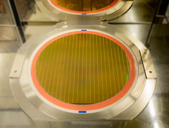
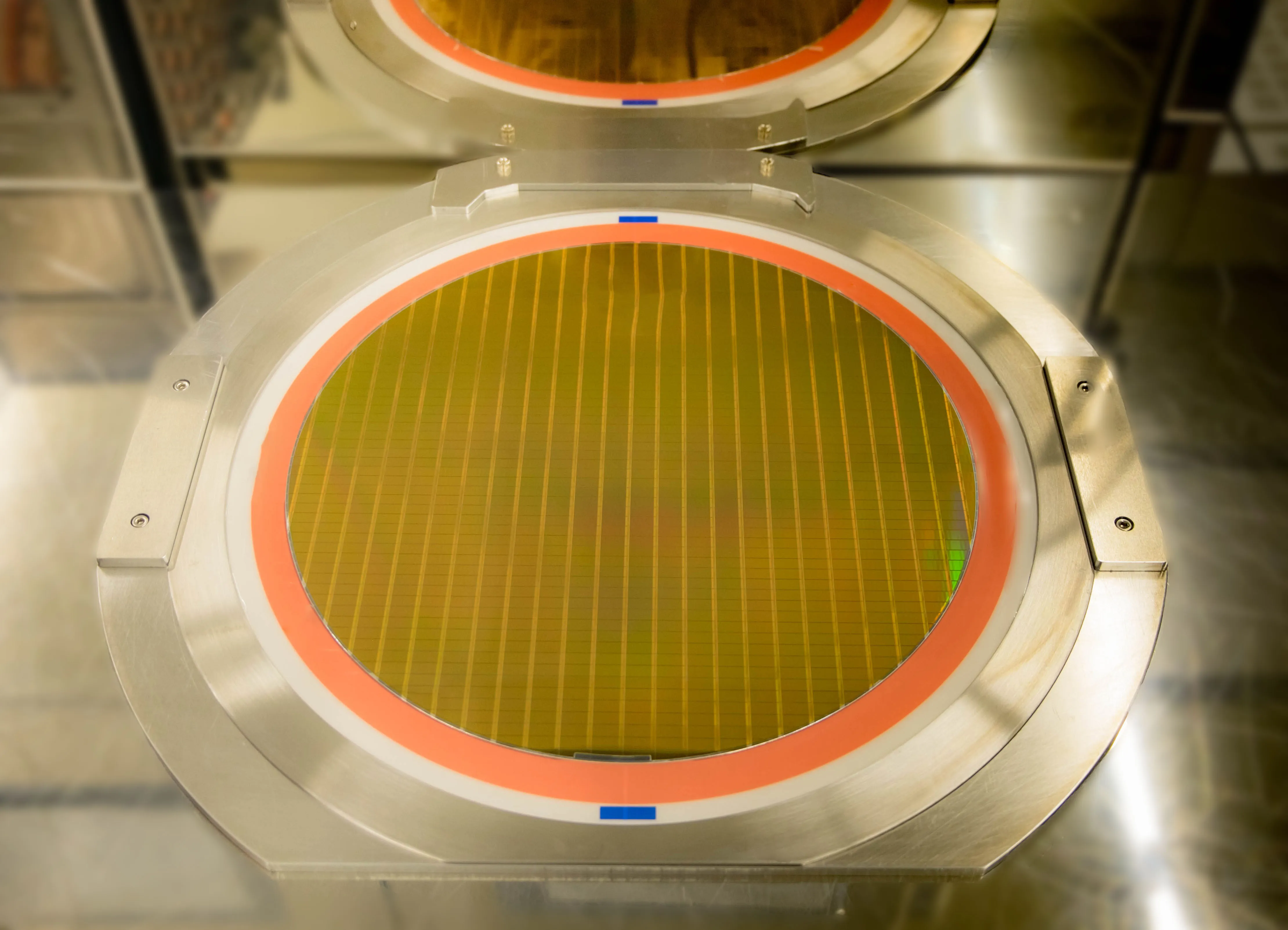
On June 1st, 2018, Toshiba sold Toshiba Memory, Toshiba’s memory business, to an investment group led by Bain Capital. Toshiba Memory was then owned by a consortium of American, Japanese and Korean companies.After the long and tough negotiations, Toshiba Memory moved forward at full throttle, holding a groundbreaking ceremony for its new 3D NAND fab (100,000 WPM) in Kitakami in July and, in September, celebrating the opening of Fab 6 Phase 1 (50,000 WPM). To be sure, NAND memory is a key feature of Japan’s semiconductor industry. But the sector’s reach extends well beyond memory with its rich and versatile product portfolio nourished by active investment.Born in the early 1950s, Japan’s semiconductor industry today boasts more than 30 companies with fabs. Many feature 200mm and smaller wafer lines with legacy technologies, form factors that account for the bulk of the world’s semiconductors and are the oxygen of Japan’s chip industry. Clearly, the world is not built only with the state-of-art 7nm processed chips on the latest generation 300mm lines. Japanese chipmakers are flourishing.Automotive SemiconductorsRenesas Electronics remains a giant in microcontrollers (MCU) and system on chip (SoC) devices for automotive applications. According to IHS Markit, Renesas automotive semiconductor revenue in 2017 reached $3.6 billion while Inineon Technologies and NXP Semiconductors revenues were $3.4 billion and $3.7 billion, respectively. The three companies dominate the global automotive MCU global market. The company recently acquired Integrated Device Technology (IDT), a U.S. fabless company specializing in analog/mixed signal chips, to strengthen its automotive semiconductor portfolio. Renesas operates four volume production fabs, according to the latest World Fab Forecast from SEMI. Renesas’s microcontrollers for automotive applications (Source: Renesas Electronics) Power SemiconductorsWith power semiconductors the chips of choice for boosting the efficiency and performance of motors and batteries used in equipment, demand for the devices is rapidly growing, especially for automotive applications. Power semiconductor companies in Japan are legion and include Denso, Fuji Electric, Fujitsu Semiconductor, Hitachi, Kyocera, Mitsubishi Electric, New Japan Radio, Origin Electric, Phenitec Semiconductor, Renesas, Rohm, Sanken Electric, Sansha Electric Manufacturing, Seiko NPC, Shindengen Electric Manufacturing, Sumitomo Electric Device Innovations, Toshiba and Toyota Industries. The companies account for 26% of global power semiconductor capacity and will spend $317 million for construction and equipping in 2018.CMOS SensorsSony dominates the CMOS image sensors market with 42% share in 2016, according to Yole Développment. To meet growing demand for high-end CMOS image sensors, Sony has acquired several legacy 300mm wafer fabs and retooled them for CMOS sensor manufacturing. What’s more, Sony’s May announcement of its mid-term corporate strategy includes a 1 trillion Japanese yen investment in CMOS image sensors targeted to automotive applications by March 2021.Sony’s 7.42 effective megapixel stacked CMOS image sensor for automotive cameras (Source: Sony Corporation) MEMSMEMS is perhaps the most wide-ranging device market: Every application requires different capabilities and functions. The latest World Fab Forecast report lists 17 MEMS companies in Japan, though three makers of fast-growing RF MEMS, typically known as surface acoustic wave (SAW) or bulk acoustic wave (BAW) filters, are coming to the attention of semiconductor manufacturers. All are familiar passive electronic components suppliers – Murata Manufacturing, Taiyo Yuden and TDK – and all acquired legacy semiconductor fabs to manufacture RF MEMS.Their high-performance radio wave filters make mobile phones usable around the world. Research companies like Yole expect the introduction of 5G cellular mobile communication systems to fuel another wave of growth of the RF MEMS market. Murata Manufacturing’s SAW filters for smart phones (source Murata Manufacturing) Japanese Supply Chain Meets All Different NeedsJapan’s semiconductor supply chain provides one third of the world’s semiconductor manufacturing equipment and more than half of the industry’s materials. But Japanese suppliers also work with small and midsize makers of highly versatile chips critical to enabling the explosion of smart applications.Meet these versatile Japanese suppliers at SEMICON Japan to find solutions to your unique needs and help the world get smarter. Themed “Dreams Start Here,” SEMICON Japan 2018 reflects the promise of AI (artificial intelligence), Internet of Things (IoT) and Smart technologies. Featuring more than 750 exhibitors from around the world, the event is the gathering place to connect the people, technologies and business across the electronics manufacturing supply chain, from semiconductor manufacturing to autonomous cars, robotics and other smart applications. For more information about SEMICON Japan, visit www.semiconjapan.org.Yoichiro Ando is a marketing director at SEMI Japan.
Read More
The Japan semiconductor manufacturing supply chain is a global semiconductor industry workhorse, producing about one third of world’s chip equipment and more than half of its semiconductor materials. In contributing the vast majority of these products, SEMI Japan member companies hold the high distinction of enabling continuous development of the worldwide semiconductor industry. Aptly, then, technology powerhouses IBM, Nissan Motors and Toshiba offered insights into the latest trends and innovations in computing and smart cars at the late-May SEMI Japan Members Days in Tokyo with 133 technologists from member companies in attendance. As the audience discovered, chip innovation never sleeps and, as futuristic as it can be, invariably gives rise to possibilities beyond the human imagination. That was the message of kickoff presentation “Computing Reimagined – AI/Quantum/IoT” – by Dr. Shintaro Yamamichi, Senior Manager, Science Technology at IBM Research-Tokyo. Dr. Yamamichi cited three examples of how semiconductors uncover new technology frontiers. Computational materials discovery, a novel methodology, is the application of theory and computation to unearthing new materials and the key to enabling an ongoing stream of semiconductor innovation. In particular, using cognitive technology to mine huge volumes of literature reveal new insights into materials that uncover even more functionality such as greater conductivity and heat resistance. With new materials the oxygen of ever more advanced semiconductor chip manufacturing, the semiconductor industry will surely benefit from this methodology. The opportunity to accelerate quantum computing innovation is now. Launched in May 2016, the IBM Quantum Experience gives students, researchers and general science enthusiasts hands-on access to IBM’s experimental cloud-enabled quantum computing platform. The online platform features a forum for discussing quantum computing topics, tutorials on how to program IBM Q devices, and other educational material about quantum computing. Dr. Yamamichi encouraged the audience to join the program. The world’s tiniest computer, unveiled by IBM at the company’s Think 2018 conference in Las Vegas, packs several hundred thousand transistors and, IBM claims, the equivalent power of a 1990s x86 chip into a package smaller than a grain of salt. The computer’s small form factor (less than 1mm x 1mm) and low manufacturing cost means it can be embedded in product price tags and packages as an anti-fraud device using blockchain technology. Vehicles need to be both electric and intelligent as countries become more populous and traffic density increases. More drivers extend average drive time, boost greenhouse emissions, devour precious energy resources and lead to more traffic congestion and accidents. Dr. Haruyoshi Kumura, fellow at Nissan Motor, highlighted these issues in stressing the importance of a new era of intelligent mobility. To mitigate these problems, Nissan is focusing on the electrification and intelligence of its vehicles: Nissan’s electric vehicle, Leaf, reduces accidents with electric intelligence systems such as e-Pedal, which uses an accelerator pedal only for both acceleration and deceleration, and ProPILOT Park, a feature that automatically parks the car by using multiple cameras and ultrasonic sonars to detect pedestrians and other objects around the vehicle. With more than 90 percent of traffic accidents caused by driver error, Nissan plans to introduce autonomous driving on multi-lane highways by the end of 2018 and on city streets by 2020. By 2022, the company plans to roll out full autonomous driving to reduce traffic accidents caused by inattentive drivers. For full autonomous driving to materialize, sensor fusion technology must incorporate a combination of technologies – radar systems, light detection and ranging (LiDAR) systems and cameras – to identify the shapes and locations of nearby moving objects and measure their speed. Sensed information is then processed by a 3D graphic analyzer to make electric throttle, braking and steering decisions. The outlook for automotive industry includes car sharing and more electrification – both insights from Yoshiki Hayakashi, general manager, automotive solution strategic planning division at Toshiba Electronic Devices Storage, who offered his perspectives on trends in Japan’s automotive industry and beyond. To meet the requirements of the COP21 Paris agreement, the global automotive industry is shifting to electrification. Toshiba estimates 60 percent of new cars will be electric vehicles by 2040 to meet the International Energy Agency’s global EV outlook. In Japan, autonomous driving or advanced driver assistance systems (ADAS) will be offered in certain areas by 2020, the year of the Tokyo Olympic games. Growth of these advanced driving systems hinges on infrastructure development. Supporting data centers, intelligent transport systems, vehicle-to-everything connections, and smart city are all necessary components. Car ownership will begin to cede ground to car sharing with technology elites such as Tesla, Apple and Google leading the way. To expand the car-sharing industry, new alliances will take shape between new and old-guard automotive companies and electronics manufacturing services (EMS) providers. Autonomous driving requires precise 3D renderings of actual roadways using sensors for route mapping. While sensor fusion must be deployed for these capabilities, LiDAR offers better sensing range and space resolution precision than ultrasonic sonars, radars, and cameras. The next SEMI Japan members day is scheduled for October 30 in Tokyo. SEMI holds similar events in most regions where SEMI and its members operate. For the members events in your region, contact the SEMI office nearest you. Yoichiro Ando is a marketing director in SEMI Japan.
Read More
Storage and memory chipmaker and SEMI China member Tsinghua Unigroup is gearing up to meet burgeoning product demand with huge investments in its manufacturing plants. But the high-tech enterprise under Tsinghua University is eyeing a much bigger prize – growth of the region’s semiconductor industry and the realization of its ambition to become a more prominent force on the global stage.Inspired by the national strategy, the Tsinghua Unigroup’s big spends include USD 24 billion in Wuhan (Yangtze Memory Technologies Co., Ltd.,) USD 30 billion in Chengdu, USD 30 billion in Nanjing and USD 100 billion in Chongqing, said Liu Hongyu, senior vice president of Tsinghua Unigroup, speaking at the SEMI China Equipment and Materials Committee meeting last month.Advanced packaging is another rich vein of opportunity the region is tapping for expansion, said Liu Hongjun, vice president of China Wafer Level CSP Co., Ltd., another SEMI China member attending the event, hosted by NAURA in Beijing. Hongjun sees strong growth for Fan-in, Fan-out, FCBGA, 2.5D and 3DIC, with Fan-out out front. Liang Sheng, administrative commission director at BDA, a business advisory firm supporting high-technology manufacturing in the E-Town economic development zone, pointed to 5G chips and smart, networked electric automobiles as drivers of the next growth phase of Beijing’s integrated circuit (IC) industry.Global tailwinds are lifting China’s semiconductor industry and the region’s hopes, with SEMI and major industry analysts raising their semiconductor industry growth projects for 2018 to between 9 percent and 16 percent. According to SEMI’s latest market report, global semiconductor industry manufacturing equipment revenue reached USD 17 billion in the first quarter of 2018, logging all-time highs after jumping 12 percent from the previous quarter and 30 percent year-over-year. Korea was the top-performing region at USD 6.26 billion, followed by China at USD 2.64 billion.Tighter integration with the rest of the global semiconductor industry is critical to the growth of China’s chip sector, and SEMI China is squarely focused on this assimilation, said SEMI China president Lung Chu. The spearhead of this effort is the SEMI Innovation Investment Platform (SIIP) China, established by SEMI China last year to help grow China’s pool of skilled workers, promote advanced technology, generate industry capital, and expand China’s semiconductor industry while developing stronger connections with chip sectors in other regions. To strengthen ties with other regions, SIIP China will stage a number of innovation and investment forums this year including Chinese Night at SEMICON West (July 10-12) and a SIIP China Forum in Silicon Valley (July 15). In August, representatives from the Korea chip industry will visit counterparts in China (August), and a China delegation will travel to Japan for meetings (October). SIIP China is also strengthening the region’s links with Germany and Israel as SEMI serves as a crucial bridge between China’s semiconductor sector and the global industry.At the invitation of Shanghai authorities and the Ministry of Commerce of the People’s Republic of China, SEMI China in November will join the China International Export Import Exposition in Shanghai, an event that will underscore China’s commitment to the openness and cooperation of its semiconductor industry with the international chip community. As part of the exposition, SEMI will work with the Ministry of Commerce and domestic chip manufacturers to begin development of a special integrated circuit (IC) zone. SEMI China members are welcome to participate.With workforce development no less vital to the future of China’s semiconductor industry, the Equipment Materials Committee offered potential solutions to the industry’s talent gap. Measures included targeting university students and engineers with industry lectures and courses in key cities, campus recruiting, talent training that members said they are willing to help SEMI coordinate and stage and, much like the push to better integrate China with the global semiconductor industry, mobilizing member resources around a campaign to polish the image of the industry to make it more attractive to students and young workers. Members of the SEMI China Equipment Material Committee gathered at NAURA in Beijing in June for a warm and lively discussion about global semiconductor industry cooperation and growing China’s semiconductor sector.Cherry Sun is a marketing manager at SEMI China.
Read More
Christian G. Dieseldorff, Industry Research Statistics Group, SEMI (June 12, 2018)The semiconductor industry is nearing a third consecutive year of record equipment spending with projected growth of 14 percent (YOY) in 2018 and 9 percent in 2019, a mark that would extend the streak to a historic fourth consecutive growth year, according to the latest update of the World Fab Forecast report published by SEMI. The industry last saw four consecutive years of equipment spending growth in the mid 1990s.Korea and China are leading the growth, with Samsung dominating global spending and ascendant China on a fast, steep rise, surging ahead of all other markets. See figure 1.Figure 1: equipment spending by region (includes new and refurbished)Samsung is expected to reduce equipment investments in 2018. Despite the ebb, the company still accounts for a dominant 70 percent of all investment in Korea. At the same time, SK Hynix is increasing its equipment spending in Korea.China’s equipment spending is forecast to jump a whopping 65 percent in 2018 and 57 percent in 2019. Notably, 58 percent of investments in China in 2018 and 56 percent in 2019 stem from companies with headquarters in other regions such as Intel, SK Hynix, TSMC, Samsung, and GLOBALFOUNDRIES. Domestic, Chinese-owned companies – backed by large government initiatives – are building an impressive number of new fabs that will start equipping in 2018. The companies will double their equipment investments in 2018 and again in 2019.Meanwhile, other regions are also ramping up investments. Japan is beefing up equipment spending by 60 percent in 2018, with the largest increases by Toshiba, Sony, Renesas and Micron.The Europe and Mideastern region will boost investments by 12 percent in 2018, with Intel, GLOBALFOUNDRIES, Infineon and ST Microelectronics as the largest contributors. Southeast Asia will increase investments by more than 30 percent in 2018, although total spending is proportionately smaller than in other regions owing to its size. The main contributors are Micron, Infineon and GLOBALFOUNDRIES, though companies including OSRAM and ams are also increasing investments.The SEMI World Fab Forecast, which also includes information on other companies, covers data and predictions through the end of 2019, including milestones, detailed investments by quarter, product types, technology nodes and capacities down to fab and project level.Learn more about the SEMI fab databases at:www.semi.org/en/MarketInfo/FabDatabase and www.youtube.com/user/SEMImktstats.
Read More
Thanks to you and the more than 5,000 other industry experts who contribute your time and brainpower, the SEMI Standards Program is celebrating its 45th anniversary in 2018. The first SEMI Standards meeting was held in 1973 to create a dimensional specification for silicon wafers. At the time, the proliferation of more than 2,000 different wafer specifications had led to major inefficiencies as the industry was just getting underway. To address this problem, wafer suppliers gathered under the auspices of SEMI and quickly developed consensus specifications for 2-inch wafers, and by the mid-1970s over 80 percent of wafers being shipped conformed to the new standard.Since that time, the SEMI Standards Program has expanded both geographically and technically. The program now has 20 technical committees in China, Europe, Japan, Korea, North America, and Taiwan, tackling manufacturing challenges across the electronics supply chain. Critical milestones include the development of SEMI S2, the comprehensive safety guideline that has drastically reduced industry incidents and continues to be updated to keep up with the hazards associated with semiconductor manufacturing, and the SECS/GEM and EDA suites of equipment communication standards, which are the backbone of modern day semiconductor “Smart Manufacturing.”As we commemorate our 45th year, there has never been a more diverse and active agenda as we look to solving issues in new areas such as Fan-Out Panel Level Packaging, Electron Microscopy Workflow, and flexible hybrid electronics. Of course, the Standards Program owes its success and longevity to you. I am repeatedly amazed by the dedication of Standards Members, and look forward to continuing the industry collaboration – together we can make the next 45 years as fun and productive as the first!As SEMI president and CEO Ajit Manocha has stated, “SEMI Standards is the oxygen of the industry.”SEMI Standards has saved the industry untold billions of dollars by defining interoperability specifications, guidelines and test methods that have streamlined semiconductor manufacturing and ensured the smooth operation of hundreds of pieces of equipment – all working automatically 24X7.What's more, SEMI Standards has enabled the production of more than 2.2 billion wafers and 1.8 trillion IC devices. Referenced more than 10 million times in production fab purchases, more than 25 SEMI Standards, on average, are cited in each purchase order for semiconductor equipment and materials in the electronic manufacturing ecosystem.
Read More