downloadGroupGroupnoun_press release_995423_000000 copyGroupnoun_Feed_96767_000000Group 19noun_pictures_1817522_000000Member company iconResource item iconStore item iconGroup 19Group 19noun_Photo_2085192_000000 Copynoun_presentation_2096081_000000Group 19Group Copy 7noun_webinar_692730_000000Path
Skip to main content
Default Banner Image

semiconductors

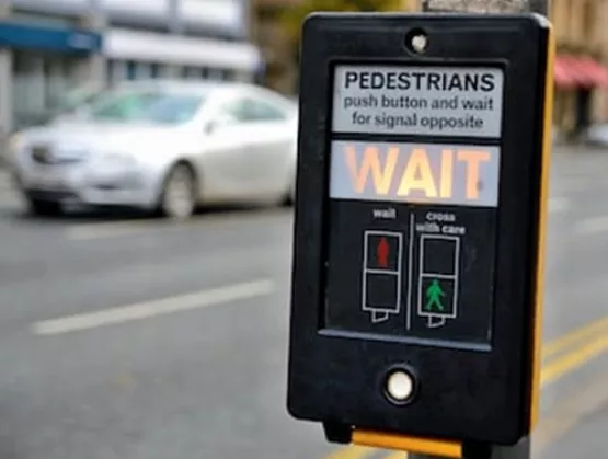
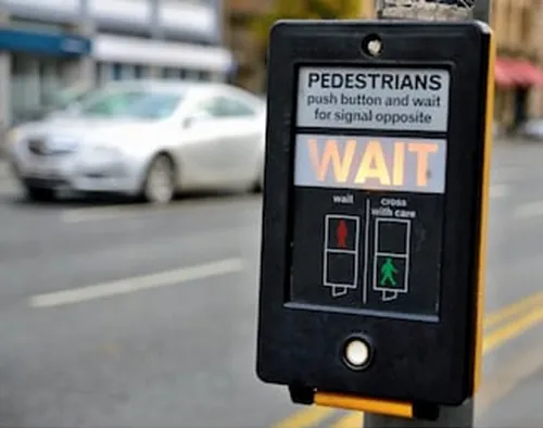
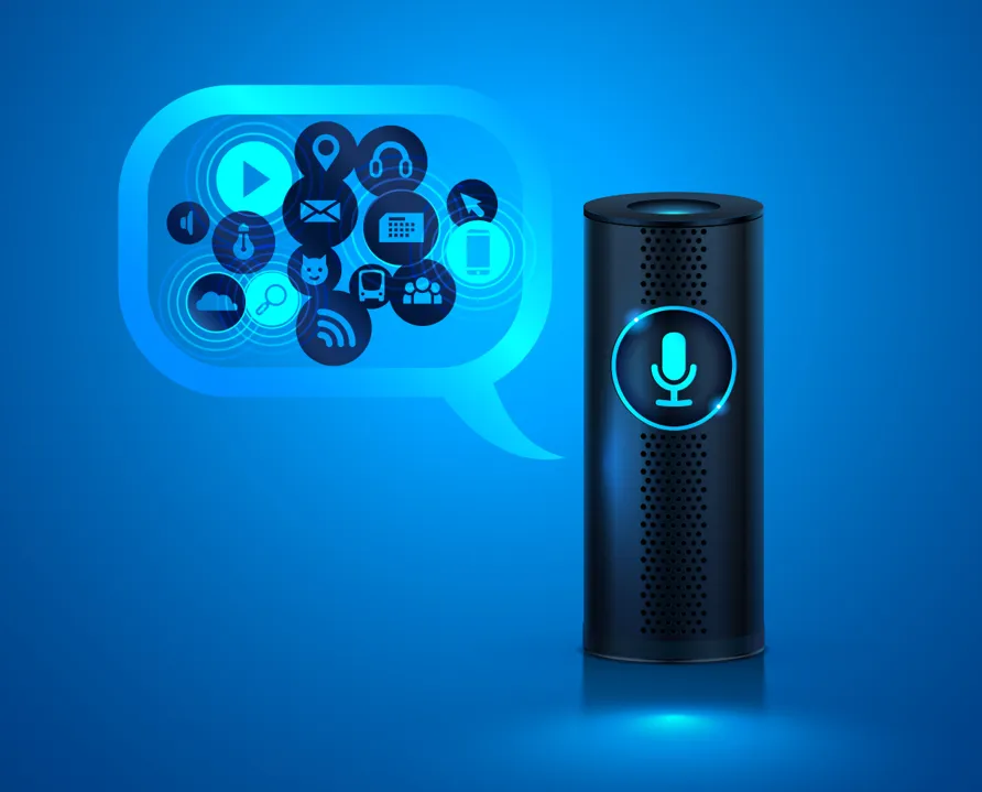
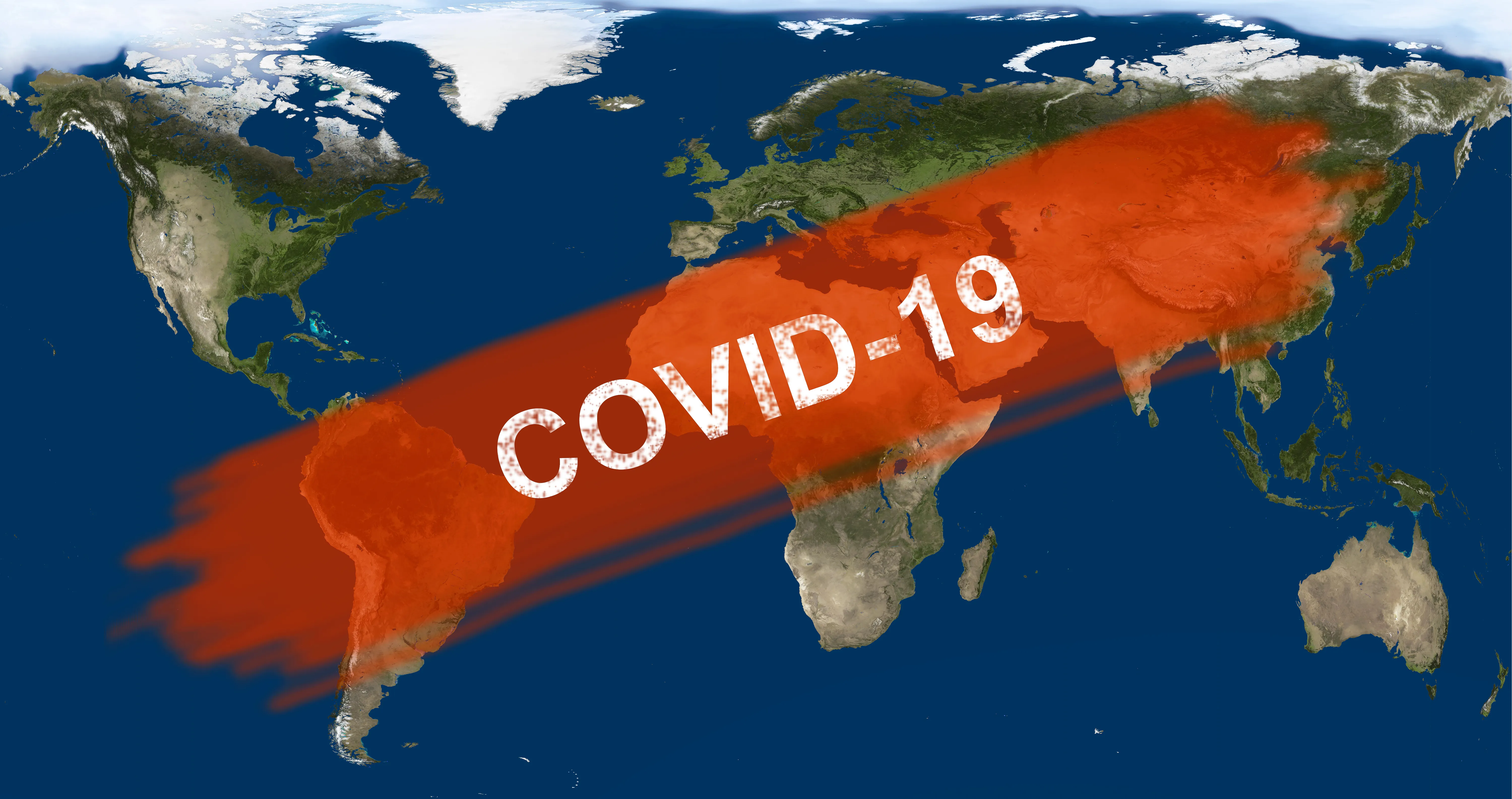
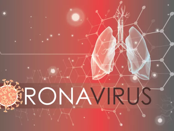
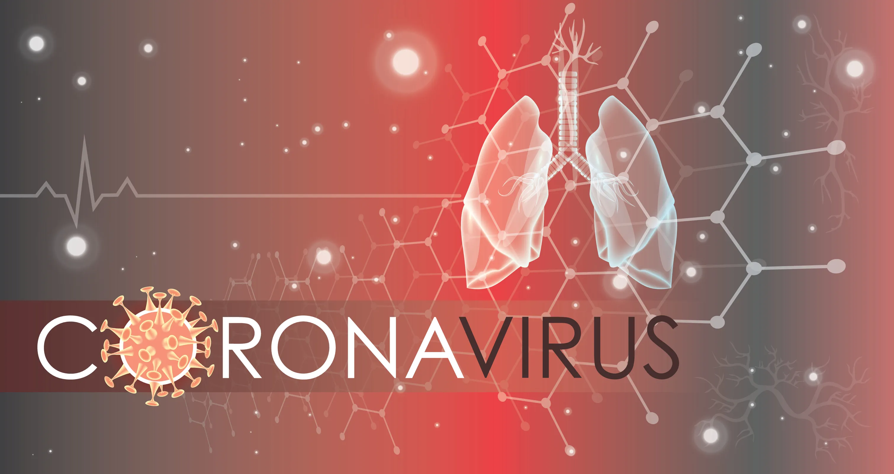
The COVID-19 pandemic (caused by SARS-CoV-2) has disrupted lives around the world more than any other catastrophic event in living memory. Those of us fortunate enough to work from home are cheering on the people who care for our health, transport our packages, work in grocery stores and pharmacies, clean public streets and buildings, and keep utilities up and running — as well as everyone else on the front lines of battling this pandemic. Working from home also gives us time to reflect and ask: How does the world return to normal and how can we help?Crises like the COVID-19 pandemic accelerate social and technology trends because the need for new solutions grows urgent. Looking at epidemiological models can reduce complex disease progression to a series of simple numbers, the most important of which is R nought (R0) value. R0 is simply how many other people a sick person infects. If each sick person infects less than one person, R0 1, the spread of disease will end. But if each sick person infects more than one other person, the disease spreads and may become a pandemic. According to the journal Emerging Infections Diseases, SARS-CoV-2 has an R0 of 5.7, making it far more infectious than the influenza pandemic of 1918.Given the severity of the current pandemic, society has taken huge efforts to reduce R0: mask-wearing, social distancing, avoiding face touching, frequent handwashing and quarantines are all ways to reduce R0.Scientists and engineers are working hard to develop new solutions and evaluate existing technologies that could have a big impact on R0. One of these is the mass deployment of touchless technologies. We’re now aware that every time we touch a surface, we potentially spread disease. I have personally started using touchless Apple Pay at retail checkouts whenever possible and even seek out and remember which stores have enabled Apple Pay. Each time I need to touch an elevator button, security keypad or walk signal button at an intersection, I contort my arms to touch them with an elbow.Since I’m in the electronics industry, I find myself considering which devices have the greatest potential for reducing the number of touchpoints in our daily lives. Motion and ultrasound sensors are definitely promising, but the mainstream adoption of the voice interface makes it the most interesting and scalable touchless technology.New voice technologies are more reliable and secure than ever. The success of cloud-based voice assistants such as Amazon Alexa, Apple Siri and Ok Google has familiarized consumers with the ease and convenience of voice, but these high-powered AI assistants generally require high power and a reliable internet connection. The next wave of voice technology will be much lower in power, fast, private and require no internet connection. This edge-powered voice interface will not play music or tell you the weather, but it will perform many other useful and simple functions, such as operating an elevator, opening a door or changing the volume on your TV. One great example of this local voice command is the Simple Human trash can that can open and close in response to your voice. Opening and closing a garbage may be simple, but a voice-activated model enhances convenience and safety with total privacy.The requirements for deploying voice technology to support more touchless applications include: Low power — to run for months or years between battery changes Robust and reliable— to last over a decade indoors or out Locally processed data — to ensure security and privacy without an internet connection Consumer adoption of touchless and voice technologies has been growing for years, but the COVID-19 crisis highlights the critical benefit of these technologies in reducing the spread of disease. Making high touchpoints voice-powered would eliminate a disease vector and reduce R0 during pandemics as well as during normal cold and flu seasons. Any technology that helps reduce R0 should be deployed as quickly as possible to give us one more way to thwart the virus that is changing life as we know it.As the only supplier of piezoelectric MEMS microphones – which are natively immune to environmental contaminants such as water, humidity, salt, dust, dirt and oil — Vesper is uniquely able to provide outdoor-hardened microphones that are durable enough to support voice-interfaces in hot, wet, dusty or dirty conditions. In fact, we’ve earned the highest waterproof rating for any MEMS microphone – IP57 – which makes me hope that one day soon I’ll use just my voice to tell a crosswalk signal that I need to cross the street.Vesper has also developed a proprietary technology called ZeroPower Listening, which makes it possible to embed always-listening voice interfaces in battery-powered devices with battery life measured in months or years. And that’s just the beginning of how we’ll use voice interfaces in high-touch applications. From voice-controlled parking kiosks and elevator buttons to the treadmill at the gym, the less we touch hard surfaces, the safer we’ll be from picking up SARS-CoV-2, influenza viruses or other pathogens as we go about our daily lives.Learn how Vesper’s low-power and rugged MEMS microphone technology can help designers create seamless voice interfaces for a wide range of indoor and outdoor applications at Smart Home, Smart Office, IoT and Automotive/Industrial.Matt Crowley is CEO of Vesper Technologies, developer of the world’s first piezoelectric MEMS microphone. With five rapid product rollouts in just five years and tens of millions of units shipping to tier one clients across the globe, Matt has grown Vesper from a research-oriented startup to a bonafide commercial business.Under his leadership, Vesper has earned an impressive collection of awards including a 2019 Best of Sensors Award, Innovation Award nods at CES 2018 and 2019, and two Annual Creativity in Electronics (ACE) Awards.Before Vesper, Matt held leadership positions at piezoelectric MEMS pioneer Sand 9, the Boston University Office of Technology Development, and Mars Co strategy consulting, where he advised Fortune 500 companies on operational and strategic issues.Matt received an interdisciplinary degree in Physics and the Philosophy of Science from Princeton University. He is proficient in Japanese, having lived in Japan.Vesper is a member of MEMS Sensors Industry Group (MSIG), a SEMI technology community, that enables the MEMS and sensor industry to address common challenges, innovate and accelerate business results.
Read More
Part 1 of 2Read Part 2. While companies navigate the ongoing COVID-19 crisis, corporate leaders should be evaluating a number of key business continuity issues as well as steps they can take to not only react to business disruptions but also reshape their business and recovery plans.We spoke with Dan Steele, Senior Director and the APAC Head of Environmental, Health, Safety, and Security (EHS S) at GLOBALFOUNDRIES (GF) Singapore, via teleconference for insights into the best practices he and his team have implemented from their Business Continuity Plan (BCP) to guide them through the health crisis.SEMI: How did GLOBALFOUNDRIES Singapore first respond when the country reported its first COVID-19 case?Steele: Since the early days of our company, we have had a Business Continuity / Crisis Management (BCCM) team in place that is responsible for business continuity planning for the site. At the beginning of this journey with the coronavirus, we believed in two truths: maintaining the safety and well-being of our employees and consistently communicating precautionary measures the company has taken to protect them and our business. These actions are critical to keeping our employees safe, while keeping the anxiety level low. By informing and updating employees in a timely manner, we ensure that they are well-educated about the crisis as it unfolds and the foreseeable circumstances that could be ahead of us. Once the world was well into the coronavirus outbreak, our CEO declared in a message to all employees that “we entered this pandemic crisis together, and we will exit it together.”We have also established links to pertinent government websites and made them conveniently available to ensure employees have access to the latest available information for their personal lives.SEMI: What actions has GF Singapore taken in response to the crisis so far?Steele: On January 29, our BCCM team activated the first line of defense by initiating temperature checks at all building entrances for every individual including employees, contractors, visitors, and customers who come into our facilities. We asked each to declare their state of health and travel history and issued a temperature card to every employee and resident contractor. They are all required to record their temperature twice daily – once before coming to work and again at midday – and they present the temperature log to security upon their arrival.The following week, our teams split into an A/B work arrangement to ensure continuity of our operations. We proactively pared down our teams to the staff essential for our on-site operations, while enabling the rest to work from home. We also advised our most vulnerable employees with impaired immune systems or who are pregnant to work from home. Concurrently, we moved all meetings of 10 or more people to virtual communications and only allowed meetings with fewer than 10 to be held in rooms with participants sitting at least one meter apart. We informed our customers of our efforts and moved all planned on-site visits to online visits.In line with Singapore’s efforts to curb the spread of COVID-19 within the community, GF restricted site access of people who had recently traveled to countries with sustained community transmission and regularly updated the restriction list. To conduct contact tracing, we created our two degrees of separation list that we used to track employees with families and close associates who were linked to a COVID-19 case. Employees provided the information voluntarily. On our campus, we enforced strict safe distancing measures by limiting access to meeting rooms, marking off-limits tables and removing chairs in the cafeteria, limiting the number of elevator riders to no more than four, and placing boxes or other spacing indicators at smoking zones, bus stops and temperature-taking lines. We also initiated a daily log of employees taking the company buses tagged to the bus number, time, and employee identification numbers in anticipation of the need for contact tracing.Most recently, when the Singapore-Malaysia border closed, we activated the next phase of our BCP that was already in place – housing over 450 Malaysian employees in Singapore hotels.Throughout this crisis, we continuously monitor and evaluate possible impacts to our supply chain to ensure the continuity of our business. This is a standard element of our ongoing business continuity management system.Most importantly, we frequently communicate with our employees and tell them everything the company is doing and why we are doing it. We encouraged employees to monitor their health, stay home if they are unwell, and seek immediate medical treatment if necessary at one of our panel clinics or other medical facilities.SEMI: What are your top concerns amidst this health crisis?Steele: At GF, we are managing through the crisis with an unwavering focus on two guiding principles: the safety and well-being of our worldwide team, their families and communities; and delivering on our commitments to our clients. As the world’s leading specialty foundry, GF has a unique role in the global supply chain. Our semiconductor technology is vital to a range of industries including health care, communications, infrastructure and security. With these priorities in mind, the company undertook unprecedented steps and has adapted to the crisis by dynamically adjusting its protocols, health and safety measures, and business processes to protect its teams while maintaining manufacturing excellence.We are committed to safeguarding the well-being of our employees while supporting and sustaining our on-site operations and protecting customers’ products. A major concern is the impact on our employees. We understand that COVID-19 can be infectious even if an individual is asymptomatic – we are always concerned that temperature screening alone is not sufficient. This is the reason that from day one we have encouraged our employees to monitor their health, follow all government advice for proper hygiene and seek medical attention if unwell as early as possible, and not come to work.Dan Steele has over 25 years of experience in environmental, health and safety, and security operations. He has also held other leadership roles in facilities engineering, quality, reliability and assurance, and risk management.Bee Bee Ng is president of SEMI Southeast Asia.
Read More
Japan’s Prime Minister Shinzo Abe declared a state of emergency for Tokyo, Osaka and five other prefectures[1] on April 7 in response to a startling increase of COVID-19 infections in the region’s cities in an uneasy moment for its domestic semiconductor industry. The declaration, effective through May 6, authorized the six prefectural governors to strengthen curbs on the spread of the virus and included guidance for citizens to stay home and restrictions on operations of non-essential businesses.With Japan supplying some 40 percent of the world’s chip production equipment and materials, the declaration stirred fears among semiconductor manufacturers that their uninterrupted operations – critical to sustaining the global industry – might be at risk. Japan Government Designates Semiconductor Industry as EssentialIn April 7 and 11 revisions to its Basic Policies for Novel Coronavirus Disease Control, the Japanese government allayed those concerns by designating semiconductor manufacturers essential businesses – a stark acknowledgment of the chipmakers’ vital role in combatting the novel coronavirus. The policy stated:“Among medical and manufacturing industries, we request the continuation of the following business operators in consideration of infection prevention: operators who are difficult to stop production line due to the characteristics of the equipment (such as blast furnaces and semiconductor factories); and operators who produce essentials (including important items in supply chains) for protection of the people who need medical care and support, as well as for maintenance of social infrastructure. We also request the continuation of the business operators who sustain medical care, the lives of the people, and maintenance of the national economy.”[2]SEMI Japan Reaches Out to Prefectures to Urge Essential Business Designation Equipment and materials shortages can halt production of an entire fab line and ripple through intricately connected global supply chains to stifle the production of end devices including the electronics critical to COVID-19 treatments. Electronic devices also play a central role in containing the virus’s spread by enabling artificial intelligence (AI), data analytics, digital communications, telemedicine, robotics, remote health monitoring, telecommuting, online shopping and other digital services.The essential business designation was explicit recognition that Japan’s semiconductor supply chain is integral to the global chip production ecosystem and worthy of the same protections the government has implemented for semiconductor companies. With SEMI members operating in Japan’s 47 prefectures, I sent letters to all prefectural governors three days after the second policy revision, urging them to apply the same designation, and the SEMI Japan team is following up to secure their support.SEMI Japan Encourages Government to Exempt Members from Travel Restrictions The Japan Foreign Ministry on March 31 raised to level 3 its travel advisory for 49 regions including the U.S., China, Taiwan and South Korea, encouraging Japanese citizens to avoid travel regardless of purpose to blunt the international spread of the coronavirus. SEMI Japan is working with the Semiconductor Equipment Association of Japan to urge the government to exempt semiconductor supply chain companies from the level 3 travel restrictions if they implement measures to prevent domestic infections and contagion in the visited regions. The exemptions would allow supply chain companies to install and service equipment at fabs – one key to maintaining smooth, uninterrupted operations.SEMI Supports Members with COVID-19 ResourcesSEMI international headquarters and regional offices are here to help you, our members. For more information on our webinars, surveys, best practices and other information designed to help you meet the challenges of the pandemic, please visit the SEMI Coronavirus Updates Resources page.[1] The six prefectures are Tokyo, Kanagawa, Chiba, Saitama, Osaka, Hyogo and Fukuoka.[2] Provisional translation by Ministry of Health, Labour and Welfare. Full document is available at https://www.mhlw.go.jp/content/10900000/000620733.pdf.Jim Hamajima is president of SEMI Japan.
Read More
The seemingly simple act of commanding consumer devices by voice is a choice that nearly 118 million Americans now make every day, according to a recent report from eMarketer, the digital marketing research firm.While the voice interface is convenient for users, its implementation comes at the potential loss of individual privacy. The reason? Always-on, always-connected voice-first devices such as Amazon Alexa and Google Home require a wall plug and an internet connection to powerful cloud processors, making it possible for cloud companies — however benignly — to collect data on personal habits, location and conversation that were never intended for sharing. Move processing to the edgeTo address concerns over user privacy, device designers are attempting to do more of the audio processing within the consumer device, rather than sending users’ voices into the cloud. Moving more processing to the edge is a trend across the Internet of Things (IoT) industry, and not just for voice data but for other types of sensitive or proprietary data as well.Yet designers have realized limited success because the conventional approach to always-listening edge processing is notoriously inefficient: It digitizes and processes 100% of incoming sound data even though up to 90% of the data is irrelevant noise. This digitize-first approach wastes vast amounts of system power digitizing and analyzing the audio signal as it searches for a wake word when there isn’t even speech present, making it impractical for use in small, battery-operated devices.Workarounds don’t workTackling this power issue is critical to keeping private data secure. Unfortunately, it’s also exceptionally difficult. Design engineers have tried workarounds to decrease power consumption in an always-listening system, including duty cycling and reducing the power of each individual component in the audio signal chain that handles the data. The reality is that these kinds of approaches don’t address the root cause of the problem: too much data.To truly tackle the problem, we need to change our approach to a system solution, not a component solution. By moving to a more efficient edge architecture that intelligently minimizes the amount of data that moves through the system, we can focus the system’s energy resources on analyzing voice and not on searching for a wake word in irrelevant noise. Analyze, THEN digitize It’s time to move away from the digitize-first approach that has dominated voice wake-up device architecture since the invention of voice-first applications.Inspired by the way the human brain efficiently filters incoming information, differentiating, for example, a dog bark from a baby’s cry, an ultra-low-power analog machine learning technology is changing this paradigm. For the first time, device designers can use low-power analog machine learning to detect which data are important for further processing and analysis prior to data digitization.Leveraging an analyze-first architecture, a new analog neuromorphic semiconductor platform allows the higher-power-processing components in the system to stay asleep until voice has actually been detected, and only then does it wake them to listen for a possible wake word.Delivering a post-microphone audio chain that draws as little as 25µA of current when always-listening and collecting preroll data, this analyze-first architecture allows designers to extend battery lifetime significantly. That’s the difference between smart earbuds that run for weeks instead of hours or a battery-powered smart speaker that runs for months instead of weeks.More importantly, it’s the difference between the current always-listening devices that indiscriminately record and send all sound data to the cloud, and one that has the localized intelligence to select and send only the relevant data, reducing the user’s vulnerability to the loss of private data.Balance convenience with privacyThe trade-off between making our lives easier and keeping our personal information private is a choice that we are asked to make throughout our day in a hundred different ways. Bringing more audio processing capability to the mobile device without draining the battery is the first step toward delivering more secure voice-first solutions. But to succeed in this effort, we must shift to a bio-inspired architecture that determines which data are important and requires further processing at the earliest point in the signal chain. Once we move to the analyze-first approach, only a small fraction of the tens of zettabytes of data collected by the forthcoming generation of always-on IoT devices will require further processing in the device and in the cloud.A better balance between cloud and edge processing is a better balance between convenience and privacy, and that’s a win for everyone.About the AuthorTom Doyle is CEO and founder of Aspinity. He brings over 30 years of experience in operational excellence and executive leadership in analog and mixed-signal semiconductor technology to Aspinity. Prior to Aspinity, Tom was group director of Cadence Design Systems’ analog and mixed-signal IC business unit, where he managed the deployment of the company’s technology to the world’s foremost semiconductor companies. Previously, Tom was founder and president of the analog/mixed-signal software firm, Paragon IC solutions, where he was responsible for all operational facets of the company including sales and marketing, global partners/distributors, and engineering teams in the US and Asia. Tom holds a B.S. in Electrical Engineering from West Virginia University and an MBA from California State University, Long Beach. For more information, please visit https://www.aspinity.com/Technology.Aspinity is a member of MEMS Sensors Industry Group (MSIG), a SEMI technology community, that enables the MEMS and sensor industry to address common challenges, innovate and accelerate business results.
Read More
Ischemic stroke is the leading cause of long-term disability worldwide, affecting over 13 million people each year and costing tens of billions of dollars. Sensome, a French medtech that offers connected medical devices, has developed micrometric AI-powered impedance sensors that can identify the biological nature of the tissue they touch in real-time. Integration of this proprietary technology into a probe to guide medical devices in arteries (a guidewire) has given rise to Sensome’s first product, Clotild®, which recognizes blood clot types in ischemic strokes so clots can be treated faster to improve patients’ chances of a full recovery. The Sensome technology also helps transform the current standard of care in oncology.SEMI spoke with Franz Bozsak, CEO and co-founder of Sensome, about innovative medical technology trends and how microelectronics plays a crucial role.SEMI: When did your adventure with Sensome start? Bozsak: My former Ph.D. advisor Abdul Barakat and I spun-out Sensome from the Ecole Polytechnique in Paris in early 2014 after receiving a 200.000 Euro grant from the French government. We then developed a micrometric impedance sensor that coupled to machine-learning algorithms to identify biological tissues on contact. We are still integrating this sensing technology with existing medical devices in order to create a new category of smart medical devices that provides physicians with relevant insights during their interventions and treatments. These additional insights aim to render healthcare treatments more effective by reducing the risk of complications and the cost of interventions while improving patient monitoring.SEMI: How are strokes typically treated? Bozsak: Before 2014 the almost exclusive way of treating ischemic stroke was by injecting tissue plasminogen activator (tPA) intravenously in order to chemically dissolve an arterial clot. This treatment approach has severe limitations and can only be used in the first 4.5 hours following the onset of a stroke. In 2015, several randomized clinical trials demonstrated the efficacy of a new treatment modality: mechanical thrombectomy.Medical devices that allow a clot to be removed mechanically either using a grid-like structure (a stentriever) or by aspirating the clot using an aspiration catheter completely changed the paradigm in the treatment of ischemic stroke for up to a third of all patients. This new intervention removes the clot in up to 90% of all cases and can for certain patients be used up to 24 hours after the onset of the stroke.Mechanical thrombectomy is now one of the most effective medical treatments in the world. The clinical data gathered over the past years also shows that, in order to maximize the patient’s chances to lead a life free from disability after a stroke, it is not only a question of getting the clot out but also about how the clot was removed. Removing the clot on the first attempt significantly increases the patient’s chances of recovery – the first-pass-effect that is now the objective when treating ischemic stroke patients. And this is exactly where Sensome wants to help since clot removal after several attempts increases risk for patients. SEMI: How did you improve mechanical stroke treatments?We have integrated our sensor technology into a guidewire, the first device to enter a patient’s blood vessels for navigation to the clot. Once in place, the smart guidewire – called Clotild® – guides the thrombectomy device to provide the physician with information on the clot to help the physician choose the thrombectomy device with the highest chances of achieving the first-pass-effect. SEMI: Medical technology has made astonishing advances over the years. How did Sensome develop the micrometric AI-powered impedance sensors?Bozsak: The development of a product like Clotild® would have not been possible five years ago, and many people considered what we wanted to achieve simply incredible. Today, we can answer those same people: We knew it was almost impossible and therefore we just did it. By combining diverse semiconductor technologies, we were able to build the smallest impedance meter in the world. This was then integrated into a guidewire that can be connected via a transmitter to a tablet that serves as the interface with the physician. The guidewire provides impedance measurements that can be analyzed by a machine-learning algorithm, which in turn identifies the tissue in contact with the sensor. A very diverse team of people, collaboration and several different disciplines such as micro-electronics, data science, biology and engineering were required to make this happen.Our ambitious team has been able to flourish and accomplish their ideas in the very stimulating and resourceful environment of the Ecole Polytechnique, while being embedded into the rich and fertile start-up ecosystem of Paris. It is the combination of all these factors taken together that have made our innovation possible.SEMI: What are the main challenges and what are the market opportunities? Bozsak: Bringing semiconductor technology into the medical field is not a straightforward process. The primary hurdle is the simple fact that medical device production volumes are not comparable with consumer electronics volumes and that development cycles are much longer due to regulatory constraints. Both factors are, at first sight, not necessarily compatible with today’s business model of the semiconductor industry. At the same time, this is also a unique opportunity for the semiconductor industry to diversify and expand into a new field – sensors and, in particular, their seamless integration into the healthcare workflow, are a key driver for the healthcare sector of the future. And to achieve this objective, semiconductor technologies are key. What is beneficial, in my opinion, is that the quality standards and requirements of the semiconductor industry are highly compatible with the needs of the medical device industry.SEMI: Are market fragmentation and the high level of regulation making medtech innovation harder?Bozsak: Both are challenging but very rewarding to pursue since the impact on a patient’s life can be profound. Innovation is harder because many stakeholders are involved in ensuring the success of a medical device launch. The involved, milestone-driven, highly regulated process of developing a medical device and bringing the device to the market assures its eventual success. The development process differs very much from those for normal consumer devices. In our case the beneficiary, the patient, is not necessarily the user of the device but rather the physician. The physician is not necessarily the buyer of the device, but the hospital. The hospital is not necessarily paying the device, but ideally the government.The interests of all these stakeholders need to be satisfied to bring a successful device to the market.SEMI: What are your expectations regarding the future of medtech digital innovation? Bozsak: This is the right moment for the medical device and semiconductor industries to come together. The healthcare sector is not low on medical needs for which innovative ideas exist, and the semiconductor industry has many technologies that can enable these ideas to generate solutions. But to make this happen, both sectors need to collaborate. Working together requires both sides to understand their respective needs and constraints. The earlier the knowledge exchange starts, the more powerful the solutions. SEMI MedTech Forum at SEMICON Europa last year was a wonderful opportunity for Sensome to get this discussion going. We are looking forward to continuing the exchange and push the frontiers of the possible further to create the future of digital healthcare.Franz Bozsak, CEO and co-founder at Sensome, obtained a M.S. in Aerospace Engineering from the University of Stuttgart and a Ph.D. from the Ecole Polytechnique in Biomedical Engineering on the optimization of stents. He is a graduate of the Stanford Ignite/Polytechnique business program. In 2014, he co-founded Sensome and has since built a team of renowned scientists, engineers and doctors to realize his vision of connected medical devices. He was named Innovator Under 35 by the MIT Technology Review in 2016. Serena Brischetto is a marketing and communications manager at SEMI Europe.
Read More
SEMI has urged government representatives around the U.S. and world to designate the semiconductor industry as an essential business so operations at companies across the chip supply chain can continue without interruption as the spread of COVID-19 continues. SEMI President and CEO Ajit Manocha assured the U.S. and global officials that SEMI members – the device makers and suppliers of chemicals, materials, components, design tools and equipment at the heart of chip manufacturing – “are employing all measures necessary to maintain the health and safety of their employees and local communities” to help contain the virus. Manocha last week sent letters to the governors of 16 states and the chairs of the National Governors Association, U.S. Conference of Mayors, National League of Cities, and National Association of Counties requesting consideration of the semiconductor industry as an essential business if shelter-in-place or similar orders are issued to curb the spread of COVID-19. More than half of U.S. states have imposed shelter-in-place or stay-at-home orders in the past month. The designation would allow SEMI members to maintain continuous operations to ensure that manufacturing of components for critical infrastructure equipment, the defense industrial base, and other vital technological products and services is not jeopardized. Semiconductors are the foundation of modern electronics and information technology and are critical in helping health workers effectively treat COVID-19 symptoms, Manocha told the officials. The devices also play a central role in containing its spread by enabling artificial intelligence (AI), data analytics, digital communications, telemedicine, robotics, remote health monitoring, telecommuting, online shopping and other digital services.Manocha urged state and local officials to follow guidelines issued on March 19 by the Department of Homeland Security (DHS) Cybersecurity Infrastructure Security Agency (CISA) identifying “manufacturers and supply chain vendors that provide hardware and software, and information technology equipment (to include microelectronics and semiconductors) for critical infrastructure as ‘essential critical infrastructure workers.’” Most states issuing shelter-in-place or stay-at-home orders have followed the DHS guidelines and/or separately designated the semiconductor industry an essential business. Likewise, other nations have recognized the power of technology in effectively containing COVID-19 and similarly designated the semiconductor industry an essential business.On March 27, SEMI, the Semiconductor Industry Associations in China, Europe, Japan, Korea, Singapore, Taiwan and the U.S., as well as several other trade associations in Asia issued a statement “calling on all governments to specify semiconductor industry operations as ‘essential infrastructure’ and/or ‘essential business’ to allow continuity in operations.” The global semiconductor supply chain forms a highly intricate network consisting of research, design and manufacturing operations. Operating restrictions in one region can compromise production in others, leading to inefficiencies and breakdowns that cascade across the supply chain.With semiconductors underpinning vital sectors of the global economy, the chip associations called on all global governments at all levels – central, states, provinces and localities – to help protect the uninterrupted operations of domestic semiconductor companies and their suppliers by applying the essential infrastructure or essential business designation.Joe Pasetti is Vice President of Global Public Policy and Advocacy at SEMI.
Read More
Skills are the key to the future. It is thanks to its skilled workforce that Europe will reap the benefits of the green and digital transitions and remain competitive. At the same time, upskilling and reskilling is a clear social policy because it ensures that workers can more easily navigate from one job to another.Microelectronics is at the crossroads of many sectors, such as the automotive industry, manufacturing, health, and energy. The European electronics industry is facing an acute shortage of skills in all tiers of its value chain, particularly in electronics design, both digital and analog, and in system and software engineering. A sustainable provision of qualified personnel is key to maintain competitiveness and innovation leadership. Yet, companies in this area suffer from a critical shortage of engineers with competence in microelectronics technology and design. The rapid evolution of the electronics industry calls for a continuous update of skills and knowhow.Vocational education and training has an important role to master these challenges. Modern, inclusive and dynamic vocational education and training programmes are a pre-requisite to remain competitive in the digital age. We must support agile partnerships to develop skills for smart industrial specialisation and the green and digital transitions. Everybody must be on board to shape the workforce transformation in Europe: industry, social partners, education and training organisations, as well as policymakers. The Blueprint for sectoral cooperation on skills launched in 2016 is an excellent model for strategic collaboration and will be extended.The Commission has recently proposed an update of our successful Skills Agenda for Europe. One key element is the new Pact for Skills, in order for all stakeholders to generate new concrete commitments to invest in upskilling and reskilling. It will help us to respond to the extent and speed of change in the economy and society. I warmly invite the microelectronics industry to participate in the Pact.I welcome the fact that SEMI and its 19 partners from 14 countries launched METIS – MicroElectronics Training, Industry and Skills Erasmus+ Project – in November 2019. METIS will receive 4 million EUR EU funding to implement a comprehensive strategy with a view to identify and fill skills shortages, to tackle skills mismatches, and to support upskilling and reskilling in order to address the challenges of the future of work and digitalisation.Nicolas Schmit is European Commissioner Jobs and Social Rights.
Read More
In the future, electronics-related gear including advanced driver-assistance systems (ADAS) will account for a whopping 50 percent of automotive costs. More importantly, with more control of vehicles shifting to automation, the margin of error in component performance and reliability will become vanishingly small as zero defects become the new safety standard.SEMI spoke with Antoine Amade, Senior Regional Director EMEA, Entegris about zero defects as a new collaborative approach necessary to shape the car of the future and the automotive industry.SEMI: The next generation of automobiles will be more electric, autonomous and connected. What is the most pressing next step for automotive players to pursue this goal? Amade: The automotive ecosystem faces many challenges. For example, when cars become autonomous, their interaction with the cloud and the massive amount of data computed simultaneously could be vulnerable to cyberattacks capable of seizing control of the vehicle.Another example is the use of artificial intelligence (AI) as there is a big opportunity to explore and define the right architecture while also meeting automotive quality requirements. The quality challenge will be amplified by advanced nodes. Reliability is also critical since 90 percent of device failures are extrinsic, or unrelated to device design. Today, the top priority should be to eliminate latent defects, those that remain undetected until the product is in use. These latent defects may appear at some future point in the life of vehicle – 1 month, 1 year, 10 years, etc. This is the vital focus of the carmaker and the supply chain.SEMI: With in-line metrology tools reaching their detection limits, how will the industry reduce latent defects? Amade: Minimizing latent defects is now a top priority in semiconductor fabs. However, there is a gap between visible and non-visible defects. Although fabs can detect small defects, human intervention is still needed to manage them. We are witnessing a fundamental shift in the contamination control strategy in auto chip production, from contamination control for yield to contamination control for reliability. The shift is born of the recognition that all particles, regardless of size, and parts per trillion (ppt) concentration levels of contaminants matter, impact both defectivity and reliability. Contamination management will play a key role in enabling the industry to reach parts per billion (ppb) failure rates at the component level. SEMI: How will the industry reach the goal of zero defects? Amade: A sound contamination management strategy that follows three main axes of actions will be one key to reaching zero defects: the ambient air in the fab, the wafer’s environment over its lifetime, and the integrity of the materials in the clean chemical delivery pathway.Contamination management in each of these three areas presents opportunities to limit process variability. The first step in limiting variation is detecting it, which can be difficult when the contaminants causing the variation are hard to identify or caused by an unexpected event. When a contaminant signature can be detected, it leaves clues to its root cause. Careful scrutiny of these signatures can inform a contamination control strategy to eliminate the root cause and reduce overall defectivity.SEMI: What collaborative engagement model do you see as the best for reaching zero defects? Amade: Entegris sees the SEMI Global Advisory Automotive Council (GAAC) as the perfect collaboration platform for the entire automotive semiconductor ecosystem, from car manufacturers to material suppliers. Entegris is also a member of the Platform for Automotive Semiconductor Requirement Across the Supply Chain (PASRASC). Both forums help raise the visibility of key challenges and potential solutions.Collaboration starts with agreement on a definition of automotive based on existing standards and guidelines that must be communicated across the value chain. Another important element for collaboration is standardizing on how new materials such as SiC Semiconductors (silicon carbide) should be used. Entegris plays a leading role in contamination management for defectivity reduction through its New Collaborative Approach (NCA) platform, which brings a new level of knowledge sharing to all those involved in detecting and improving defectivity.SEMI: Can you explain the New Collaborative Approach in more detail?Amade: During the SEMI Smart Transportation Forum at SEMICON Europa, we presented the process and tools we have been developing in collaboration with car makers and are implementing with chipmakers as part of our New Collaborative Approach. Our data-driven tools compare current contamination solutions practices and identify optimization opportunities. A good indicator of the maturity of the ecosystem, the tools allow chipmakers to compare the contamination mitigation practices of peers with their own and identify hot topics for advancing contamination management strategies. Every year, during Entegris Technology Days, we share best known methods, case studies, and review fab processes in order to propose customized solutions. It is all about improving defectivity.Mr. Amade joined Entegris in 1995 as an Application Engineer in its semiconductor business. In his current role as EMEA/NA Sr. Director, Mr. Amade is focused primary on growing the semiconductor business in Europe and Middle East through market strategies, and the management of sales, customer service, and marketing teams. Mr. Amade held leadership positions at Entegris in functions including gas microcontamination market management, strategic account management, and regional sales management. Mr. Amade has a degree in Chemical Engineering from ENS Chimie Lille and is a member of the SEMI Electronic Materials Group and the Global Automotive Advisory Council for Europe (GAAC).Serena Brischetto is a marketing and communications manager at SEMI Europe.
Read More